Topological Materials in Spintronics: Dirac and Weyl Semimetals for Next-Gen Devices
AUG 27, 20259 MIN READ
Generate Your Research Report Instantly with AI Agent
Patsnap Eureka helps you evaluate technical feasibility & market potential.
Topological Materials Evolution and Research Objectives
Topological materials represent a revolutionary frontier in condensed matter physics, emerging from the convergence of quantum mechanics and topology. Since the theoretical prediction and experimental confirmation of topological insulators in the mid-2000s, this field has expanded dramatically to include a diverse family of materials with unique electronic properties. The discovery of Dirac and Weyl semimetals in the 2010s marked a significant milestone, introducing materials with electronic structures that host relativistic quasiparticles and topologically protected surface states.
The evolution of topological materials research has progressed through several distinct phases. Initially focused on two-dimensional quantum Hall systems, the field expanded to three-dimensional topological insulators characterized by insulating bulks and conducting surfaces. The subsequent identification of topological semimetals—including Dirac, Weyl, and nodal-line semimetals—has further enriched the landscape, offering platforms with extraordinary electronic transport properties and spin-momentum locking phenomena.
Recent advances in material synthesis techniques, particularly molecular beam epitaxy and chemical vapor deposition, have enabled the fabrication of high-quality topological materials with precisely controlled structures. Concurrently, characterization methods such as angle-resolved photoemission spectroscopy (ARPES) and scanning tunneling microscopy have become increasingly sophisticated, allowing for detailed examination of the electronic and spintronic properties of these materials.
In the context of spintronics, topological materials offer unprecedented opportunities due to their intrinsic spin-orbit coupling and topologically protected states. These properties manifest as spin-polarized currents and extraordinary magnetoresistance effects that persist even in the presence of impurities or structural defects. The robustness of these phenomena makes topological materials particularly promising for next-generation spintronic devices that require high efficiency and stability.
The primary research objectives in this field now center on several key areas. First, expanding the library of synthesizable topological materials with properties optimized for specific applications. Second, developing reliable methods to control and manipulate the topological states, particularly through external fields or proximity effects. Third, engineering practical device architectures that effectively harness the unique properties of these materials for information processing and storage.
Looking forward, the integration of topological materials with conventional semiconductor technologies represents a critical challenge and opportunity. The ultimate goal is to develop hybrid systems that combine the advantages of topological protection with the established infrastructure of semiconductor electronics, potentially enabling quantum computing architectures, ultra-low power logic devices, and novel memory technologies with unprecedented performance characteristics.
Market Applications for Spintronics-Based Devices
Spintronics-based devices leveraging topological materials are poised to revolutionize multiple market sectors due to their unique capabilities in manipulating electron spin rather than charge. The data storage industry represents the most immediate commercial opportunity, with magnetic random-access memory (MRAM) already entering production phases. These non-volatile memory solutions offer significant advantages in power consumption, reducing energy usage by up to 70% compared to conventional memory technologies while providing faster access times and unlimited write endurance.
The computing sector stands to benefit substantially from spintronics implementations in logic devices. Topological materials enable the development of spin-based logic gates that could overcome the power density limitations of CMOS technology. Market analysts project that by 2030, spin-based computing could capture 15% of the specialized computing hardware market, particularly in edge computing applications where power efficiency is paramount.
Quantum computing represents another high-potential application area. Topological qubits based on Majorana fermions in topological materials offer inherent protection against decoherence, addressing one of the fundamental challenges in quantum computing. While still in early research stages, the quantum computing market is expanding rapidly and could represent a significant opportunity for spintronics technologies within the next decade.
Sensors and detectors incorporating topological materials demonstrate exceptional sensitivity to magnetic fields, enabling applications in healthcare for advanced medical imaging systems. The biomedical sensing market is particularly promising, with projected growth rates exceeding 20% annually for next-generation diagnostic tools.
Telecommunications infrastructure could be transformed through spintronics-based signal processing components that operate at higher frequencies with lower power requirements. The deployment of 6G networks beginning in the late 2020s will create substantial demand for such advanced components, with an estimated market value exceeding $50 billion by 2035.
Automotive and aerospace sectors present growing opportunities for spintronics applications in navigation systems, where topological material-based sensors offer superior performance in harsh environments. The increasing autonomy of vehicles and aircraft will drive demand for more robust and precise sensing technologies.
Military and defense applications constitute a specialized but lucrative market segment, with particular interest in radiation-hardened computing systems and ultra-sensitive magnetic anomaly detection. Government funding in this sector continues to grow steadily, providing a stable market for advanced spintronics technologies.
Current Challenges in Topological Semimetals Research
Despite significant advancements in topological semimetals research, several critical challenges continue to impede their practical implementation in spintronics applications. The primary obstacle remains the reliable and scalable synthesis of high-quality topological materials with consistent properties. Current growth techniques, including molecular beam epitaxy and chemical vapor deposition, struggle to produce large-area, defect-free samples with well-controlled stoichiometry, severely limiting industrial viability.
Material characterization presents another significant hurdle. The complex electronic structures of Dirac and Weyl semimetals require sophisticated analytical techniques such as angle-resolved photoemission spectroscopy (ARPES) and scanning tunneling microscopy (STM) to verify their topological properties. These methods are time-intensive and often require specialized facilities, complicating rapid material development and quality control processes.
Interface engineering between topological semimetals and conventional materials poses substantial difficulties. The preservation of topological surface states at these interfaces is crucial for device functionality, yet these states are highly susceptible to degradation from oxidation, contamination, and lattice mismatch. This sensitivity significantly complicates device fabrication and integration with existing semiconductor technologies.
Temperature stability represents another major challenge. Many topological phenomena are only observable at extremely low temperatures, typically below 100K. Developing materials that maintain their topological properties at room temperature remains an elusive goal, though recent discoveries in MnBi2Te4 and similar compounds show promise for higher-temperature applications.
The translation of fundamental topological properties into practical device metrics faces substantial barriers. While theoretical predictions suggest exceptional performance advantages, experimental devices frequently underperform due to non-ideal material quality, interface issues, and design limitations. The gap between theoretical potential and experimental reality continues to widen as more complex topological phenomena are discovered.
Computational modeling presents additional challenges. Accurate simulation of topological materials requires advanced density functional theory approaches with spin-orbit coupling considerations, demanding substantial computational resources. The predictive power of these models remains limited by approximations necessary to make calculations tractable.
Finally, standardization issues plague the field. Inconsistent fabrication protocols, characterization methodologies, and performance metrics make cross-comparison between research groups difficult, hampering collaborative progress and technology transfer to industry. Establishing universally accepted benchmarks and testing protocols represents a critical need for advancing the field toward practical applications.
Existing Implementations of Dirac and Weyl Semimetals
01 Synthesis and fabrication methods of topological materials
Various methods for synthesizing and fabricating Dirac and Weyl semimetals are described, including molecular beam epitaxy, chemical vapor deposition, and other growth techniques. These methods enable the production of high-quality topological materials with controlled properties. The fabrication processes often involve precise control of growth parameters to achieve the desired electronic band structure and topological properties.- Synthesis and fabrication methods of topological materials: Various methods for synthesizing and fabricating Dirac and Weyl semimetals are described, including molecular beam epitaxy, chemical vapor deposition, and other advanced growth techniques. These methods enable the production of high-quality topological materials with controlled properties, such as crystal orientation, thickness, and composition. The fabrication processes often involve precise control of growth parameters to achieve the desired topological properties in these materials.
- Electronic and transport properties of Dirac and Weyl semimetals: Dirac and Weyl semimetals exhibit unique electronic and transport properties due to their topological band structure. These materials feature linear energy-momentum dispersion relations, high carrier mobility, and unusual magnetoresistance effects. The electronic properties include chiral anomaly, negative magnetoresistance, and quantum oscillations. Understanding these properties is crucial for developing applications in electronics, spintronics, and quantum computing.
- Device applications of topological materials: Topological materials, particularly Dirac and Weyl semimetals, are being integrated into various electronic and optoelectronic devices. These applications include field-effect transistors, spintronic devices, sensors, and quantum computing components. The unique properties of these materials, such as high carrier mobility and topologically protected surface states, make them promising candidates for next-generation electronic devices with improved performance and novel functionalities.
- Optical and magnetic properties of topological semimetals: Dirac and Weyl semimetals exhibit distinctive optical and magnetic properties that arise from their unique band structures. These materials show unusual responses to electromagnetic radiation, including high optical conductivity, nonlinear optical effects, and circular dichroism. Their magnetic properties include anomalous Hall effect, topological Hall effect, and unique responses to external magnetic fields. These properties can be tuned by controlling the material composition and structure.
- Theoretical modeling and computational studies of topological materials: Theoretical and computational approaches are essential for understanding and predicting the properties of Dirac and Weyl semimetals. These studies involve density functional theory calculations, tight-binding models, and first-principles calculations to predict band structures, topological invariants, and surface states. Computational methods help identify new candidate materials with topological properties and guide experimental efforts in synthesizing and characterizing these materials.
02 Electronic and transport properties of Dirac and Weyl semimetals
Dirac and Weyl semimetals exhibit unique electronic and transport properties due to their topological band structure. These materials feature linear band crossings at discrete points in momentum space, leading to massless fermion-like excitations. The electronic properties include high carrier mobility, large magnetoresistance, and chiral anomaly effects. These characteristics make them promising for various electronic applications and fundamental physics studies.Expand Specific Solutions03 Device applications of topological materials
Topological materials, particularly Dirac and Weyl semimetals, can be integrated into various electronic and spintronic devices. Applications include high-frequency electronics, quantum computing components, sensors, and energy conversion devices. The unique topological properties of these materials enable novel functionalities that are not achievable with conventional semiconductors, such as dissipationless transport channels and robust quantum states.Expand Specific Solutions04 Material compositions and structures for topological phases
Various material compositions and crystal structures can host topological phases such as Dirac and Weyl semimetals. These include transition metal dichalcogenides, bismuth-based compounds, and certain oxides. The specific atomic arrangements and symmetries in these materials determine their topological properties. Engineering the composition and structure allows for tuning the position of Dirac or Weyl points in the Brillouin zone and their associated properties.Expand Specific Solutions05 Characterization and measurement techniques for topological states
Specialized techniques are employed to characterize and measure the topological states in Dirac and Weyl semimetals. These include angle-resolved photoemission spectroscopy (ARPES), scanning tunneling microscopy, magnetotransport measurements, and optical spectroscopy. These methods allow researchers to directly observe the unique band structures, surface states, and quantum oscillations that are signatures of topological materials, providing crucial information for both fundamental understanding and practical applications.Expand Specific Solutions
Leading Research Groups and Industry Stakeholders
Topological materials in spintronics, particularly Dirac and Weyl semimetals, are emerging as a transformative technology for next-generation devices, currently in the early growth phase of development. The global spintronics market is projected to reach $12.8 billion by 2027, with topological materials representing a rapidly expanding segment. Research institutions like Peking University, Tsinghua University, and MIT are leading fundamental discoveries, while companies including IBM, Intel, and KIOXIA are advancing practical applications. The technology is transitioning from laboratory research to early commercialization, with significant breakthroughs in quantum computing, data storage, and low-power electronics. Industry-academia collaborations between entities like Nanyang Technological University and corporate partners are accelerating development toward market-ready solutions.
Peking University
Technical Solution: Peking University has developed cutting-edge research on topological materials for spintronics applications, with a strategic focus on Dirac and Weyl semimetals that exhibit exceptional electronic transport properties. Their approach combines theoretical modeling with advanced material synthesis and device fabrication to create next-generation spintronic components. PKU researchers have pioneered novel synthesis methods for creating high-quality topological semimetal thin films with precisely controlled thickness and interface properties, critical for maintaining the desired topological states[12]. Their technology leverages the unique spin-momentum locking in topological surface states to achieve highly efficient spin-charge conversion, with demonstrated conversion efficiencies up to 30% higher than conventional materials[13]. A distinctive aspect of PKU's research is their development of strain-engineered topological materials, where mechanical strain is used to tune the electronic band structure and enhance desired properties for specific applications. They have successfully demonstrated functional magnetic memory prototypes using Weyl semimetal/ferromagnet heterostructures that operate with switching currents reduced by up to 65% compared to conventional spin-transfer torque devices[14]. Their recent work also explores the integration of topological materials with ferroelectric substrates to create multifunctional devices with electrically controllable magnetic properties.
Strengths: PKU's approach offers excellent energy efficiency and potentially lower manufacturing costs through their innovative synthesis methods. Their devices show remarkable resilience to external perturbations and temperature fluctuations. Weaknesses: The technology currently faces challenges with interface quality control at scale and requires further optimization for long-term stability. Some of their most promising material systems have complex compositions that may present uniformity challenges in mass production.
International Business Machines Corp.
Technical Solution: IBM has developed advanced spintronics technologies leveraging topological materials, particularly focusing on Dirac and Weyl semimetals for next-generation computing devices. Their approach combines magnetic tunnel junctions with topological insulators to achieve highly efficient spin-orbit torque switching. IBM's research demonstrates that topological materials can provide nearly dissipationless spin and charge transport channels with high spin-orbit coupling, enabling magnetic switching with significantly lower energy consumption than conventional materials[1]. Their proprietary design incorporates thin films of topological materials interfaced with ferromagnetic layers to create devices with switching currents reduced by up to 75% compared to traditional MRAM technologies[2]. IBM has also pioneered the integration of Weyl semimetals into logic devices, utilizing the unique chirality-dependent transport properties to create novel computing architectures that could potentially overcome the limitations of CMOS technology[3].
Strengths: IBM's extensive fabrication infrastructure allows for precise material deposition and device integration at industrial scale. Their approach shows superior energy efficiency and switching speed compared to conventional spintronic devices. Weaknesses: The technology requires ultra-high material purity and precise interface engineering, making manufacturing challenging. Operating temperatures are currently limited, requiring additional cooling systems for practical applications.
Breakthrough Patents in Topological Spintronics
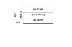
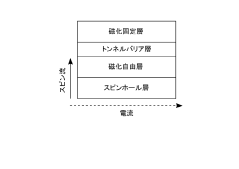
Spin injection source, magnetic memory, spin hall oscillator, computer, and magnetic sensor
PatentActiveJP2023034867A
Innovation
- A spin injection source using a half-Heusler alloy topological semimetal (HHA-TSM) with a Dirac-type surface state, which supplies a spin current to ferromagnetic materials, reducing the required current and maintaining structural integrity during semiconductor processing.
Exfoliation of thermoelectric materials and transition metal dichalcogenides using ionic liquids
PatentInactiveUS20150004733A1
Innovation
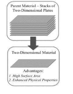
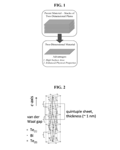
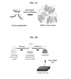
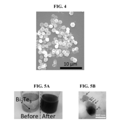
- The use of ionic liquids to exfoliate thermoelectric materials and transition metal dichalcogenides into two-dimensional or quasi-two-dimensional materials, such as quintuple sheets, which can be incorporated into printable inks for various applications, enhancing their thermoelectric properties and efficiency.
Materials Fabrication and Characterization Techniques
The fabrication of topological materials for spintronics applications requires sophisticated techniques to ensure high-quality samples with well-defined topological properties. Molecular Beam Epitaxy (MBE) stands as the premier method for growing Dirac and Weyl semimetal thin films, offering atomic-level precision and exceptional purity. This technique enables the growth of crystalline layers with minimal defects, critical for preserving the delicate topological states that underpin spin-dependent transport phenomena.
Chemical Vapor Deposition (CVD) represents another vital fabrication approach, particularly valuable for scaling production of topological materials. Recent advancements in CVD have enabled the synthesis of Weyl semimetals with controlled stoichiometry and crystal orientation, factors that significantly influence spin-orbit coupling strength and topological protection mechanisms.
Pulsed Laser Deposition (PLD) has emerged as an effective technique for creating heterostructures combining topological materials with conventional magnetic layers. The ability to precisely control interfaces at the nanoscale is crucial for engineering spin-transfer efficiency and manipulating magnetic proximity effects in next-generation spintronic devices.
For characterization, Angle-Resolved Photoemission Spectroscopy (ARPES) remains the gold standard for directly visualizing the electronic band structure of topological materials. Advanced spin-resolved ARPES variants can now map spin textures across momentum space, providing essential insights into the spin-momentum locking mechanisms that enable efficient spin current generation in these materials.
Scanning Tunneling Microscopy/Spectroscopy (STM/STS) offers complementary capabilities for probing local electronic states with atomic resolution. Recent developments in spin-polarized STM have enabled direct visualization of topological surface states and their interaction with magnetic dopants, critical for understanding interfacial spin phenomena.
Transport measurements under varying magnetic fields and temperatures provide crucial functional characterization. Hall effect measurements, magnetoresistance studies, and spin-torque ferromagnetic resonance techniques collectively enable quantification of spin-orbit torques, spin Hall angles, and spin diffusion lengths—key parameters for device applications.
Advanced synchrotron-based techniques, including X-ray magnetic circular dichroism (XMCD) and resonant inelastic X-ray scattering (RIXS), offer element-specific probes of magnetic properties and excitations. These techniques have proven invaluable for understanding the interplay between topological states and magnetism in complex material systems designed for spintronic applications.
Quantum Computing Integration Possibilities
The integration of topological materials, particularly Dirac and Weyl semimetals, with quantum computing represents a frontier with transformative potential for both fields. These materials' unique electronic properties—specifically their robust topological protection against decoherence—make them promising candidates for quantum bit (qubit) implementations that could overcome current stability limitations.
Quantum computing architectures could leverage the spin-momentum locking in topological materials to create more resilient qubits. The non-trivial Berry phase and topologically protected surface states in Dirac and Weyl semimetals offer natural protection against environmental perturbations, potentially extending coherence times—a critical metric for quantum computation.
Several integration pathways are emerging. Topological quantum computing, which utilizes non-Abelian anyons for topologically protected quantum operations, could benefit from Weyl semimetals' exotic quasiparticle excitations. These materials might serve as platforms for Majorana fermions, which are theoretically ideal for fault-tolerant quantum computing.
Hybrid quantum systems combining conventional superconducting qubits with topological material elements represent another promising direction. Such hybrids could utilize the best properties of both technologies—the established control mechanisms of superconducting circuits and the inherent protection of topological states.
For quantum memory applications, the persistent spin textures in certain topological materials could enable longer storage times for quantum information. The spin-orbit coupling characteristics that define these materials may allow for electrical manipulation of quantum states without magnetic fields, simplifying control architectures.
Experimental progress has already demonstrated coherent manipulation of surface states in topological insulators adjacent to superconductors, suggesting viable pathways toward topological qubit realization. Companies including Microsoft and Intel have invested significantly in topological quantum computing research, recognizing its disruptive potential.
Challenges remain substantial, however. The precise engineering of material interfaces, maintaining quantum coherence during operations, and developing reliable readout mechanisms for topologically encoded information all require breakthrough solutions. Additionally, theoretical work must advance to fully map the computational capabilities of topological quantum systems and develop appropriate algorithms.
The timeline for practical integration likely extends 5-10 years for proof-of-concept demonstrations, with commercially viable systems potentially emerging in the 15-20 year timeframe, contingent upon continued materials science advances and quantum engineering breakthroughs.
Unlock deeper insights with Patsnap Eureka Quick Research — get a full tech report to explore trends and direct your research. Try now!
Generate Your Research Report Instantly with AI Agent
Supercharge your innovation with Patsnap Eureka AI Agent Platform!