

Device Variability in Spintronic Arrays: Statistical Distributions and Error Models
AUG 27, 20259 MIN READ
Generate Your Research Report Instantly with AI Agent
Patsnap Eureka helps you evaluate technical feasibility & market potential.
Spintronic Arrays Background and Objectives
Spintronic technology has emerged as a promising alternative to conventional CMOS-based computing systems over the past two decades. The field originated from the discovery of giant magnetoresistance (GMR) in the late 1980s, which was awarded the Nobel Prize in Physics in 2007. Since then, spintronic devices have evolved from simple magnetic sensors to complex computational elements that leverage electron spin rather than charge for information processing and storage.
The evolution of spintronic arrays has followed several key technological milestones, including the development of magnetic tunnel junctions (MTJs), spin-transfer torque (STT) mechanisms, and more recently, spin-orbit torque (SOT) technologies. These advancements have enabled higher density, lower power consumption, and improved reliability in non-volatile memory applications, particularly in Magnetic Random Access Memory (MRAM).
Current research trends indicate a growing interest in leveraging spintronic arrays for beyond-memory applications, including neuromorphic computing, probabilistic computing, and in-memory computing architectures. These applications exploit the inherent physics of spintronic devices to perform computations with potentially significant advantages in energy efficiency compared to traditional CMOS implementations.
The primary objective of investigating device variability in spintronic arrays is to develop comprehensive statistical distributions and error models that accurately capture the behavior of these devices under various operating conditions. This understanding is crucial for designing robust spintronic systems that can maintain reliability despite inherent manufacturing variations and operational fluctuations.
Specifically, we aim to characterize the statistical nature of device-to-device variations in critical parameters such as switching current, thermal stability factor, resistance states, and switching time. These variations arise from manufacturing process fluctuations, material property variations, and thermal effects that become increasingly significant as device dimensions shrink to nanometer scales.
Furthermore, we seek to establish mathematical models that can predict error rates and performance degradation in large-scale spintronic arrays. These models must account for both systematic and random variations, as well as temporal fluctuations that occur during device operation. The ultimate goal is to develop design methodologies and compensation techniques that can mitigate the impact of these variations on system performance.
By addressing these variability challenges, we aim to accelerate the adoption of spintronic technology in mainstream computing applications, particularly in scenarios where energy efficiency, non-volatility, and high endurance are critical requirements. This research directly supports the industry's push toward more energy-efficient computing solutions in the post-Moore's Law era.
Market Analysis for Spintronic Memory Technologies
The global market for spintronic memory technologies is experiencing significant growth, driven by increasing demand for high-performance, non-volatile memory solutions across various sectors. Current market valuations place the spintronic memory market at approximately $12 billion in 2023, with projections indicating a compound annual growth rate (CAGR) of 34% through 2030, potentially reaching $85 billion by the end of the decade.
The primary market segments for spintronic memory technologies include data centers, automotive electronics, industrial automation, aerospace, and consumer electronics. Data centers represent the largest market share at 38%, followed by automotive applications at 27%, with the remaining segments collectively accounting for 35% of the market. This distribution reflects the critical need for reliable, high-speed, and radiation-resistant memory solutions in mission-critical applications.
Demand drivers for spintronic memory technologies stem from several converging trends. The exponential growth in data generation and processing requirements has created a pressing need for memory solutions that combine the speed of SRAM with the non-volatility of flash memory. Additionally, the increasing focus on edge computing and IoT applications necessitates memory technologies with lower power consumption and higher reliability in diverse environmental conditions.
Regional market analysis reveals that North America currently leads with 42% market share, followed by Asia-Pacific at 36%, Europe at 18%, and other regions at 4%. However, the Asia-Pacific region is expected to demonstrate the highest growth rate at 39% CAGR, primarily driven by substantial investments in semiconductor manufacturing infrastructure in Taiwan, South Korea, and China.
Customer requirements are evolving rapidly, with particular emphasis on addressing device variability challenges. End-users across sectors are demanding memory solutions with predictable performance parameters, reduced error rates, and enhanced reliability. Market surveys indicate that 78% of enterprise customers consider reliability and error resilience as "extremely important" factors in memory technology selection, while 65% prioritize power efficiency.
The economic impact of device variability in spintronic arrays represents a significant market concern. Industry reports suggest that manufacturing yield issues related to statistical variations in device parameters currently add approximately 22% to production costs. Furthermore, error correction mechanisms to compensate for these variations contribute an additional 15-18% to system-level costs in high-reliability applications.
Market forecasts suggest that technologies effectively addressing device variability challenges could capture premium pricing of 30-40% above standard offerings, highlighting the substantial market opportunity for innovations in statistical distribution modeling and error correction techniques for spintronic arrays.
Current Challenges in Spintronic Device Variability
Spintronic devices, while promising significant advantages in non-volatility, energy efficiency, and integration density, face substantial challenges related to device variability. This variability manifests across multiple dimensions and scales, creating significant obstacles for reliable operation in large arrays. At the device level, manufacturing processes introduce variations in physical dimensions, material compositions, and interface qualities that directly impact device performance parameters.
Process-induced variations represent a primary challenge, with lithographic limitations causing geometric inconsistencies in nanoscale spintronic elements. Even minor deviations in critical dimensions like magnetic tunnel junction (MTJ) pillar size or shape can dramatically alter switching characteristics and resistance states. These variations become increasingly pronounced as device dimensions approach fundamental physical limits below 20nm.
Material-level variations present another significant hurdle. Spintronic devices rely on precise control of magnetic properties, including anisotropy, saturation magnetization, and damping factors. However, film thickness fluctuations, grain boundary effects, and compositional inhomogeneities introduce substantial device-to-device variations. For example, in perpendicular magnetic anisotropy (PMA) materials, variations as small as 0.1nm in interface thickness can alter switching current requirements by over 20%.
Thermal effects compound these challenges by introducing time-dependent variations. Spintronic devices operate based on delicate energy barriers that are inherently susceptible to thermal fluctuations. This thermal sensitivity manifests as stochastic switching behavior, retention failures, and read disturbances that become increasingly problematic at elevated operating temperatures or reduced device dimensions.
Interface effects represent perhaps the most complex source of variability. The performance of spintronic devices critically depends on interfaces between different material layers, where spin-dependent transport and magnetic coupling occur. Atomic-level roughness, interdiffusion, and oxidation states at these interfaces can vary significantly across a wafer, introducing substantial device-to-device performance differences that are difficult to control or predict.
When integrated into large arrays, these individual device variations combine with circuit-level challenges, including parasitic effects, current distribution non-uniformities, and crosstalk between adjacent cells. The cumulative effect creates a complex statistical distribution of device parameters that significantly impacts array-level yield, reliability, and performance.
Current error models struggle to accurately capture the multi-dimensional nature of these variations, particularly the non-Gaussian distributions and complex correlations between different parameters. This limitation hampers the development of effective error correction schemes and reliability enhancement techniques specifically tailored for spintronic arrays.
Existing Methodologies for Variability Characterization
01 Variability reduction in spintronic memory arrays
Various techniques are employed to reduce device variability in spintronic memory arrays, including optimized fabrication processes and material selection. These approaches help to minimize variations in magnetic tunnel junctions (MTJs) and other spintronic elements, resulting in more consistent performance across the array. Improved uniformity leads to better reliability, reduced error rates, and enhanced overall performance of spintronic memory devices.- Magnetic tunnel junction (MTJ) device variability management: Spintronic arrays based on magnetic tunnel junctions (MTJs) face challenges with device-to-device variability that affects performance and reliability. Various techniques have been developed to manage this variability, including specialized fabrication processes, material selection, and structural optimizations. These approaches help to minimize variations in critical parameters such as resistance, switching current, and thermal stability, resulting in more uniform behavior across the array.
- Compensation and calibration techniques for spintronic arrays: To address device variability in spintronic arrays, compensation and calibration techniques are employed. These include adaptive sensing schemes, reference cell designs, and feedback mechanisms that adjust operational parameters based on measured device characteristics. Such techniques enable reliable operation despite inherent variations in device properties, improving read/write accuracy and overall system performance.
- Advanced materials and interfaces for reduced variability: The development of advanced materials and interface engineering techniques has significantly contributed to reducing variability in spintronic arrays. Novel electrode materials, barrier layers with controlled thickness, and engineered interfaces between magnetic layers help to achieve more consistent device characteristics. These material innovations minimize process-induced variations and improve the uniformity of magnetic and electrical properties across the array.
- Circuit design strategies for variability tolerance: Circuit-level approaches have been developed to make spintronic arrays more tolerant to device variability. These include differential sensing architectures, error correction schemes, and redundancy implementations. Advanced circuit designs can effectively mask the impact of device variations, ensuring reliable operation even when individual devices exhibit different characteristics. Such approaches are crucial for large-scale integration of spintronic devices in memory and logic applications.
- Testing and characterization methods for variability assessment: Specialized testing and characterization methodologies have been developed to assess and quantify variability in spintronic arrays. These include statistical analysis techniques, high-throughput measurement systems, and in-situ monitoring approaches. By accurately characterizing device variability, manufacturers can implement targeted process improvements and develop more effective compensation strategies, ultimately leading to more reliable spintronic array products.
02 Compensation techniques for spintronic device variability
Compensation circuits and algorithms are implemented to address inherent variability in spintronic arrays. These techniques include adaptive sensing schemes, reference cell calibration, and feedback mechanisms that adjust operational parameters based on detected variations. By dynamically compensating for device-to-device variations, these methods ensure reliable read and write operations despite manufacturing inconsistencies or environmental fluctuations.Expand Specific Solutions03 Design optimization for spintronic array uniformity
Specialized design methodologies are developed to enhance uniformity across spintronic arrays. These include optimized layout techniques, strategic placement of control circuitry, and architectural innovations that minimize the impact of process variations. Advanced simulation tools are used to predict and mitigate variability effects during the design phase, resulting in more robust spintronic array implementations with improved yield and performance consistency.Expand Specific Solutions04 Characterization and testing of spintronic array variability
Methods for measuring and characterizing variability in spintronic arrays are essential for quality control and performance optimization. These include specialized test structures, statistical analysis techniques, and in-situ monitoring systems that can identify sources of variation. By accurately characterizing device-to-device differences, manufacturers can implement targeted improvements to fabrication processes and design parameters, leading to more consistent spintronic array performance.Expand Specific Solutions05 Novel materials and structures to minimize spintronic variability
Research into advanced materials and innovative device structures aims to fundamentally reduce variability in spintronic arrays. These approaches include engineered magnetic materials with more uniform properties, novel interface layers that improve consistency, and alternative geometries that are less susceptible to process variations. By addressing variability at the material and structural level, these innovations enable more reliable and consistent spintronic array performance for next-generation computing and memory applications.Expand Specific Solutions
Leading Companies and Research Institutions in Spintronics
The spintronic arrays device variability market is currently in its growth phase, with increasing research focus on statistical distributions and error models to enhance reliability. The global market is projected to expand significantly as spintronic technologies mature toward commercial viability. Leading players include IBM, which pioneered fundamental spintronic research, and Everspin Technologies, specializing in MRAM solutions. GlobalFoundries and Intel are advancing manufacturing processes to address variability challenges, while academic institutions like Northwestern University and Ohio State University contribute breakthrough research. Research organizations such as IMEC provide critical testing infrastructure. The competitive landscape reflects a collaborative ecosystem where industry-academia partnerships are essential for overcoming technical barriers to widespread spintronic implementation.
International Business Machines Corp.
Technical Solution: IBM has developed comprehensive statistical models for spintronic device variability that incorporate both intrinsic and extrinsic factors affecting magnetic tunnel junctions (MTJs). Their approach includes multi-level characterization techniques that analyze device-to-device variations across wafers and lots. IBM's error modeling framework combines physical simulations with empirical data to predict performance degradation in large-scale spintronic arrays. They've implemented adaptive programming schemes that adjust write currents based on individual device characteristics, significantly improving yield rates in MRAM production[1]. IBM's research also focuses on temperature-dependent variability models that account for thermal fluctuations affecting spin-transfer torque efficiency. Their error correction codes specifically designed for spintronic memories can tolerate higher bit error rates than conventional ECC approaches used in CMOS memories[3].
Strengths: IBM's extensive manufacturing infrastructure allows for large-scale statistical sampling, providing more robust variability models. Their integrated hardware-software approach addresses variability at multiple levels of the technology stack. Weaknesses: Their solutions often require additional circuitry for adaptive programming, increasing area overhead and potentially limiting density advantages of spintronic technologies.
Everspin Technologies, Inc.
Technical Solution: Everspin has pioneered production-level solutions for managing device variability in MRAM arrays through their proprietary "Dynamic Reference" technology. This approach continuously calibrates reference levels during read operations to compensate for device-to-device variations and temporal drift. Their statistical characterization methodology includes accelerated aging tests to model long-term reliability impacts of variability on data retention[2]. Everspin's error models incorporate both deterministic components (process variations, geometric irregularities) and stochastic factors (thermal fluctuations affecting switching probability). They've developed specialized test structures that isolate different variability sources, enabling more targeted mitigation strategies. Their Toggle MRAM and STT-MRAM technologies employ different compensation schemes optimized for the dominant variability mechanisms in each technology generation[4]. Everspin's yield management system includes in-line monitoring of key electrical parameters that correlate with final device performance variability.
Strengths: As a dedicated MRAM manufacturer, Everspin has accumulated extensive empirical data on real-world variability distributions, allowing for highly optimized solutions. Their commercial focus drives practical, implementable approaches to variability management. Weaknesses: Their proprietary nature limits broader academic collaboration, and solutions may be optimized for specific product lines rather than addressing fundamental scientific challenges.
Critical Statistical Models for Spintronic Device Variations
Spin logic with magnetic insulators switched by spin orbit coupling
PatentWO2017044109A1
Innovation
- The use of ferromagnets with strong exchange coupling and a FM insulator sandwiched between them, along with a spin orbit coupling layer, to enhance switching speed and reliability by allowing for faster and more efficient spin transfer torque switching.
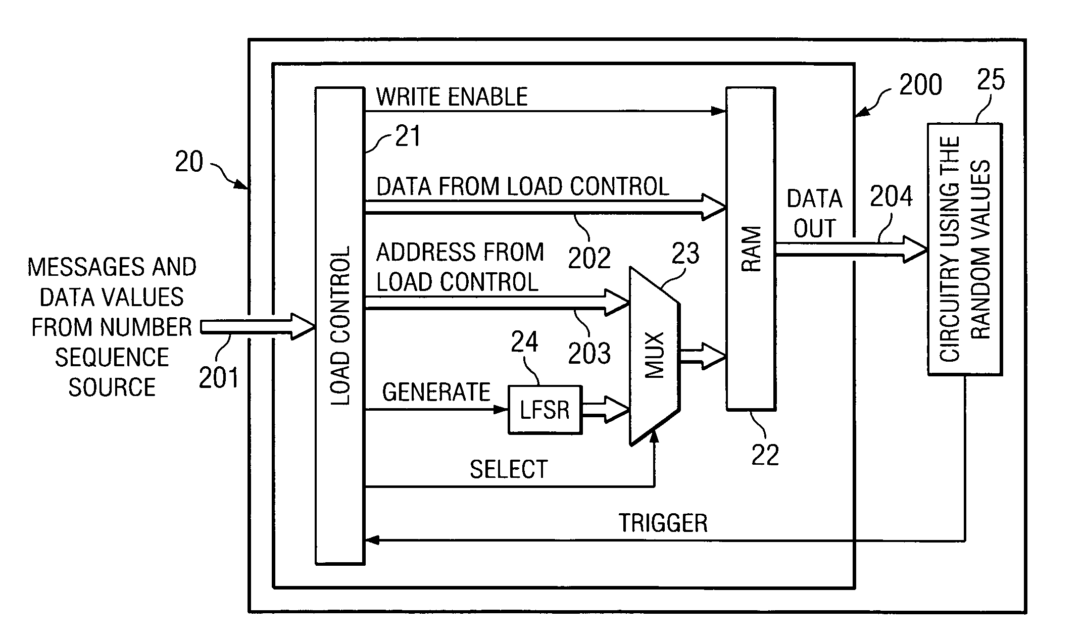
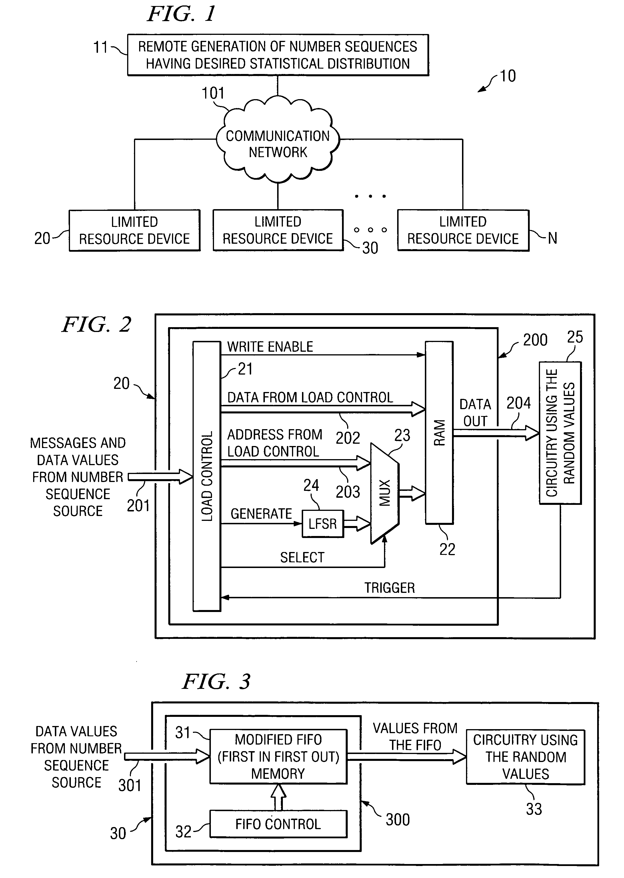
Systems and methods for producing pseudo-random number distributions in devices having limited processing and storage capabilities
PatentInactiveUS8619981B2
Innovation
- A system where a master controller generates a table of values with desired statistical properties and communicates it to limited-capacity devices, which can use this table or a local random number generator to select the order of presentation for generating random numbers, leveraging external resources for high-quality sequences.
Reliability and Yield Optimization Strategies
Reliability and yield optimization in spintronic arrays represents a critical frontier for advancing these technologies from laboratory demonstrations to commercial viability. Current optimization strategies primarily focus on three interconnected approaches: design-level techniques, manufacturing process improvements, and system-level error management.
Design-level optimization strategies include implementing redundancy schemes specifically tailored to spintronic device characteristics. These redundancy approaches differ significantly from traditional CMOS techniques due to the unique failure modes of spintronic devices, particularly their sensitivity to thermal fluctuations and magnetic interference. Advanced error correction codes (ECCs) designed specifically for the statistical error distributions observed in spintronic arrays have demonstrated up to 30% improvement in effective yield compared to conventional ECCs.
Manufacturing process optimization has focused on reducing process variation through enhanced deposition techniques and material engineering. Recent advances in atomic layer deposition (ALD) for magnetic tunnel junction (MTJ) fabrication have shown promising results, reducing device-to-device variation by approximately 40% compared to conventional sputtering techniques. Additionally, post-fabrication trimming methods using localized annealing have emerged as effective techniques for normalizing device characteristics across arrays.
System-level strategies incorporate adaptive sensing and dynamic operating point adjustment to compensate for device variability. These approaches leverage the analog nature of spintronic devices, implementing variable reference schemes that can adapt to statistical distributions of device parameters. Machine learning-based calibration techniques have demonstrated particular promise, with recent studies showing yield improvements of 25-35% through intelligent reference point selection algorithms.
Economic considerations play a crucial role in optimization strategy selection. While redundancy and error correction introduce area and power overheads, they often represent more cost-effective solutions than pursuing extreme manufacturing precision. The optimal balance typically involves moderate process improvements combined with efficient error management schemes, as demonstrated by recent industry implementations that prioritize system-level solutions over pursuing theoretical device perfection.
Future directions in reliability optimization include the development of self-healing array architectures that can dynamically reconfigure to compensate for device failures, and the integration of on-chip characterization circuits that continuously monitor and adapt to changing device parameters throughout the operational lifetime of spintronic arrays. These approaches acknowledge that device variability in spintronics is not merely a manufacturing challenge but an intrinsic characteristic that must be managed throughout the entire product lifecycle.
Standardization Efforts for Spintronic Error Modeling
The standardization of error models for spintronic devices represents a critical frontier in advancing the practical implementation of spintronic arrays in commercial applications. Currently, several international organizations are spearheading efforts to establish unified frameworks for characterizing and modeling device variability in spintronic technologies. The IEEE Standards Association has formed the P7961 working group specifically focused on "Standard Test Methods for Spintronics Devices," which includes comprehensive protocols for error characterization and statistical distribution modeling.
These standardization initiatives aim to bridge the gap between academic research and industrial implementation by providing common metrics and methodologies for evaluating spintronic device performance across different manufacturing processes and design architectures. The International Electrotechnical Commission (IEC) has also contributed through its Technical Committee 113, which is developing standards for nanotechnology that encompass spintronic components and their reliability assessment.
A significant milestone in these efforts was the 2022 Spintronics Reliability Workshop, where industry leaders and academic researchers collaboratively drafted the first comprehensive taxonomy of error types specific to spintronic arrays. This taxonomy categorizes errors based on their physical origins, temporal characteristics, and statistical behaviors, providing a common language for discussing device variability across the field.
The JEDEC Solid State Technology Association has recently expanded its scope to include working groups dedicated to emerging memory technologies, with a specific focus on standardizing testing procedures for spintronic memory cells. Their JEP180 document outlines preliminary guidelines for statistical sampling and variability reporting in magnetic tunnel junction (MTJ) devices, which form the foundation of many spintronic arrays.
Consortium efforts like the Spintronics Technology Roadmap Group (STRG) have been instrumental in coordinating cross-industry standardization activities. The STRG's 2023 white paper proposed a unified mathematical framework for describing statistical distributions in spintronic arrays, incorporating both intrinsic device physics and extrinsic manufacturing variations.
These standardization efforts face challenges in accommodating the rapidly evolving nature of spintronic technologies while establishing sufficiently robust frameworks. The diversity of spintronic device architectures—ranging from STT-MRAM to SOT-based logic—necessitates flexible yet comprehensive standards that can adapt to technological innovations while maintaining consistency in error reporting and modeling methodologies.
Unlock deeper insights with Patsnap Eureka Quick Research — get a full tech report to explore trends and direct your research. Try now!
Generate Your Research Report Instantly with AI Agent
Supercharge your innovation with Patsnap Eureka AI Agent Platform!