Radiation-Hardened Spintronic Memories for Aerospace Applications
AUG 27, 20259 MIN READ
Generate Your Research Report Instantly with AI Agent
Patsnap Eureka helps you evaluate technical feasibility & market potential.
Spintronic Memory Technology Background and Objectives
Spintronic memory technology represents a revolutionary advancement in non-volatile memory systems, emerging from the field of spintronics which exploits the intrinsic spin of electrons alongside their charge properties. The evolution of this technology can be traced back to the discovery of giant magnetoresistance (GMR) in the late 1980s, which earned Albert Fert and Peter Grünberg the Nobel Prize in Physics in 2007. This fundamental breakthrough laid the groundwork for subsequent developments in magnetic random-access memory (MRAM) and spin-transfer torque MRAM (STT-MRAM).
The technological trajectory has been marked by significant milestones, including the commercialization of first-generation MRAM devices in the early 2000s, followed by more advanced STT-MRAM products in the 2010s. Recent innovations have focused on spin-orbit torque (SOT) mechanisms and voltage-controlled magnetic anisotropy (VCMA), pushing the boundaries of energy efficiency and operational speed.
In aerospace applications, memory systems face extreme environmental challenges, particularly radiation exposure which can cause single-event upsets (SEUs), total ionizing dose (TID) effects, and displacement damage. Conventional semiconductor memories like DRAM and flash exhibit vulnerability to these radiation effects, necessitating complex error correction codes and redundancy schemes that increase system complexity and power consumption.
Spintronic memories offer inherent advantages for radiation-hardened applications due to their fundamental physics. The magnetic storage mechanism is inherently less susceptible to radiation-induced charge displacement compared to charge-based storage in conventional memories. This intrinsic radiation hardness makes spintronic technologies particularly promising for aerospace systems operating in harsh radiation environments such as satellite systems, deep space probes, and high-altitude aircraft.
The primary technical objectives for radiation-hardened spintronic memories include achieving radiation tolerance levels exceeding 300 krad (Si) for TID effects and immunity to SEUs at linear energy transfer (LET) values above 60 MeV-cm²/mg. Additional goals encompass maintaining reliable operation across the extreme temperature ranges encountered in aerospace environments (-55°C to +125°C), while simultaneously reducing power consumption by at least 50% compared to current radiation-hardened memory solutions.
Furthermore, the technology aims to achieve write endurance exceeding 10^12 cycles and data retention periods of over 10 years, ensuring long-term reliability for mission-critical aerospace systems. Scalability to advanced process nodes (28nm and below) represents another crucial objective to enable higher density integration and support the increasing data processing requirements of modern aerospace applications.
Aerospace Market Demand for Radiation-Hardened Memory
The aerospace industry has witnessed a significant surge in demand for radiation-hardened memory solutions over the past decade. This demand is primarily driven by the increasing complexity of space missions, longer operational lifetimes of satellites, and the growing commercial space sector. Traditional memory technologies such as DRAM and Flash memory are highly susceptible to radiation effects in space environments, leading to data corruption, system failures, and reduced mission reliability.
Market analysis indicates that the global radiation-hardened electronics market, including memory components, is projected to reach $1.6 billion by 2025, with a compound annual growth rate of approximately 3.7%. Within this market, radiation-hardened memory represents a critical segment with particularly strong growth prospects due to the expanding satellite constellation deployments for global internet coverage and Earth observation missions.
The commercial space sector, led by companies like SpaceX, Blue Origin, and numerous small satellite manufacturers, has emerged as a significant driver for radiation-hardened memory solutions. These companies are launching satellite constellations numbering in the hundreds to thousands of units, each requiring reliable memory systems capable of withstanding the harsh radiation environment of space.
Government space agencies, including NASA, ESA, JAXA, and others, continue to represent a substantial portion of the market demand. Their deep space exploration missions, lunar and Mars initiatives, and scientific satellites require increasingly sophisticated onboard computing capabilities with radiation-tolerant memory systems offering higher densities and lower power consumption than previous generations.
Military and defense applications constitute another major market segment, with requirements for radiation-hardened memory in military satellites, reconnaissance systems, and communication networks. These applications often demand the highest reliability standards and can tolerate premium pricing for guaranteed performance in extreme environments.
The market shows a clear trend toward higher memory densities, with current requirements typically in the gigabit range compared to megabit-scale solutions from a decade ago. This escalation reflects the growing complexity of onboard data processing, autonomous operation capabilities, and the increasing volume of scientific and imaging data collected during missions.
Power efficiency has emerged as a critical market requirement, as modern spacecraft designs often face strict power budgets. This has created specific demand for radiation-hardened memory solutions that not only survive in radiation environments but also maintain competitive power consumption profiles compared to their commercial counterparts.
Cost considerations are increasingly important as the commercial space sector grows. While government and military customers can often absorb the premium costs associated with radiation-hardened components, commercial satellite manufacturers seek more cost-effective solutions that balance radiation tolerance with economic viability for large-scale deployments.
Current Challenges in Radiation-Hardened Memory Technologies
The aerospace industry faces significant challenges in developing memory technologies that can withstand the harsh radiation environment of space. Traditional semiconductor-based memories such as SRAM, DRAM, and Flash are highly susceptible to radiation effects, including Single Event Upsets (SEUs), Single Event Functional Interrupts (SEFIs), and Total Ionizing Dose (TID) damage. These radiation effects can cause bit flips, data corruption, and even permanent device failure, compromising mission-critical systems.
Current radiation-hardened memory solutions primarily rely on redundancy techniques, error correction codes (ECC), and specialized manufacturing processes. However, these approaches often result in significant penalties in terms of area overhead, power consumption, and performance degradation. For instance, Triple Modular Redundancy (TMR) requires three times the silicon area, while ECC implementations add latency to memory operations and increase complexity.
The scaling limitations of traditional CMOS-based radiation-hardened memories present another major challenge. As feature sizes decrease to improve density and performance, the susceptibility to radiation effects increases exponentially. This creates a fundamental trade-off between advanced performance characteristics and radiation hardness that is becoming increasingly difficult to balance with conventional technologies.
Power constraints represent a critical challenge for space applications, where energy resources are strictly limited. Current radiation-hardened memories typically consume significantly more power than their commercial counterparts due to their protective design features. This power overhead restricts operational capabilities and mission duration for space systems, particularly in small satellites and deep space probes.
Temperature stability across extreme ranges (-55°C to +125°C and beyond) remains problematic for existing radiation-hardened memories. Space environments experience dramatic temperature fluctuations, and memory technologies must maintain reliable operation and data retention across these conditions. Current solutions often exhibit compromised performance at temperature extremes.
Manufacturing complexity and cost present substantial barriers to widespread adoption of radiation-hardened memories. Specialized fabrication processes, extensive testing requirements, and low production volumes result in costs that can be 10-100 times higher than commercial alternatives. This economic challenge limits innovation and restricts the deployment of advanced memory technologies in space systems.
Reliability verification and qualification standards for radiation-hardened memories involve lengthy and expensive testing procedures. The lack of standardized testing methodologies across different space agencies and manufacturers further complicates the development and certification process, extending time-to-market and increasing development costs for new memory technologies.
Current Spintronic Solutions for Radiation Environments
01 Radiation-hardened spintronic memory designs
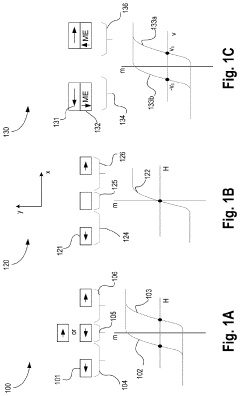
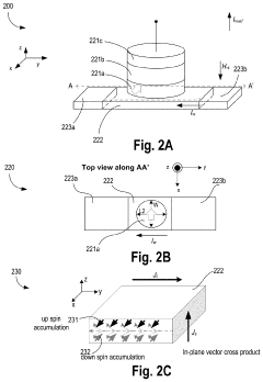
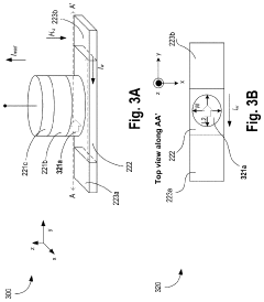
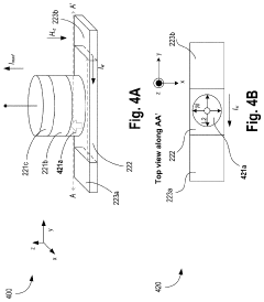
Specific design architectures for spintronic memories that enhance radiation hardness through structural modifications. These designs incorporate specialized circuit configurations, shielding layers, and redundant memory cells to mitigate radiation effects. The radiation-hardened designs maintain data integrity and operational stability in high-radiation environments while preserving the inherent advantages of spintronic technology such as non-volatility and low power consumption.- Radiation-hardened spintronic memory designs: Specialized design architectures for spintronic memories that inherently resist radiation effects. These designs incorporate specific circuit configurations and material choices that minimize susceptibility to single event upsets and total ionizing dose effects. The structures often include redundant elements or specialized shielding layers that protect the magnetic tunnel junctions from radiation-induced damage while maintaining data integrity in harsh environments.
- Magnetic tunnel junction (MTJ) structures for radiation tolerance: Advanced MTJ structures that form the core of radiation-hardened spintronic memories. These structures utilize specific material compositions and layer arrangements to enhance radiation tolerance while maintaining desirable magnetic properties. The designs often feature specialized free layers, reference layers, and tunnel barriers that resist state changes when exposed to radiation, ensuring data retention in high-radiation environments.
- Circuit techniques for radiation hardening in spintronic devices: Circuit-level approaches to enhance radiation tolerance in spintronic memory systems. These techniques include specialized sensing circuits, error correction mechanisms, and redundant storage elements that can detect and mitigate radiation-induced errors. The circuits often incorporate differential sensing, reference cell designs, and specialized read/write mechanisms that maintain proper operation even when exposed to radiation events.
- Integration methods for radiation-hardened spintronic memories: Fabrication and integration techniques specifically developed for radiation-hardened spintronic memory systems. These methods focus on process modifications, material selections, and integration approaches that enhance radiation tolerance while maintaining manufacturability. The techniques often include specialized deposition methods, annealing processes, and encapsulation strategies that protect the sensitive magnetic elements from radiation damage throughout the device lifetime.
- Testing and qualification methods for radiation-hardened spintronic memories: Specialized testing protocols and qualification methodologies developed for evaluating the radiation hardness of spintronic memory devices. These methods include accelerated radiation testing, simulation approaches, and analytical techniques to predict and verify performance in radiation environments. The approaches often incorporate specialized test structures, measurement techniques, and qualification standards specifically designed for spintronic technologies in space, military, and nuclear applications.
02 Materials for radiation-resistant spintronic devices
Advanced materials and compositions specifically developed for radiation-resistant spintronic memory applications. These materials include specialized magnetic layers, tunnel barriers, and electrode materials that demonstrate enhanced stability under radiation exposure. The materials are engineered at the atomic level to resist displacement damage, ionization effects, and other radiation-induced phenomena while maintaining their magnetic and electronic properties essential for spintronic operation.Expand Specific Solutions03 Circuit techniques for radiation immunity
Electronic circuit techniques implemented in spintronic memory systems to provide radiation immunity. These include specialized sensing circuits, error correction mechanisms, and radiation-tolerant peripheral circuits that work together with the inherent radiation resistance of magnetic storage elements. The circuit approaches focus on detecting and mitigating radiation-induced transient effects, preventing error propagation, and ensuring reliable read/write operations in radiation environments.Expand Specific Solutions04 Integration methods for radiation-hardened spintronic memories
Fabrication and integration techniques for incorporating radiation-hardened spintronic memories into semiconductor devices and systems. These methods address the challenges of combining magnetic materials with traditional semiconductor processes while maintaining radiation tolerance. The integration approaches include specialized deposition techniques, thermal management strategies, and isolation methods that preserve the radiation-hardening features throughout the manufacturing process.Expand Specific Solutions05 Testing and qualification of radiation-hardened spintronic memories
Methods and systems for testing, qualifying, and characterizing the radiation hardness of spintronic memory devices. These include specialized test structures, radiation exposure protocols, and performance metrics specifically developed for evaluating spintronic technologies in radiation environments. The testing approaches enable accurate prediction of device performance and reliability in space, nuclear, and other high-radiation applications, allowing for proper qualification before deployment.Expand Specific Solutions
Leading Companies in Aerospace Memory Systems
The radiation-hardened spintronic memory market for aerospace applications is currently in its growth phase, with increasing demand driven by the need for reliable data storage in harsh space environments. The global market is estimated to reach approximately $300-400 million by 2025, with a CAGR of 15-20%. Regarding technological maturity, established players like Everspin Technologies and Thales SA lead with commercial MRAM solutions, while Intel, Samsung, and Toshiba are advancing next-generation spintronic technologies. Research institutions including CNRS, McGill University, and the Institute of Microelectronics of CAS are developing fundamental innovations. Emerging companies such as Avalanche Technology and KIOXIA are focusing on specialized radiation-hardened solutions, while aerospace specialists like BAE Systems and Shanghai Satellite Equipment Research Institute are integrating these technologies into mission-critical systems.
Everspin Technologies, Inc.
Technical Solution: Everspin Technologies has developed Magnetoresistive Random Access Memory (MRAM) technology specifically engineered for radiation-hardened aerospace applications. Their Toggle MRAM and Spin-Transfer Torque MRAM (STT-MRAM) solutions leverage the inherent radiation resistance of magnetic tunnel junctions (MTJs), which store data as magnetic orientation rather than electrical charge. This approach eliminates the vulnerability to single-event upsets (SEUs) that plague conventional semiconductor memories. Everspin's radiation-hardened MRAMs maintain data integrity even when exposed to total ionizing dose (TID) levels exceeding 1 Mrad, making them suitable for satellite and deep space missions[1]. Their latest generation of aerospace-grade STT-MRAM offers densities up to 1Gb with read/write endurance exceeding 10^13 cycles while maintaining data retention periods of over 20 years at operating temperatures[2].
Strengths: Inherent radiation hardness without additional shielding; non-volatile operation eliminates standby power; high endurance compared to Flash memory; fast write speeds (35ns); proven flight heritage on multiple space missions. Weaknesses: Lower storage density compared to NAND Flash; higher cost per bit than conventional memories; requires specialized manufacturing processes; higher power consumption during write operations compared to SRAM.
Thales SA
Technical Solution: Thales has pioneered radiation-hardened spintronic memory solutions through their Space-grade Magnetic Random Access Memory (MRAM) program. Their approach combines proprietary radiation-hardened design techniques with specialized magnetic materials optimized for space environments. Thales' MRAM technology utilizes perpendicular magnetic tunnel junctions (p-MTJs) with synthetic antiferromagnetic reference layers that maintain stability under radiation exposure. Their radiation-hardened memory cells have demonstrated immunity to single-event effects (SEEs) up to linear energy transfer (LET) values of 120 MeV·cm²/mg, significantly outperforming conventional memories[3]. Thales has implemented redundancy schemes and error correction codes specifically designed for space applications, enabling their memories to withstand total ionizing doses exceeding 300 krad(Si) without performance degradation. Their latest generation of radiation-hardened MRAM achieves write speeds below 20ns while maintaining data retention at temperatures ranging from -55°C to +125°C, meeting stringent aerospace reliability requirements[4].
Strengths: Exceptional radiation tolerance without performance degradation; comprehensive space qualification testing completed; integrated error detection and correction capabilities; wide operating temperature range; low power consumption in standby mode. Weaknesses: Limited commercial availability compared to mainstream memory technologies; higher initial development costs; requires specialized testing facilities; integration challenges with some legacy aerospace systems.
Key Patents in Radiation-Hardened Spintronic Memory
Spin orbit memory with multiferroic material
PatentActiveUS20190386202A1
Innovation
- A two-terminal memory bit-cell utilizing multiferroic materials, where the write electrode comprises heavy metals or antiferromagnetic materials with large spin-orbit torque to switch magnetization, decoupling read and write operations and enabling low-power, high-density memory storage.
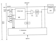
Apparatus and method of error detection and correction in a radiation-hardened static random access memory field-programmable gate array
PatentInactiveUS20040124876A1
Innovation
- A radiation-tolerant SRAM-based FPGA design incorporating error detection and correction circuitry, utilizing a background READ/WRITE scheme with Error Correction Code (ECC) bits to ensure data accuracy, and implementing triple-mode redundancy (TMR) and cyclic redundancy check (CRC) mechanisms to correct errors caused by SEUs.
Reliability Testing Standards for Aerospace Electronics
Reliability testing standards for aerospace electronics represent a critical framework for ensuring the performance and durability of radiation-hardened spintronic memories in extreme space environments. These standards are established by international organizations such as the European Space Agency (ESA), NASA, and the Department of Defense (DoD), providing comprehensive guidelines for qualifying electronic components for aerospace applications.
The primary aerospace reliability standards include MIL-STD-883 for microelectronic test methods, JEDEC JESD57 for stress-test-driven qualification, and ESCC 22900 for total ionizing dose testing. These standards specifically address radiation effects through tests like Single Event Effects (SEE) testing, Total Ionizing Dose (TID) testing, and Displacement Damage (DD) testing, which are particularly relevant for spintronic memories deployed in radiation-intensive environments.
For radiation-hardened spintronic memories, the testing protocols typically involve accelerated radiation exposure using particle accelerators or cobalt-60 gamma sources to simulate years of space radiation within compressed timeframes. The qualification process requires devices to maintain functionality after exposure to specified radiation levels, typically ranging from 100 krad to 1 Mrad for most aerospace applications, with military and deep space missions demanding even higher tolerance levels.
Temperature cycling tests represent another crucial aspect of reliability testing, with standards requiring spintronic memories to function across extreme temperature ranges from -55°C to +125°C. This is particularly important as spintronic devices exhibit temperature-dependent magnetic behavior that can affect data retention and switching characteristics in space environments.
Vibration and mechanical shock testing standards (MIL-STD-810) ensure that spintronic memory packages can withstand launch conditions and in-orbit mechanical stresses. These tests typically subject devices to random vibration profiles of 20-2000 Hz and shock pulses exceeding 1000g to verify structural integrity and continued electrical performance.
Recent updates to aerospace reliability standards have begun incorporating specific provisions for emerging technologies like spintronic memories. The JEDEC JC-13.5 committee has developed specialized test methods for magnetic memory technologies, addressing unique failure mechanisms such as magnetic field immunity and data retention under radiation exposure.
Compliance with these standards requires extensive documentation and traceability throughout the testing process. Manufacturers must maintain detailed records of test conditions, procedures, and results, often requiring third-party verification from certified testing laboratories. This rigorous approach ensures that radiation-hardened spintronic memories meet the exceptional reliability demands of aerospace applications where repair or replacement is impossible after deployment.
Cost-Performance Analysis of Spintronic vs. Traditional Solutions
When evaluating radiation-hardened spintronic memories for aerospace applications, cost-performance analysis becomes a critical factor in technology adoption decisions. Traditional radiation-hardened memory solutions, primarily based on SRAM and MRAM technologies, have historically dominated the aerospace sector due to their proven reliability. However, these solutions come with significant cost premiums, often 10-100 times the price of commercial equivalents, and performance limitations including lower density and speed.
Spintronic memory technologies offer compelling advantages in this cost-performance equation. The manufacturing processes for spintronic memories can leverage existing semiconductor fabrication infrastructure, potentially reducing production costs by 30-40% compared to specialized radiation-hardened traditional solutions. Additionally, the inherent radiation resistance of spintronic devices means less shielding and redundancy are required, further reducing system-level costs.
Performance metrics also favor spintronic solutions in radiation environments. While traditional radiation-hardened memories typically suffer 40-60% performance degradation compared to their commercial counterparts, spintronic memories maintain approximately 80-90% of their nominal performance under similar radiation conditions. This translates to higher data throughput and lower power consumption, critical factors for space-constrained aerospace systems with limited power budgets.
Total cost of ownership calculations reveal additional advantages. Spintronic memories demonstrate longer operational lifetimes in radiation environments, with projected mean time between failures (MTBF) 2-3 times higher than traditional solutions. This extended reliability reduces replacement frequency and associated mission costs, particularly relevant for long-duration space missions where component replacement is impossible.
Energy efficiency metrics further enhance the spintronic value proposition. Power consumption in spintronic memories is typically 40-60% lower than radiation-hardened SRAM solutions, reducing thermal management requirements and extending battery life in autonomous systems. This efficiency translates directly to reduced system weight and power supply requirements, factors that command premium costs in aerospace applications.
Market analysis indicates that while spintronic solutions currently carry a 15-25% price premium over non-hardened commercial memories, this gap is significantly smaller than the 300-500% premium commanded by traditional radiation-hardened solutions. As production volumes increase, this cost differential is expected to decrease further, potentially reaching price parity with commercial solutions within 5-7 years while maintaining superior radiation performance.
Unlock deeper insights with Patsnap Eureka Quick Research — get a full tech report to explore trends and direct your research. Try now!
Generate Your Research Report Instantly with AI Agent
Supercharge your innovation with Patsnap Eureka AI Agent Platform!