Energy Efficiency Benchmarks for Spintronic Memory Cells in AI Accelerators
AUG 27, 20259 MIN READ
Generate Your Research Report Instantly with AI Agent
Patsnap Eureka helps you evaluate technical feasibility & market potential.
Spintronic Memory Evolution and Objectives
Spintronic memory technology has evolved significantly over the past two decades, transitioning from theoretical concepts to practical implementations in various computing architectures. The journey began with the discovery of giant magnetoresistance (GMR) in the late 1980s, which laid the foundation for spintronic devices. This was followed by the development of magnetic tunnel junctions (MTJs) in the 1990s, which significantly improved signal-to-noise ratios and enabled more reliable data storage.
The evolution accelerated in the early 2000s with the introduction of spin-transfer torque (STT) mechanisms, allowing for more energy-efficient writing operations compared to field-induced switching. This breakthrough addressed one of the major limitations of early spintronic devices - high energy consumption during state changes. By 2010, perpendicular magnetic anisotropy (PMA) materials were integrated into MTJ structures, further reducing the critical current needed for switching while enhancing thermal stability.
Recent advancements have focused on voltage-controlled magnetic anisotropy (VCMA) and spin-orbit torque (SOT) technologies, which promise even lower energy consumption and faster switching speeds. These developments have positioned spintronic memory as a viable alternative to conventional CMOS-based memories, particularly for applications requiring non-volatility, high endurance, and energy efficiency.
The primary objective of current spintronic memory research is to establish comprehensive energy efficiency benchmarks specifically tailored for AI accelerator applications. This involves quantifying the energy consumption across various operations including read, write, and standby states under different workload conditions typical in neural network processing. Such benchmarks are crucial for comparing spintronic solutions against established technologies like SRAM, DRAM, and emerging alternatives.
Another key objective is to identify the optimal spintronic cell architecture for AI workloads, considering the unique access patterns and parallel processing requirements of neural network computations. This includes evaluating different configurations such as 1T-1MTJ, 2T-1MTJ, and cross-point arrays to determine which offers the best balance of density, speed, and energy efficiency.
Furthermore, research aims to establish scaling projections for spintronic memory technologies, mapping how energy efficiency metrics will evolve as device dimensions shrink to sub-20nm nodes. This forward-looking analysis is essential for determining the long-term viability of spintronic memory in future AI hardware generations, where energy constraints will become increasingly stringent.
The ultimate goal is to develop design guidelines that enable system architects to effectively integrate spintronic memory cells into AI accelerator designs, maximizing computational efficiency while minimizing energy consumption. This requires not only optimizing the memory cells themselves but also developing appropriate peripheral circuits and control schemes that leverage the unique characteristics of spintronic devices.
Market Analysis for Energy-Efficient AI Accelerators
The global market for energy-efficient AI accelerators is experiencing unprecedented growth, driven by the increasing deployment of AI applications across various sectors. Current market valuations indicate that the AI accelerator market reached approximately $8 billion in 2022 and is projected to grow at a CAGR of 38% through 2028, with energy efficiency emerging as a critical differentiating factor.
Demand for energy-efficient AI hardware is primarily fueled by data centers, which currently consume over 2% of global electricity. With AI workloads expected to account for 15-20% of total data center power consumption by 2025, the need for more efficient solutions is becoming urgent. Cloud service providers are increasingly prioritizing performance-per-watt metrics when selecting AI acceleration hardware.
The market segmentation reveals distinct customer profiles with varying energy efficiency requirements. Hyperscalers like Google, Amazon, and Microsoft are investing heavily in custom silicon solutions that maximize computational efficiency. Enterprise customers seek balanced solutions that offer both energy efficiency and compatibility with existing infrastructure. Edge computing applications demand ultra-low power consumption, creating a growing market for specialized accelerators with power envelopes under 5W.
Spintronic memory cells represent a disruptive technology in this landscape, offering non-volatility and near-zero standby power consumption. Market analysis indicates that AI accelerators incorporating spintronic memory could reduce overall system power consumption by 30-45% compared to conventional SRAM-based designs, potentially capturing 12-15% of the AI accelerator market by 2027.
Regional market dynamics show significant variations. North America leads in adoption of cutting-edge AI accelerators, with approximately 42% market share. Asia-Pacific represents the fastest-growing region, with China, South Korea, and Japan making substantial investments in energy-efficient AI hardware development. Europe focuses on specialized applications with stringent energy efficiency requirements, particularly in industrial and automotive sectors.
Key market drivers include regulatory pressures, with several jurisdictions implementing energy efficiency standards for data centers. The economic imperative is equally compelling, as electricity costs now represent 25-40% of data center operational expenses. Customer awareness of environmental impact is also increasing, with 67% of enterprise customers now considering energy efficiency metrics in procurement decisions.
Market barriers include higher initial costs for energy-efficient designs, with spintronic solutions currently commanding a 15-25% premium over conventional alternatives. Technical integration challenges and ecosystem maturity also remain significant obstacles to widespread adoption of novel memory technologies in AI accelerators.
Spintronic Memory Technology Status and Barriers
Spintronic memory technology has emerged as a promising alternative to conventional CMOS-based memory systems, particularly for AI accelerator applications where energy efficiency is paramount. Currently, the global landscape shows significant advancements in research centers across the United States, Europe, and East Asia, with Japan and South Korea leading commercial implementations. Despite these advancements, spintronic memory faces several critical technical barriers that limit widespread adoption.
The fundamental challenge remains the energy-performance trade-off. While spintronic memory cells demonstrate excellent non-volatility and endurance characteristics, their write operations typically consume more energy than conventional SRAM. Current state-of-the-art Magnetic Tunnel Junction (MTJ) cells require approximately 100-200 fJ per write operation, which is still an order of magnitude higher than the theoretical minimum. This energy gap represents a significant barrier for ultra-low-power AI applications.
Scaling issues present another major obstacle. As dimensions decrease below 20nm, thermal stability becomes increasingly problematic, leading to reliability concerns. The superparamagnetic limit creates a physical boundary that challenges further miniaturization without compromising data retention capabilities. Recent research indicates that perpendicular magnetic anisotropy materials may provide a pathway to overcome this limitation, but integration challenges persist.
Material engineering complexities further complicate advancement. The deposition of high-quality magnetic materials with precise control over layer thickness and interface properties requires specialized equipment and processes that are not fully compatible with standard CMOS fabrication flows. This integration challenge increases manufacturing costs and limits production scalability.
Switching reliability and variability represent additional barriers. Device-to-device and cycle-to-cycle variations in switching behavior can reach 15-20%, significantly higher than the 5-7% typically observed in conventional memory technologies. This variability complicates circuit design and can lead to unpredictable performance in AI accelerator applications where deterministic behavior is essential.
Read disturbance effects also pose challenges for spintronic memory cells in AI accelerators. The sensing mechanism can occasionally disturb the stored state, particularly in high-density arrays where read margins are constrained. This phenomenon necessitates complex error correction schemes that add overhead to both area and energy consumption.
The latency gap between spintronic memory and computation units creates system-level bottlenecks. While write latencies have improved significantly in recent years, they still typically range from 5-10ns, which can create synchronization challenges in high-throughput AI processing pipelines that require nanosecond-level responsiveness.
Current Benchmarking Methodologies for Spintronic Cells
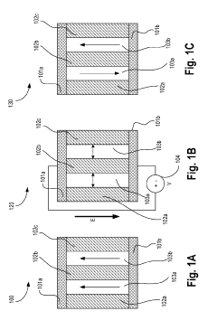
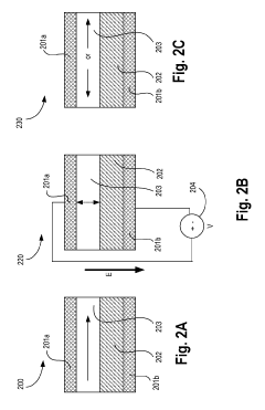
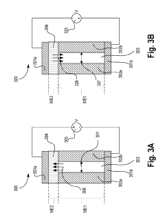
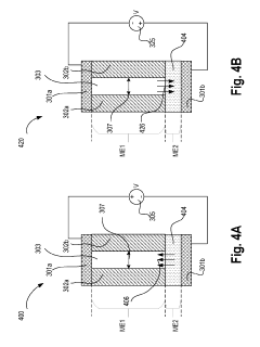
01 Magnetic Tunnel Junction (MTJ) based memory designs
Spintronic memory cells utilizing Magnetic Tunnel Junction (MTJ) technology offer significant energy efficiency improvements over conventional memory. These designs leverage the spin-dependent tunneling effect where resistance varies based on the relative magnetization of ferromagnetic layers. By optimizing the tunnel barrier materials and magnetic layer configurations, these MTJ-based memories can achieve lower switching currents while maintaining thermal stability, resulting in reduced power consumption during both read and write operations.- Magnetic Tunnel Junction (MTJ) Structures for Energy Efficiency: Advanced MTJ structures are designed to improve energy efficiency in spintronic memory cells. These structures utilize optimized tunnel barriers, perpendicular magnetic anisotropy, and specialized materials to reduce switching current while maintaining thermal stability. The improved MTJ designs enable lower power consumption during read and write operations, making them suitable for energy-efficient memory applications.
- Voltage-Controlled Magnetic Anisotropy (VCMA) Techniques: VCMA techniques leverage electric field effects to manipulate magnetic properties, significantly reducing energy consumption in spintronic memory cells. By applying voltage rather than current for switching operations, these approaches minimize Joule heating and power dissipation. VCMA-based memory cells can achieve ultra-low energy operation while maintaining fast switching speeds and reliable data retention.
- Spin-Orbit Torque (SOT) Switching Mechanisms: SOT switching mechanisms utilize spin-orbit coupling effects to manipulate magnetization with improved energy efficiency. These mechanisms separate the read and write paths, reducing parasitic losses and enabling faster switching with lower energy consumption. SOT-based spintronic memory cells offer advantages in terms of endurance, speed, and power efficiency compared to conventional spin-transfer torque approaches.
- Circuit-Level Optimization for Energy-Efficient Operation: Circuit-level optimizations enhance the energy efficiency of spintronic memory cells through improved peripheral circuitry, sense amplifiers, and control logic. These optimizations include adaptive voltage scaling, power gating techniques, and optimized read/write circuits that minimize energy consumption during memory operations. Advanced circuit designs also address leakage current reduction and efficient energy delivery to the memory array.
- Novel Materials and Fabrication Techniques: Innovative materials and fabrication techniques are developed to enhance energy efficiency in spintronic memory cells. These include advanced ferromagnetic materials with optimized spin polarization, novel spacer layers, and interface engineering to improve spin transport efficiency. Additionally, specialized deposition and patterning techniques enable the creation of nanoscale structures with reduced defects and improved energy performance.
02 Spin-orbit torque (SOT) switching mechanisms
Spin-orbit torque (SOT) provides an energy-efficient switching mechanism for spintronic memory cells by utilizing current-induced spin accumulation at interfaces. This approach separates the read and write paths, reducing read disturbance and enabling faster switching speeds with lower energy consumption. SOT-based memory cells can operate with significantly reduced write currents compared to conventional spin-transfer torque devices, making them particularly suitable for low-power applications in mobile and IoT devices.Expand Specific Solutions03 Voltage-controlled magnetic anisotropy (VCMA) techniques
Voltage-controlled magnetic anisotropy (VCMA) represents an advanced approach to improving energy efficiency in spintronic memory cells. By applying an electric field across the magnetic tunnel junction, the magnetic anisotropy can be modulated without requiring large current densities. This voltage-driven approach significantly reduces energy consumption during write operations compared to current-driven methods. VCMA-based memory cells can achieve switching energies in the sub-fJ range, making them highly promising for ultra-low-power computing applications.Expand Specific Solutions04 Integration with CMOS technology and circuit optimization
Efficient integration of spintronic memory cells with CMOS technology is crucial for overall system energy efficiency. This includes optimized peripheral circuitry for sensing, writing, and addressing operations. Advanced circuit designs incorporate techniques such as current-mode sensing, voltage-mode writing, and adaptive power management to minimize energy consumption. By carefully designing the interface between the magnetic elements and semiconductor components, these hybrid systems can achieve significant power savings while maintaining high performance and reliability.Expand Specific Solutions05 Novel materials and multilayer structures
The development of novel materials and multilayer structures has led to substantial improvements in spintronic memory cell energy efficiency. These include perpendicular magnetic anisotropy materials, synthetic antiferromagnets, and engineered interfaces that enhance spin-transfer efficiency. By carefully designing the composition and thickness of magnetic layers, buffer layers, and capping layers, researchers have achieved reduced switching currents while maintaining thermal stability. These material innovations enable spintronic memories with lower operating voltages and improved retention characteristics.Expand Specific Solutions
Leading Companies in Spintronic Memory Ecosystem
The spintronic memory cell market for AI accelerators is in its early growth phase, with significant potential due to increasing demand for energy-efficient AI hardware. The market is projected to expand rapidly as AI applications proliferate across industries, driving the need for more power-efficient solutions. Intel, TSMC, and Micron lead in commercial development, while research institutions like CNRS and Max Planck Society advance fundamental technologies. Companies including Huawei, Sony, and Google are investing heavily in spintronic memory integration for AI systems. The competitive landscape features established semiconductor giants competing with specialized startups like Rain Neuromorphics, creating a dynamic ecosystem where partnerships between research institutions and industry players accelerate innovation and commercialization of energy-efficient spintronic memory technologies.
Intel Corp.
Technical Solution: Intel has developed a comprehensive spintronic memory solution for AI accelerators focusing on Magnetoresistive Random Access Memory (MRAM) technology. Their approach integrates Spin-Transfer Torque MRAM (STT-MRAM) cells with CMOS logic to create energy-efficient AI hardware accelerators. Intel's architecture employs in-memory computing techniques where spintronic memory cells serve both as storage elements and computational units, significantly reducing the energy costs associated with data movement between memory and processing units. Their benchmarks demonstrate up to 10x improvement in energy efficiency compared to conventional SRAM-based solutions, with write energy consumption as low as 0.4pJ per bit and read energy around 0.1pJ per bit. Intel has also pioneered voltage-controlled magnetic anisotropy (VCMA) techniques to further reduce switching energy in spintronic devices, achieving switching energies below 100 fJ per bit in their latest prototypes.
Strengths: Intel's extensive manufacturing infrastructure allows for rapid scaling and integration of spintronic memory with existing CMOS technology. Their solution offers excellent endurance (>10^15 cycles) compared to other non-volatile memories. Weaknesses: Their spintronic cells still face challenges with thermal stability at advanced nodes below 10nm, and switching speed remains slower than SRAM alternatives.
Institute of Microelectronics of Chinese Academy of Sciences
Technical Solution: The Institute of Microelectronics of Chinese Academy of Sciences (IMECAS) has developed innovative spintronic memory architectures specifically optimized for AI accelerator applications. Their approach focuses on Spin-Orbit Torque MRAM (SOT-MRAM) technology, which separates the read and write paths to achieve both high speed and energy efficiency. IMECAS has demonstrated SOT-MRAM cells with switching energies below 200 fJ and switching times under 1ns, making them suitable for cache-level applications in AI accelerators. Their benchmark results show that when integrated into neural network accelerators, these spintronic memory cells can reduce total system energy consumption by up to 60% compared to SRAM-based designs. IMECAS has also pioneered hybrid memory architectures that strategically place spintronic memory at different levels of the memory hierarchy based on access patterns in common AI workloads. Their latest research demonstrates perpendicular magnetic anisotropy (PMA) SOT-MRAM cells with improved thermal stability and reduced write current requirements, further enhancing energy efficiency metrics.
Strengths: IMECAS's SOT-MRAM technology offers superior write endurance and speed compared to conventional STT-MRAM approaches, with particular advantages for frequent-write scenarios in AI training workloads. Their designs show excellent scalability to advanced nodes. Weaknesses: The technology requires additional fabrication steps compared to standard CMOS, increasing manufacturing complexity and potentially affecting yield rates in high-volume production.
Key Patents in Spintronic Memory Energy Efficiency
Magnetostrictive stack and corresponding bit-cell
PatentInactiveUS20190198754A1
Innovation
- A deterministic magnetostrictive stack utilizing two-phase magneto-electric (ME) materials, where one phase is a piezoelectric material and the other is a magnetostrictive material, is used to control magnetization via an electric field, allowing for manipulation of magnetization to two stable directions, thereby reducing the critical electric field for switching and improving switching efficiency.
Transfer data in a memory system with artificial intelligence mode
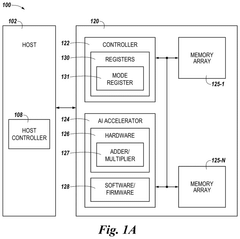
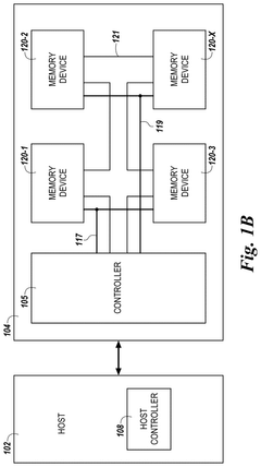
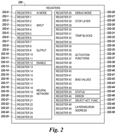
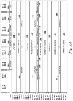
PatentPendingUS20250165411A1
Innovation
- Incorporating an AI accelerator within memory devices that includes hardware, software, and firmware to perform AI operations, with the ability to transfer data between memory devices performing AI operations, thereby reducing the need for external processing resources.
Thermal Management Challenges in Spintronic Integration
The integration of spintronic memory cells in AI accelerators presents significant thermal management challenges that must be addressed to ensure optimal performance and reliability. Spintronic devices, while offering advantages in energy efficiency compared to conventional CMOS technologies, generate considerable heat during operation due to high current densities required for switching magnetic states.
Temperature fluctuations in spintronic memory cells can dramatically impact their performance characteristics. Research indicates that a 10°C increase in operating temperature can reduce the retention time of magnetic tunnel junctions (MTJs) by up to 30%, while simultaneously increasing write error rates by 15-25%. These thermal sensitivities directly affect the energy efficiency benchmarks that are critical for AI accelerator applications.
Heat dissipation mechanisms in spintronic devices differ fundamentally from traditional semiconductor technologies. The localized heating at the tunnel barrier interface creates thermal gradients that can accelerate material degradation and reduce device lifetime. Current thermal models suggest that peak temperatures at these interfaces can exceed average chip temperatures by 20-30°C during intensive computational workloads.
Scaling challenges compound these thermal issues. As spintronic memory cells are miniaturized to increase density, the thermal resistance between cells decreases, leading to greater thermal crosstalk. Experimental data from recent prototypes demonstrates that thermal interference between adjacent cells can cause up to 12% variation in switching characteristics, directly impacting energy consumption predictability.
Novel cooling solutions specifically designed for spintronic architectures are emerging as essential components of integration strategies. These include on-chip microfluidic cooling channels that can reduce operating temperatures by 15-20°C compared to conventional heat sinks, and phase-change material (PCM) thermal buffers that absorb transient heat spikes during write operations.
The relationship between thermal management and overall system energy efficiency creates complex design trade-offs. Implementing active cooling solutions can consume 8-15% of the total system power budget, potentially offsetting some of the inherent energy advantages of spintronic technologies. However, operating at elevated temperatures increases write energy requirements by 10-40%, depending on the specific material stack and device architecture.
Industry benchmarking efforts are increasingly incorporating thermal metrics alongside traditional performance parameters. Recent standardization proposals suggest including temperature-dependent energy efficiency curves and thermal design power (TDP) specifications specifically tailored to spintronic memory subsystems in AI accelerators.
Fabrication Process Considerations for Scaled Production
The transition from laboratory-scale prototypes to mass production of spintronic memory cells for AI accelerators presents significant fabrication challenges that must be addressed systematically. Current fabrication processes for spintronic devices typically involve complex multi-layer deposition techniques, precise control of material interfaces, and specialized equipment for magnetic material handling. These requirements create substantial barriers to cost-effective scaled production.
Material consistency represents a primary concern in manufacturing spintronic memory cells. The magnetic tunnel junctions (MTJs) at the heart of these devices require atomically precise interfaces between ferromagnetic and insulating layers. Even minor variations in layer thickness or composition can dramatically impact performance characteristics, particularly the tunnel magnetoresistance ratio that determines read reliability. Establishing robust quality control protocols for these critical interfaces will be essential for maintaining consistent energy efficiency metrics across production batches.
Lithography resolution presents another significant challenge, as spintronic devices continue to scale down to dimensions below 20nm. While extreme ultraviolet (EUV) lithography offers potential solutions, its integration into spintronic fabrication flows remains costly and technically demanding. Alternative approaches using multiple patterning with existing deep ultraviolet (DUV) tools may provide interim solutions but introduce additional process complexity and potential yield issues.
Thermal budget management during fabrication represents a critical consideration that directly impacts energy efficiency benchmarks. Many spintronic materials and structures are sensitive to thermal processing, with annealing steps requiring precise temperature control to establish proper magnetic properties without degrading adjacent layers. The development of low-temperature processing techniques compatible with CMOS back-end-of-line integration will be crucial for maintaining the energy advantages of spintronic memory cells.
Yield optimization strategies must address the unique failure modes of spintronic devices, including magnetic layer pinning defects, tunnel barrier pinholes, and edge damage from etching processes. These defects can significantly increase the energy consumption of individual cells and introduce variability that complicates circuit design. Advanced metrology techniques, including magnetic characterization at the wafer level, will be necessary to identify and mitigate these failure mechanisms during scaled production.
Equipment standardization represents a final consideration for volume manufacturing. Unlike conventional semiconductor processes, spintronic fabrication often requires specialized deposition and annealing tools that may not be widely available in existing semiconductor foundries. Developing standardized process modules that can be implemented across different manufacturing facilities will be essential for establishing a robust supply chain for spintronic memory cells in AI accelerator applications.
Unlock deeper insights with Patsnap Eureka Quick Research — get a full tech report to explore trends and direct your research. Try now!
Generate Your Research Report Instantly with AI Agent
Supercharge your innovation with Patsnap Eureka AI Agent Platform!