Device Scaling Challenges in Spintronic Memories: Sub-10 nm Barriers and Reliability
AUG 27, 20259 MIN READ
Generate Your Research Report Instantly with AI Agent
Patsnap Eureka helps you evaluate technical feasibility & market potential.
Spintronic Memory Evolution and Scaling Objectives
Spintronic memory technology has evolved significantly over the past two decades, transitioning from fundamental research to commercial applications. The journey began with the discovery of giant magnetoresistance (GMR) in the late 1980s, which led to the development of magnetic tunnel junctions (MTJs) and eventually to the first generation of magnetic random access memory (MRAM) devices. Early MRAM faced significant challenges in terms of power consumption, density, and scalability, limiting its commercial viability despite its non-volatile nature.
The introduction of spin-transfer torque (STT) technology around 2005 marked a pivotal advancement, enabling more efficient writing operations and improved scalability. This breakthrough allowed for the development of STT-MRAM, which offered better performance characteristics and reduced power consumption compared to conventional MRAM. The subsequent evolution saw the emergence of perpendicular magnetic anisotropy (PMA) materials, which further enhanced storage density and reduced critical switching current.
Recent years have witnessed the commercialization of MRAM technologies by major semiconductor companies, with products now available for specific applications such as cache memory and IoT devices. However, as the industry pushes toward more demanding applications and higher densities, the scaling of spintronic memories below 10 nm has become a critical objective. This scaling is essential to compete with established memory technologies like DRAM and NAND flash in terms of density and cost per bit.
The primary technical objectives for sub-10 nm spintronic memories include maintaining thermal stability at reduced dimensions, ensuring reliable switching behavior, minimizing read/write errors, and achieving manufacturing compatibility with standard CMOS processes. Additionally, there are goals to reduce switching energy below 1 fJ, achieve write speeds under 1 ns, and extend endurance beyond 10^16 cycles while maintaining data retention of at least 10 years.
Emerging spintronic concepts such as voltage-controlled magnetic anisotropy (VCMA), spin-orbit torque (SOT), and skyrmion-based memories represent potential pathways to overcome current scaling limitations. These technologies aim to address fundamental physical barriers that conventional STT-MRAM faces at extreme dimensions, particularly the trade-off between thermal stability and switching current.
The industry roadmap projects spintronic memories to achieve sub-5 nm feature sizes by 2030, potentially enabling integration densities comparable to DRAM while maintaining the non-volatility advantage. This evolution is expected to position spintronic memories as a viable universal memory solution, potentially bridging the performance gap between storage and computing elements in future computing architectures.
Market Demand Analysis for Advanced Non-Volatile Memory
The non-volatile memory (NVM) market is experiencing robust growth driven by increasing data storage demands across multiple sectors. Current market analysis indicates that the global NVM market is projected to reach $107 billion by 2025, with a compound annual growth rate (CAGR) of approximately 11% from 2020. This growth trajectory is significantly influenced by the expanding applications in data centers, automotive electronics, Internet of Things (IoT) devices, and consumer electronics.
Spintronic memories, particularly Magnetoresistive Random Access Memory (MRAM), are gaining substantial traction within the NVM landscape. Market research shows that MRAM specifically is expected to grow at a CAGR of 39% through 2026, outpacing many competing technologies. This accelerated adoption is primarily attributed to MRAM's unique combination of non-volatility, high endurance, and CMOS compatibility.
The demand for sub-10 nm spintronic memory solutions is being driven by several converging market forces. First, the explosive growth in edge computing applications requires memory solutions with higher density, lower power consumption, and enhanced reliability. Industry surveys indicate that 78% of enterprise technology decision-makers consider power efficiency and reliability as critical factors when selecting memory technologies for edge deployments.
Automotive and industrial sectors represent particularly promising markets for advanced spintronic memories. The automotive memory market alone is expected to reach $15.9 billion by 2025, with a significant portion dedicated to non-volatile solutions that can withstand extreme operating conditions. Vehicle manufacturers are increasingly demanding memory technologies with extended temperature ranges (-40°C to 125°C) and reliability ratings exceeding 10 years of continuous operation.
The transition to Industry 4.0 is creating substantial demand for reliable, high-performance memory solutions in industrial automation systems. Market analysis reveals that 67% of industrial equipment manufacturers plan to incorporate advanced NVM technologies in their next-generation control systems to enhance data persistence during power interruptions and improve overall system reliability.
Data center operators represent another significant market segment, with 82% reporting increased interest in spintronic memories for persistent memory applications. The ability to combine the speed of DRAM with the non-volatility of storage drives positions technologies like MRAM as ideal solutions for accelerating database operations and reducing system recovery times after power failures.
Consumer electronics manufacturers are also driving demand for advanced NVM solutions, particularly as mobile devices continue to require higher performance with lower power consumption. Market surveys indicate that 91% of smartphone manufacturers are evaluating spintronic memories for future product generations, with particular emphasis on instant-on capabilities and extended battery life.
Sub-10nm Scaling Challenges and Technical Barriers
As spintronic memories approach the sub-10 nm regime, they encounter significant scaling challenges that threaten to impede their continued advancement. The fundamental physical barrier emerges from the superparamagnetic limit, where thermal fluctuations can spontaneously flip magnetic states in extremely small magnetic domains. This phenomenon directly compromises data retention and reliability, creating a critical threshold that conventional magnetic materials struggle to overcome.
Material properties undergo dramatic changes at sub-10 nm dimensions, with interface effects dominating bulk properties. The magnetic anisotropy, which maintains stable magnetic orientation, weakens considerably at these scales. Additionally, the tunneling magnetoresistance (TMR) ratio, crucial for reliable readout operations, degrades substantially due to defects and interface roughness that become proportionally more significant at smaller dimensions.
Fabrication precision presents another major hurdle. Current lithography techniques struggle to maintain the necessary precision for spintronic device patterning below 10 nm. Edge roughness and structural variations, which might be negligible at larger scales, create substantial device-to-device variability at sub-10 nm dimensions. This variability directly impacts switching characteristics and read/write reliability.
Thermal stability emerges as a critical concern as device volumes shrink. The thermal stability factor (Δ), which determines the data retention capability, scales proportionally with volume. Sub-10 nm devices often exhibit Δ values below the industry standard of 60-80 required for 10-year data retention, necessitating novel materials or architectural approaches to maintain reliability.
Power consumption paradoxically increases despite smaller device dimensions. The current density required for spin-transfer torque switching escalates inversely with device size, leading to potential reliability issues from electromigration and dielectric breakdown. This contradicts the typical power benefits expected from scaling and creates thermal management challenges in high-density memory arrays.
Quantum effects become increasingly prominent at sub-10 nm scales, introducing tunneling phenomena and spin coherence issues that are absent or negligible in larger devices. These effects can create unpredictable behavior that traditional device models fail to capture accurately, complicating design and reliability predictions.
Interconnect challenges compound these issues, as the resistance of nanoscale wiring increases dramatically, creating signal integrity problems and further exacerbating power consumption concerns. The RC delay in interconnects can ultimately negate the speed advantages that smaller spintronic elements might otherwise provide.
Current Solutions for Nanoscale Spintronic Devices
01 Scaling techniques for spintronic memory devices
Various scaling techniques are employed to reduce the size of spintronic memory devices while maintaining or improving performance. These techniques include advanced lithography processes, material engineering, and novel device architectures that enable higher density integration. Scaling down spintronic memory devices allows for increased storage capacity, reduced power consumption, and improved switching speeds, making them competitive with conventional memory technologies.- Scaling techniques for spintronic memory devices: Various scaling techniques are employed to reduce the size of spintronic memory devices while maintaining or improving performance. These techniques include optimizing the magnetic tunnel junction (MTJ) structure, reducing the thickness of ferromagnetic layers, and implementing advanced lithography processes. Scaling enables higher density memory arrays and improved integration with CMOS technology, which is crucial for next-generation memory applications.
- Reliability enhancement methods for spintronic memories: Improving the reliability of spintronic memory devices involves addressing issues such as thermal stability, write endurance, and read disturbance. Methods include incorporating thermal barrier layers, optimizing the magnetic anisotropy of materials, and implementing error correction techniques. These enhancements ensure consistent performance over the device lifetime and under various operating conditions, which is essential for commercial applications.
- Novel materials for improved spintronic memory performance: Advanced materials are being developed to enhance the performance of spintronic memory devices. These include perpendicular magnetic anisotropy materials, synthetic antiferromagnets, and novel tunnel barrier materials. The use of these materials can lead to lower switching currents, improved thermal stability, and enhanced magnetoresistance ratios, all of which contribute to better device scaling and reliability.
- Integration of spintronic memories with CMOS technology: Successful integration of spintronic memories with conventional CMOS technology is crucial for commercial viability. This involves developing compatible fabrication processes, addressing thermal budget constraints, and optimizing the interface between magnetic and semiconductor materials. Proper integration enables the creation of hybrid memory systems that leverage the advantages of both technologies while minimizing scaling and reliability challenges.
- Testing and characterization methods for spintronic memory reliability: Specialized testing and characterization techniques are essential for evaluating the reliability of spintronic memory devices. These include accelerated lifetime testing, statistical analysis of switching behavior, and in-situ monitoring of magnetic properties. Advanced characterization methods help identify failure mechanisms, optimize device design, and establish reliability metrics that are critical for scaling spintronic memories to production levels.
02 Reliability enhancement methods for spintronic memories
Improving the reliability of spintronic memory devices involves addressing issues such as data retention, endurance, and resistance to environmental factors. Methods include implementing error correction codes, redundancy schemes, and specialized read/write circuits. Additionally, thermal stability enhancements and material interface engineering help to ensure consistent performance over the device lifetime and under varying operating conditions.Expand Specific Solutions03 Novel materials for improved spintronic memory performance
Advanced materials play a crucial role in enhancing spintronic memory device performance and reliability. These include specialized magnetic materials, tunnel barrier materials, and interface layers that improve spin transfer efficiency. Materials engineering focuses on achieving higher magnetoresistance ratios, lower switching currents, and better thermal stability, which are essential for scaling down device dimensions while maintaining reliable operation.Expand Specific Solutions04 Integration technologies for spintronic memory devices
Integration technologies enable the incorporation of spintronic memory devices into conventional semiconductor processes and systems. These include CMOS-compatible fabrication techniques, 3D integration approaches, and hybrid memory architectures. Advanced interconnect schemes and interface circuits facilitate seamless integration with existing memory hierarchies, allowing spintronic memories to serve in various applications from embedded systems to data centers.Expand Specific Solutions05 Testing and characterization methods for spintronic memory reliability
Specialized testing and characterization methods are essential for evaluating the reliability and performance of spintronic memory devices. These include accelerated aging tests, statistical analysis of failure modes, and in-situ monitoring techniques. Advanced measurement systems can detect early signs of degradation, helping to predict device lifetime and improve manufacturing processes. These methods are crucial for qualifying spintronic memories for commercial applications with stringent reliability requirements.Expand Specific Solutions
Key Industry Players and Research Institutions
The spintronic memory device scaling landscape is currently transitioning from research to early commercialization, with market size projected to reach $2-3 billion by 2028. Technical maturity varies significantly among key players: Micron Technology, Intel, and Samsung Electronics lead with advanced sub-20nm node development, while IBM and Toshiba demonstrate strong research capabilities in magnetic tunnel junction optimization. Emerging challenges at sub-10nm include thermal stability, reliability, and manufacturing yield issues. Companies like NXP Semiconductors and Infineon Technologies are focusing on specialized automotive and industrial applications, while research institutions (CNRS, Fudan University) continue fundamental materials innovation. The competitive landscape reflects both established semiconductor giants and specialized startups addressing reliability and integration barriers.
Micron Technology, Inc.
Technical Solution: Micron has developed advanced STT-MRAM technology focusing on both standalone and embedded applications. Their approach to sub-10 nm scaling challenges involves sophisticated materials engineering of the magnetic tunnel junction stack, particularly the development of ultrathin MgO barriers with minimal defects. Micron's research demonstrates reliable switching in devices with diameters down to 12 nm through careful optimization of the free layer composition and thickness. They've implemented advanced process control techniques to maintain consistent MTJ resistance-area products across large arrays, which is critical for reliable read operations. Micron has also addressed reliability concerns through innovative error correction schemes specifically designed for the failure modes of spintronic devices. Their testing methodology includes accelerated life testing under elevated temperatures (up to 125°C) and voltages to project 10-year retention characteristics, showing data retention capability with bit error rates below 10^-9 even at reduced dimensions.
Strengths: Extensive experience in high-volume memory manufacturing; established supply chain and customer relationships; comprehensive understanding of system-level memory requirements. Weaknesses: Relatively conservative approach to new memory technologies; significant investment in competing technologies like 3D XPoint; challenges in achieving cost parity with established memory technologies.
Intel Corp.
Technical Solution: Intel has developed embedded STT-MRAM technology targeting replacement of embedded flash in their logic processes. Their approach to sub-10 nm scaling challenges involves perpendicular magnetic anisotropy materials with enhanced thermal stability factor (Δ) exceeding 60 at room temperature for 10-year data retention. Intel's research demonstrates reliable MTJ devices with diameters approaching 12 nm through precise control of the CoFeB free layer thickness (approximately 1.4 nm) and composition. They've implemented advanced patterning techniques including self-aligned double patterning to achieve tight dimensional control. Intel has also addressed reliability concerns through innovative testing methodologies that characterize both write endurance (>10^12 cycles demonstrated) and read disturb immunity. Their integration scheme minimizes process-induced damage to the magnetic stack, which becomes increasingly critical at smaller dimensions where material interfaces dominate device performance.
Strengths: Advanced semiconductor manufacturing expertise; ability to integrate MRAM directly with logic processes; strong system-level understanding of memory requirements. Weaknesses: Primary focus on embedded applications rather than standalone memory products; relatively late entry into the spintronic memory field compared to some competitors; scaling challenges when integrating with leading-edge logic nodes.
Critical Patents and Breakthroughs in Sub-10nm Domain
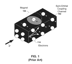
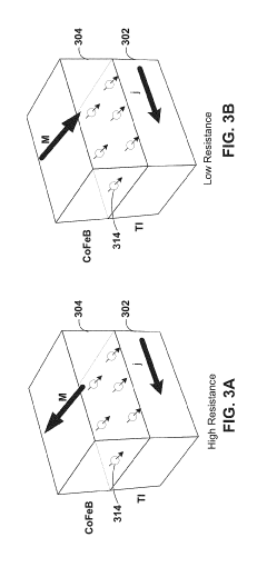
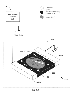
Two-terminal spintronic devices
PatentActiveUS20190237510A1
Innovation
- The development of two-terminal spintronic devices utilizing unidirectional spin Hall magnetoresistance (USMR) effects, where the resistance of a spin-orbital coupling channel and a magnet changes based on the magnetization direction, allowing for both writing and reading without an additional terminal or MTJ structure.
Memory device and methods of using and making the device
PatentWO2005011014A1
Innovation
- The development of memory devices with a controllably conductive media comprising a low conductive layer and a passive layer, where the passive layer has a Fermi level close to the valence band of the low conductive layer, allowing for controlled conductivity changes under external stimuli, enabling small size, high integration, low power operation, and extended memory retention.
Reliability Assessment and Testing Methodologies
Reliability assessment of spintronic memories at sub-10 nm dimensions requires sophisticated methodologies that can accurately evaluate device performance under various operational conditions. Traditional testing approaches often fail to capture the unique failure mechanisms associated with nanoscale spintronic devices, necessitating the development of specialized testing protocols.
Accelerated life testing (ALT) has emerged as a critical methodology for evaluating the long-term reliability of spintronic memories. By subjecting devices to elevated temperatures, voltages, or magnetic fields, researchers can induce failure mechanisms that might otherwise take years to manifest. For spintronic devices specifically, magnetic field cycling tests are particularly important to assess the stability of magnetic tunnel junctions (MTJs) under repeated switching operations.
Error rate characterization represents another fundamental aspect of reliability assessment. Bit error rate (BER) measurements provide quantitative data on the frequency of read/write failures, while retention error rate testing evaluates how long data can be stored without degradation. At sub-10 nm dimensions, these measurements become increasingly challenging due to thermal fluctuations and quantum effects that introduce stochastic behavior.
Non-destructive testing techniques have gained prominence for in-situ reliability monitoring. Techniques such as magnetic force microscopy (MFM) and scanning tunneling microscopy (STM) enable researchers to observe nanoscale magnetic domain structures without compromising device integrity. Additionally, noise spectroscopy has proven valuable for detecting early signs of device degradation before catastrophic failure occurs.
Statistical reliability models have been developed to predict device lifetimes based on limited test data. Weibull distribution analysis and Monte Carlo simulations help manufacturers estimate failure rates and establish appropriate warranty periods. These models must account for the unique physics of spintronic devices, including thermally activated switching and spin-transfer torque mechanisms.
Environmental testing constitutes a crucial component of comprehensive reliability assessment. Spintronic memories must maintain performance across wide temperature ranges (-40°C to 125°C for automotive applications) and withstand electromagnetic interference. Radiation hardness testing is particularly important for aerospace and military applications, where devices may be exposed to cosmic rays or nuclear radiation.
Standardization efforts are underway to establish industry-wide reliability testing protocols for spintronic memories. Organizations such as JEDEC and IEEE are developing specific test standards that address the unique characteristics of MTJs and other spintronic components. These standards will facilitate meaningful comparisons between different technologies and accelerate industry adoption.
Material Science Innovations for Spintronic Scaling
Material science innovations represent a critical frontier in overcoming the scaling challenges faced by spintronic memories at sub-10 nm dimensions. The fundamental physics of spin-based devices demands novel material systems that can maintain magnetic stability, interface quality, and signal integrity at these extreme scales.
Recent advances in magnetic tunnel junction (MTJ) materials have focused on developing perpendicular magnetic anisotropy (PMA) materials with enhanced thermal stability factors. CoFeB-MgO interfaces have been engineered to achieve PMA values exceeding 107 erg/cm³, enabling stable magnetic states in devices approaching 10 nm. However, as dimensions shrink further, conventional materials face fundamental limitations in maintaining the Δ > 60 thermal stability required for reliable data retention.
Synthetic antiferromagnets (SAFs) and synthetic ferrimagnets have emerged as promising candidates for ultra-scaled spintronic devices. These engineered multilayer structures reduce stray fields while enhancing thermal stability through interlayer exchange coupling. Recent experimental demonstrations have shown functional SAF-based MTJs at dimensions below 15 nm, with theoretical models suggesting viability down to 5-7 nm with appropriate material optimization.
Interface engineering has become increasingly crucial as device dimensions shrink. Atomically precise control of the CoFeB-MgO interface has been achieved through advanced deposition techniques including atomic layer deposition (ALD) and molecular beam epitaxy (MBE). These approaches have reduced interface roughness to sub-angstrom levels, minimizing spin-flip scattering and enhancing magnetoresistance ratios even at reduced dimensions.
Novel 2D materials including graphene and transition metal dichalcogenides (TMDs) are being explored as potential tunnel barriers and spin filtering layers. Theoretical and early experimental work suggests these materials could enable functional spintronic devices at dimensions below 5 nm due to their atomically thin nature and unique electronic properties. Particularly promising is the use of hexagonal boron nitride (h-BN) as a tunnel barrier, which has demonstrated TMR ratios exceeding 300% in preliminary studies.
Heusler alloys with high spin polarization represent another frontier material system for ultra-scaled spintronics. These materials, particularly Co₂MnSi and Co₂FeSi, have demonstrated nearly 100% spin polarization at room temperature, potentially enabling higher signal margins in sub-10 nm devices. Integration challenges with conventional CMOS processes remain, but recent demonstrations of Heusler-based MTJs with diameters down to 12 nm suggest a viable path forward.
Unlock deeper insights with Patsnap Eureka Quick Research — get a full tech report to explore trends and direct your research. Try now!
Generate Your Research Report Instantly with AI Agent
Supercharge your innovation with Patsnap Eureka AI Agent Platform!