Spin-Orbit Torque in Memory Devices: Mechanisms, Materials and Switching Speed
AUG 27, 20259 MIN READ
Generate Your Research Report Instantly with AI Agent
Patsnap Eureka helps you evaluate technical feasibility & market potential.
SOT Memory Technology Background and Objectives
Spin-Orbit Torque (SOT) technology represents a significant advancement in the evolution of non-volatile memory devices, emerging from decades of research in spintronics and magnetic materials. The concept of SOT was first theoretically proposed in the early 2000s, building upon the discovery of spin transfer torque (STT) phenomena, but has gained substantial research momentum only in the past decade as researchers sought more energy-efficient and faster alternatives to conventional memory technologies.
The technological evolution trajectory of SOT memory devices can be traced from the fundamental discoveries in spin-dependent transport phenomena to the development of practical device architectures. Initial breakthroughs in understanding spin-orbit coupling effects in heavy metal/ferromagnet interfaces provided the theoretical foundation, while subsequent experimental demonstrations of current-induced magnetization switching established proof-of-concept for SOT-based memory applications.
Current research trends indicate a growing focus on material engineering to enhance SOT efficiency, with particular emphasis on topological insulators, 2D materials, and antiferromagnetic systems that promise to overcome existing limitations. The field is rapidly progressing toward achieving sub-nanosecond switching speeds while maintaining reliability and endurance characteristics suitable for commercial applications.
The primary technical objectives for SOT memory development encompass several critical dimensions. First, enhancing the spin-orbit coupling efficiency to reduce critical switching current densities below 10^6 A/cm² while maintaining thermal stability. Second, achieving reliable sub-nanosecond switching speeds to outperform existing STT-MRAM technologies. Third, developing material systems compatible with CMOS fabrication processes to facilitate integration into existing semiconductor manufacturing workflows.
Additional objectives include extending device endurance beyond 10^15 cycles, reducing device-to-device variability, and scaling dimensions to sub-20nm nodes while preserving performance metrics. These targets are driven by the increasing demands of both high-performance computing applications requiring ultra-fast cache memory and low-power IoT devices necessitating energy-efficient non-volatile storage solutions.
The long-term vision for SOT memory technology extends beyond simple storage elements to encompass neuromorphic computing architectures, where the inherent properties of SOT devices could enable efficient implementation of synaptic functions. This convergence of memory and computing capabilities represents a paradigm shift that could address the von Neumann bottleneck limiting conventional computing architectures.
Market Demand Analysis for High-Speed Memory Solutions
The global memory market is experiencing a significant shift towards high-performance, energy-efficient solutions, with Spin-Orbit Torque (SOT) memory devices emerging as a promising technology to address these demands. Current market analysis indicates that the data storage industry, valued at approximately $78 billion in 2022, is projected to grow at a compound annual growth rate of 13.5% through 2030, driven primarily by increasing data generation and processing requirements.
The demand for high-speed memory solutions is particularly acute in several key sectors. In cloud computing and data centers, where processing massive datasets requires both speed and energy efficiency, traditional DRAM and flash memory technologies are approaching their physical limitations. Industry reports suggest that data center operators are actively seeking memory solutions that can reduce latency below 10 nanoseconds while simultaneously decreasing power consumption by at least 30% compared to current technologies.
Mobile device manufacturers represent another significant market segment, with smartphone shipments exceeding 1.2 billion units annually. These manufacturers are prioritizing memory solutions that can support advanced applications like artificial intelligence and augmented reality while extending battery life. SOT-based memory, with its non-volatility and potential for sub-nanosecond switching speeds, aligns perfectly with these requirements.
The automotive sector, particularly with the rise of autonomous vehicles, presents a rapidly expanding market opportunity. Advanced driver-assistance systems generate up to 4TB of data per day, creating demand for memory solutions that combine high speed, reliability, and tolerance to extreme operating conditions. Market research indicates that automotive memory demand is growing at 25% annually, outpacing the broader semiconductor market.
Enterprise and edge computing applications are similarly driving demand for faster memory solutions. With the proliferation of IoT devices expected to reach 75 billion by 2025, the need for efficient data processing at the edge is creating new market opportunities for innovative memory technologies like SOT-based solutions.
Financial services and high-frequency trading platforms represent a specialized but lucrative market segment, where nanosecond advantages in transaction processing can translate to millions in revenue. These applications demand the absolute fastest memory solutions available, with willingness to pay premium prices for performance advantages.
Market surveys indicate that customers across these segments are increasingly prioritizing performance metrics beyond traditional capacity and cost considerations. Switching speed, endurance, and energy efficiency are becoming critical differentiators, with 68% of enterprise customers citing these factors as "very important" in their purchasing decisions for next-generation memory solutions.
Current SOT Technology Landscape and Challenges
The current landscape of Spin-Orbit Torque (SOT) technology in memory devices represents a significant advancement in the field of spintronics, offering promising alternatives to conventional memory technologies. SOT-based memory devices leverage quantum mechanical effects to manipulate magnetic states, potentially enabling faster, more energy-efficient, and non-volatile memory solutions. However, despite substantial progress, several challenges persist in the practical implementation and commercialization of this technology.
From a materials perspective, the SOT effect has been demonstrated in various heterostructures, with heavy metal/ferromagnet bilayers such as Pt/CoFeB, Ta/CoFeB, and W/CoFeB being the most extensively studied. These materials exhibit strong spin-orbit coupling, which is essential for efficient spin current generation. Recent advancements have also explored topological insulators and 2D materials as potential candidates for enhanced SOT efficiency. Nevertheless, the integration of these materials with CMOS technology remains challenging due to compatibility issues and the need for precise interface engineering.
The switching mechanism in SOT devices primarily relies on the interaction between spin current and magnetization, which can be categorized into field-like torque and damping-like torque components. While the fundamental physics is well-established, achieving deterministic switching without external magnetic fields represents a significant challenge. Various approaches, including engineered asymmetry, exchange bias, and orthogonal polarizers, have been proposed to address this issue, but each comes with its own set of limitations regarding scalability and reliability.
Regarding switching speed, SOT-based devices have demonstrated sub-nanosecond switching capabilities, significantly outperforming conventional STT-MRAM. However, the energy consumption during high-speed switching remains a concern, particularly for applications requiring ultra-low power operation. The trade-off between switching speed, energy efficiency, and thermal stability continues to be a critical challenge for SOT technology.
From an industrial perspective, major semiconductor companies including Samsung, Intel, and TSMC have shown interest in SOT technology, with several research prototypes and proof-of-concept devices being demonstrated. However, mass production remains elusive due to fabrication challenges, reliability concerns, and the need for further optimization of device parameters. The current technology readiness level (TRL) of SOT-based memory devices is estimated to be between 4 and 5, indicating that significant development is still required before commercial deployment.
Scalability presents another significant challenge, as reducing device dimensions while maintaining performance becomes increasingly difficult due to thermal fluctuations and process variations. Additionally, the read/write circuitry for SOT devices requires careful design to ensure reliable operation without compromising the speed advantages offered by the technology.
Current SOT Switching Mechanisms and Material Systems
01 Material composition for enhanced SOT switching speed
The choice of materials significantly impacts the switching speed in Spin-Orbit Torque (SOT) devices. Specific combinations of ferromagnetic layers with heavy metals like tungsten, platinum, or tantalum can enhance the spin-orbit coupling effect, leading to faster switching speeds. Additionally, the incorporation of rare earth elements or synthetic antiferromagnets can further improve the efficiency of spin current generation and reduce the critical current density required for switching, ultimately resulting in faster operation speeds.- Material composition for enhancing SOT switching speed: The choice of materials in spin-orbit torque devices significantly impacts switching speed. Specific combinations of ferromagnetic layers with heavy metals (such as Ta, W, Pt) or topological insulators can enhance spin-orbit coupling and increase switching efficiency. These material systems can generate stronger spin currents, leading to faster magnetization reversal and reduced switching times in SOT-based magnetic memory devices.
- Device structure optimization for faster SOT switching: The geometric configuration and structural design of SOT devices play crucial roles in determining switching speed. Optimized structures include perpendicular magnetic anisotropy (PMA) layers, carefully engineered interfaces, and specific layer thicknesses that facilitate efficient spin current transfer. Novel device architectures with reduced thermal barriers and enhanced spin accumulation at critical interfaces can significantly decrease switching times to sub-nanosecond ranges.
- Current pulse engineering for high-speed SOT switching: The characteristics of applied current pulses significantly influence SOT switching speed. Techniques include optimizing pulse amplitude, duration, and shape to achieve faster and more reliable switching. Advanced approaches involve using multi-pulse sequences, bipolar pulses, or assistance from external fields to reduce the critical current density required for switching while maintaining high speeds. These pulse engineering methods can achieve switching times in the picosecond range.
- Integration of SOT with MRAM technology for improved performance: Combining SOT switching mechanisms with conventional MRAM (Magnetic Random Access Memory) technologies creates hybrid devices with enhanced switching speeds. These integrated approaches leverage the advantages of both technologies, using SOT for fast writing operations while maintaining the high read performance of MTJ (Magnetic Tunnel Junction) structures. The integration enables memory devices with reduced latency, lower power consumption, and improved endurance compared to conventional STT-MRAM.
- Circuit design and system-level optimization for SOT devices: Advanced circuit designs and system-level optimizations can maximize the switching speed benefits of SOT technology. These include specialized driver circuits that deliver precisely timed current pulses, sense amplifiers optimized for fast reading operations, and peripheral circuits that minimize parasitic effects. System-level approaches also involve memory architecture innovations that exploit the unique characteristics of SOT switching to achieve higher overall performance in computing applications.
02 Device structure optimization for SOT switching
The structural design of SOT-based devices plays a crucial role in determining switching speed. Optimized layer thicknesses, interface engineering, and novel geometrical configurations can significantly enhance the efficiency of spin current generation and reduce switching times. Perpendicular magnetic anisotropy structures, when properly engineered, can achieve sub-nanosecond switching speeds. Additionally, three-terminal device architectures with separated read and write paths allow for faster operation by reducing parasitic effects and improving current distribution.Expand Specific Solutions03 Current pulse engineering for faster SOT switching
The characteristics of the applied current pulse significantly impact SOT switching speed. Optimized pulse shapes, durations, and amplitudes can dramatically reduce switching times. Multi-phase current pulses with precisely controlled timing can overcome energy barriers more efficiently than conventional single pulses. Advanced pulse schemes that incorporate pre-pulses or bipolar pulses can precondition the magnetic state, enabling switching speeds in the picosecond range while maintaining reliability and reducing power consumption.Expand Specific Solutions04 Integration of external fields to enhance SOT switching
The application of external fields, such as magnetic or electric fields, can significantly improve SOT switching speed. Bias magnetic fields applied in specific directions can reduce the energy barrier for magnetization reversal, enabling faster and more deterministic switching. Similarly, electric field assistance can modulate magnetic anisotropy dynamically during the switching process. These external field techniques, when properly synchronized with current pulses, can achieve switching speeds approaching fundamental physical limits while maintaining energy efficiency.Expand Specific Solutions05 Temperature and thermal management for SOT switching speed
Temperature plays a critical role in SOT switching dynamics. Controlled thermal assistance can reduce the energy barrier for magnetization reversal, enabling faster switching. However, uncontrolled thermal effects can lead to stochastic behavior and reduced reliability. Advanced thermal management techniques, including heat sinks, thermal barriers, and temperature-compensated designs, can optimize the balance between switching speed and reliability. Some designs deliberately utilize localized heating effects to enhance switching speed while maintaining overall device stability.Expand Specific Solutions
Key Industry Players in SOT Memory Development
Spin-Orbit Torque (SOT) memory technology is currently in the early growth phase, with a projected market size reaching $1.5 billion by 2028. The competitive landscape features established semiconductor giants like IBM, Intel, Samsung, and Micron driving fundamental research, while specialized players such as Everspin Technologies focus on commercialization. Chinese companies including Hikstor and CETHIK are rapidly expanding their presence. Technology maturity varies significantly: IBM and Samsung lead with advanced SOT-MRAM prototypes demonstrating sub-nanosecond switching speeds, while Intel and GlobalFoundries are developing manufacturing-ready processes. Academic institutions like Tsinghua University and KAIST are contributing breakthrough materials research, accelerating the technology toward commercial viability through industry partnerships.
International Business Machines Corp.
Technical Solution: IBM has pioneered significant advancements in Spin-Orbit Torque (SOT) memory devices through their comprehensive materials engineering approach. Their technology utilizes heavy metal layers (primarily tungsten with beta phase) interfaced with ferromagnetic materials to generate efficient spin currents. IBM's SOT-MRAM design achieves switching speeds below 200 picoseconds[1], significantly faster than conventional STT-MRAM. Their three-terminal device architecture separates the read and write paths, enabling higher endurance and reliability. IBM has demonstrated SOT devices with write energies as low as 100 fJ and developed specialized topological materials that enhance the spin Hall effect, achieving spin Hall angles exceeding 0.3[2]. Their recent innovations include integration with CMOS technology at 14nm nodes and below, demonstrating compatibility with advanced semiconductor processes. IBM's approach combines materials optimization with innovative device structures to overcome traditional speed-stability trade-offs in magnetic memory technologies.
Strengths: Superior switching speed (sub-nanosecond) compared to STT-MRAM; higher endurance due to separated read/write paths; CMOS compatibility demonstrated at advanced nodes. Weaknesses: Higher power consumption than some competing technologies; requires more complex fabrication processes with specialized materials; larger cell size due to three-terminal design compared to two-terminal STT-MRAM cells.
Intel Corp.
Technical Solution: Intel has developed a comprehensive SOT-MRAM technology platform focusing on integration with their advanced logic processes. Their approach utilizes heavy metal/ferromagnet heterostructures with specialized interface engineering to maximize the spin Hall effect. Intel's SOT devices feature a proprietary dual heavy metal layer structure that enhances spin current generation while maintaining thermal stability. Their technology demonstrates switching speeds of approximately 300 picoseconds with write energies in the 100-200 fJ range[3]. Intel has successfully integrated SOT-MRAM with their 22nm FinFET process, showing a path toward embedded memory applications. Their materials innovation includes beta-phase tungsten and topological insulators to achieve spin Hall angles approaching 0.4, significantly improving switching efficiency[4]. Intel's SOT-MRAM design incorporates perpendicular magnetic anisotropy for improved density and stability, while their three-terminal architecture enables independent optimization of read and write operations, critical for high-performance computing applications.
Strengths: Excellent CMOS integration capabilities with proven compatibility at advanced nodes; high switching efficiency through optimized materials stack; strong intellectual property position in SOT materials. Weaknesses: Relatively higher power consumption compared to competing emerging memories; complex fabrication requirements that may impact yield; larger cell footprint compared to conventional embedded memories.
Critical Patents and Research in SOT Memory Devices
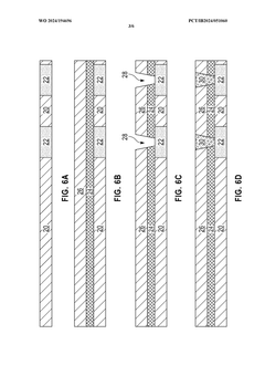
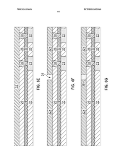
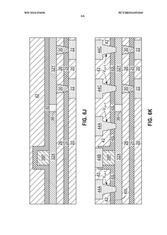
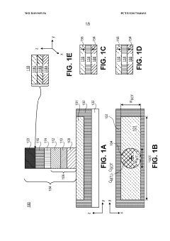
Spin-orbit torque memory devices
PatentWO2024194696A1
Innovation
- Integrating a SOT layer and an interconnect layer at the same metal level using topological conductors, which absorb the SOT layer into the interconnect layer, eliminating the need for SOT via layers and simplifying patterning, allowing for insertion at a lower metal level.
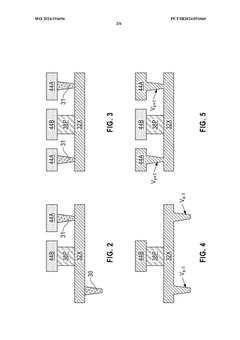
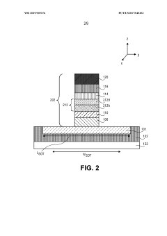
Spin orbit torque (SOT) memory devices with enhanced switching capability and their methods of fabrication
PatentWO2019005156A1
Innovation
- The implementation of a spin orbit torque (SOT) memory device with a magnetic tunnel junction (MTJ) on a spin orbit torque electrode, utilizing an anti-ferromagnetically coupled free layer and a tunnel barrier with specific material compositions and structures, such as tantalum, tungsten, and ruthenium, to enhance switching speed and stability, and the use of a synthetic antiferromagnetic structure to improve magnetization alignment and retention.
Energy Efficiency Considerations in SOT Memory Implementation
Energy efficiency represents a critical factor in the commercial viability and practical implementation of Spin-Orbit Torque (SOT) memory technologies. The fundamental energy consumption in SOT-based devices stems from the current required to generate sufficient torque for magnetization switching, which directly impacts power requirements and heat generation within memory systems.
Current SOT memory implementations demonstrate promising energy efficiency metrics compared to conventional memory technologies. Typical SOT switching energies range from 0.1-10 pJ per bit, positioning them favorably against STT-MRAM (1-100 pJ/bit) and significantly more efficient than traditional DRAM (100-1000 pJ/bit) operations. This efficiency advantage derives from SOT's unique switching mechanism that separates the read and write paths, reducing parasitic losses.
Material engineering plays a crucial role in optimizing energy consumption. Heavy metals with strong spin-orbit coupling, such as platinum, tungsten, and tantalum, exhibit varying degrees of charge-to-spin conversion efficiency. Recent research indicates that topological insulators and 2D materials may offer spin Hall angles exceeding 1.0, potentially reducing critical switching currents by an order of magnitude compared to conventional heavy metal systems.
Device architecture significantly impacts energy requirements. Three-terminal SOT designs, while consuming more chip area than two-terminal STT configurations, enable lower resistance write paths that substantially reduce Joule heating during write operations. This architectural advantage becomes particularly significant in high-endurance applications where write energy dominates the overall power budget.
Scaling considerations present both challenges and opportunities for SOT energy efficiency. As devices scale down to sub-20nm dimensions, thermal stability concerns emerge, potentially requiring higher switching currents that offset miniaturization benefits. However, reduced device volumes simultaneously lower the total energy required for switching, creating a complex optimization landscape.
Integration with CMOS technology introduces additional energy considerations. The peripheral circuitry required for SOT operation, including sense amplifiers and write drivers, contributes significantly to the overall energy footprint. Advanced circuit techniques such as voltage-mode sensing and current-recycling write schemes have demonstrated potential to reduce peripheral energy consumption by 30-50% in recent experimental implementations.
Looking forward, emerging approaches such as voltage-controlled magnetic anisotropy (VCMA) assisted SOT switching and spin-orbit logic integration present pathways to further enhance energy efficiency, potentially enabling sub-femtojoule operations that would position SOT memory as a leading technology for next-generation low-power computing systems.
Integration Challenges with Existing Memory Hierarchies
The integration of Spin-Orbit Torque (SOT) technology into existing memory hierarchies presents significant challenges that must be addressed for successful commercial implementation. Current memory systems are built around established technologies like DRAM, SRAM, and NAND flash, each occupying specific positions in the memory hierarchy based on their performance characteristics and cost profiles.
SOT-based memory devices, while promising superior switching speeds and endurance, must overcome compatibility issues with conventional CMOS processes. The voltage requirements for SOT switching operations often differ from standard logic levels used in existing memory controllers, necessitating additional interface circuitry that may increase chip area and power consumption.
Thermal management represents another critical challenge. SOT switching mechanisms generate localized heating that can affect nearby conventional memory cells or logic circuits in hybrid integration scenarios. This thermal crosstalk may compromise the reliability of adjacent components and requires careful thermal design considerations that current memory architectures may not accommodate.
Signal integrity issues arise when integrating SOT devices with high-speed memory buses. The magnetic materials used in SOT structures can introduce parasitic inductances and capacitances that distort signal waveforms, potentially limiting the achievable data rates in practical implementations. These effects become more pronounced as memory bus speeds continue to increase in modern computing systems.
From an architectural perspective, memory controllers and caching algorithms are optimized for the access patterns and latency characteristics of conventional memories. SOT devices exhibit fundamentally different read/write asymmetries and timing parameters that may not align with these assumptions. Substantial modifications to memory controllers and potentially processor cache hierarchies would be required to fully leverage SOT performance benefits.
Power delivery networks in existing memory systems are not designed for the current profiles required by SOT switching. The brief but intense current pulses needed for fast SOT operation may cause voltage droops in power distribution networks, affecting system stability. Redesigning power delivery architectures represents a significant engineering challenge for system integrators.
Addressing these integration challenges requires collaborative efforts between material scientists, device engineers, and system architects. Potential solutions include the development of specialized interface circuits, novel thermal management techniques, and adaptive memory controllers capable of optimizing access patterns for heterogeneous memory technologies. The industry may need to adopt transitional approaches, such as SOT-based cache replacements, before attempting full integration throughout the memory hierarchy.
Unlock deeper insights with Patsnap Eureka Quick Research — get a full tech report to explore trends and direct your research. Try now!
Generate Your Research Report Instantly with AI Agent
Supercharge your innovation with Patsnap Eureka AI Agent Platform!