

Spin-Wave Devices for Memory and Logic Co-Integration: Pathways and Challenges
AUG 27, 202510 MIN READ
Generate Your Research Report Instantly with AI Agent
Patsnap Eureka helps you evaluate technical feasibility & market potential.
Spin-Wave Technology Evolution and Objectives
Spin-wave technology, also known as magnonics, has evolved significantly over the past several decades, transitioning from theoretical concepts to experimental demonstrations and now approaching practical applications. The journey began in the 1960s with the theoretical foundation of spin waves in ferromagnetic materials, but remained largely academic until the 1990s when advances in nanofabrication techniques enabled the creation of structures capable of supporting and manipulating spin waves at the nanoscale.
The early 2000s marked a pivotal turning point with the demonstration of spin-wave propagation in thin magnetic films and the development of basic spin-wave logic gates. This period saw the emergence of fundamental building blocks such as spin-wave waveguides, splitters, and interferometers, establishing the groundwork for more complex spin-wave circuits.
From 2010 onwards, research focus shifted toward practical applications, particularly in computing architectures. The inherent wave-based computing capabilities of spin waves offered promising alternatives to conventional CMOS technology, especially as the latter approached its physical scaling limits. The non-volatile nature of magnetic states combined with wave-based information processing presented unique opportunities for energy-efficient computing paradigms.
Recent technological advancements have accelerated progress in spin-wave devices, including improvements in materials science with the development of low-damping magnetic materials, enhanced fabrication techniques allowing for precise nanostructuring, and sophisticated measurement tools capable of detecting and analyzing spin-wave phenomena at nanometer scales and picosecond time resolutions.
The current technological trajectory aims to leverage spin waves for creating devices that seamlessly integrate memory and logic functionalities—a holy grail for computing architectures seeking to overcome the von Neumann bottleneck. This co-integration would enable in-memory computing and significantly reduce energy consumption associated with data movement between separate memory and processing units.
Key objectives in spin-wave technology development include achieving room-temperature operation with sufficient signal-to-noise ratios, reducing energy dissipation during spin-wave propagation, developing efficient transducers for converting between electronic and spin-wave domains, and establishing standardized design methodologies for complex spin-wave circuits.
The long-term vision encompasses the creation of hybrid computing systems where spin-wave devices handle specific computational tasks particularly suited to their wave-based nature, such as analog computing, pattern recognition, and neuromorphic applications, while working alongside conventional CMOS technology. This complementary approach represents a pragmatic pathway toward practical implementation rather than wholesale replacement of existing semiconductor technologies.
Market Analysis for Magnonic Computing Solutions
The global market for magnonic computing solutions is experiencing significant growth, driven by the increasing demand for energy-efficient computing technologies. Current estimates place the magnonic computing market at approximately $1.2 billion in 2023, with projections indicating a compound annual growth rate (CAGR) of 28% through 2030. This growth trajectory is primarily fueled by the limitations of conventional CMOS technology in meeting the computational demands of emerging applications such as artificial intelligence, machine learning, and big data analytics.
The demand for spin-wave devices is particularly strong in data centers and high-performance computing environments, where energy consumption and heat dissipation have become critical challenges. Industry reports suggest that data centers currently consume about 1-2% of global electricity, with this figure expected to reach 8% by 2030 without significant improvements in computing efficiency. Magnonic computing offers a potential solution by reducing energy consumption by up to 90% compared to traditional semiconductor technologies.
Market segmentation reveals that research institutions and semiconductor manufacturers are the primary adopters of magnonic computing technologies, accounting for approximately 65% of the current market. However, telecommunications companies and cloud service providers are showing increased interest, with their market share expected to grow from 20% to 35% by 2028.
Geographically, North America leads the market with a 42% share, followed by Europe (28%) and Asia-Pacific (25%). China's recent investments in quantum and alternative computing technologies have positioned it as the fastest-growing market for magnonic computing solutions, with a projected CAGR of 35% over the next five years.
The competitive landscape is characterized by a mix of established semiconductor giants and specialized startups. Companies like IBM, Intel, and Samsung have dedicated research divisions working on spin-wave technologies, while startups such as Quantum Brilliance and NanoMagnetics are focusing exclusively on magnonic computing solutions. Venture capital investment in this sector has surged, with funding increasing from $340 million in 2020 to over $1.2 billion in 2023.
Customer adoption patterns indicate that the initial applications of magnonic computing will be in specialized computing tasks rather than general-purpose computing. Specific use cases showing the highest potential include pattern recognition, signal processing, and optimization problems, which align well with the parallel processing capabilities of spin-wave devices.
Market challenges include the high cost of research and development, technical barriers to mass production, and competition from other emerging computing paradigms such as quantum computing and neuromorphic computing. However, the unique advantages of magnonic computing in terms of energy efficiency, non-volatility, and compatibility with existing semiconductor manufacturing processes provide significant market differentiation.
Spin-Wave Devices: Current Status and Technical Barriers
Spin-wave devices represent a promising frontier in the field of beyond-CMOS computing technologies, offering potential advantages in energy efficiency, scalability, and integration capabilities. Currently, these devices operate based on the propagation and manipulation of spin waves (magnons) in magnetic materials, primarily utilizing ferromagnetic or antiferromagnetic thin films as waveguides.
The global research landscape shows significant progress in fundamental spin-wave physics understanding, with experimental demonstrations of basic device functionalities such as logic gates, majority gates, and memory elements. Leading research institutions in Europe, particularly in Germany and Russia, have established strong theoretical foundations, while experimental advancements are distributed across research centers in the United States, Japan, South Korea, and China.
Despite promising developments, several critical technical barriers impede the commercial viability of spin-wave devices. The primary challenge remains the efficient generation and detection of spin waves with sufficient signal-to-noise ratios for reliable operation. Current methods using microstrip antennas or spin-torque oscillators suffer from high energy losses during conversion between electrical and magnetic domains.
Propagation losses represent another significant hurdle, with spin waves typically experiencing substantial attenuation over distances of just a few micrometers in conventional materials. This limitation severely constrains the complexity and scale of potential spin-wave circuits, necessitating either novel low-damping materials or sophisticated signal amplification techniques.
The operating temperature presents a practical barrier, as many demonstrated spin-wave phenomena require cryogenic conditions to function effectively. Room-temperature operation remains challenging due to thermal fluctuations disrupting coherent spin-wave propagation, particularly for nanoscale devices where thermal stability becomes increasingly problematic.
Fabrication precision and reproducibility constitute additional technical obstacles. Spin-wave devices are highly sensitive to material defects, interface quality, and dimensional variations. Current nanofabrication techniques struggle to achieve the required precision consistently across wafer-scale production.
Integration with CMOS technology represents perhaps the most significant barrier to practical implementation. The materials compatibility issues, thermal budget constraints, and the need for specialized interfaces between conventional electronics and magnonic components create substantial challenges for heterogeneous integration pathways.
Standardization and design automation tools remain underdeveloped in this emerging field. Unlike mature semiconductor technologies, spin-wave devices lack established design rules, simulation frameworks, and process design kits, creating significant barriers for system architects and circuit designers to adopt this technology for practical applications.
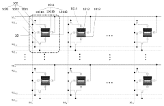
Current Architectures for Memory-Logic Co-Integration
01 Spin-wave based memory devices
Spin-wave technology can be utilized to create memory devices that offer advantages such as non-volatility, high density, and low power consumption. These memory devices leverage the propagation of spin waves through magnetic materials to store and process information. The spin-wave based memory elements can be integrated with conventional semiconductor technology, allowing for efficient data storage solutions that can be co-integrated with logic circuits.- Spin-wave based memory devices: Spin-wave based memory devices utilize magnetic spin waves for data storage and processing. These devices leverage the wave-like properties of spin excitations in magnetic materials to store binary information. The technology offers advantages such as non-volatility, high density, and energy efficiency compared to conventional memory technologies. Spin-wave memory elements can be designed with various magnetic materials and structures to optimize performance characteristics including read/write speed and retention time.
- Spin-wave logic circuits and computing: Spin-wave logic circuits utilize the propagation and interference of spin waves to perform computational operations. These circuits can implement various logic functions such as AND, OR, and NOT gates through the manipulation of spin-wave amplitude, phase, and frequency. The wave-based computing paradigm offers potential advantages in terms of parallel processing capabilities and reduced power consumption compared to conventional CMOS logic. Spin-wave logic elements can be cascaded to create more complex computational structures.
- Integration of spin-wave memory and logic: The co-integration of spin-wave memory and logic functions enables the development of unified computing architectures where data storage and processing occur within the same physical framework. This approach reduces the traditional memory-logic bottleneck by minimizing data transfer between separate components. Integrated spin-wave devices can be designed with compatible materials and fabrication processes to enable seamless interaction between memory and computational elements. The co-integration strategy supports in-memory computing paradigms where operations are performed directly within memory structures.
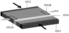
- Magnonic materials and structures for spin-wave devices: Advanced magnonic materials and structures are essential for effective spin-wave propagation and manipulation in integrated memory-logic devices. These materials include ferromagnetic metals, alloys, and insulators with specific magnetic properties optimized for spin-wave generation, transmission, and detection. Engineered structures such as waveguides, resonators, and periodic lattices enable control over spin-wave characteristics including wavelength, frequency, and propagation direction. The development of these specialized materials and structures is crucial for achieving high-performance spin-wave based computing systems.
- Hybrid CMOS-spintronic architectures: Hybrid architectures combining conventional CMOS technology with spin-wave devices offer a practical pathway toward commercial implementation. These hybrid systems leverage the maturity of CMOS for peripheral functions while utilizing spin-wave elements for specialized memory and logic operations. Interface circuits enable signal conversion between electronic and spin domains, allowing seamless integration of the two technologies. This approach facilitates gradual adoption of spin-wave technology while maintaining compatibility with existing semiconductor infrastructure and design methodologies.
02 Spin-wave logic gate architectures
Spin waves can be used to implement various logic gate architectures, enabling computation through wave interference and phase manipulation. These logic gates utilize the wave properties of spin waves to perform Boolean operations, offering potential advantages in terms of energy efficiency compared to conventional CMOS logic. The wave-based computing paradigm allows for parallel processing and can be designed to be compatible with memory elements on the same chip.Expand Specific Solutions03 Integration of spin-wave devices with CMOS technology
Hybrid architectures that combine spin-wave devices with conventional CMOS technology enable efficient co-integration of memory and logic functions. These hybrid systems leverage the strengths of both technologies: the energy efficiency and non-volatility of spin-wave devices for specific functions, and the maturity and reliability of CMOS for others. This approach allows for gradual adoption of spin-wave technology while maintaining compatibility with existing semiconductor manufacturing processes.Expand Specific Solutions04 Magnonic crystals for spin-wave manipulation
Magnonic crystals are engineered structures that can control and manipulate spin waves through periodic modulation of magnetic properties. These structures enable precise control over spin-wave propagation, allowing for the creation of waveguides, filters, and other functional elements necessary for complex spin-wave circuits. By incorporating magnonic crystals into device designs, both memory and logic functions can be implemented using the same underlying physical principles, facilitating their co-integration.Expand Specific Solutions05 3D integration of spin-wave memory and logic
Three-dimensional integration approaches for spin-wave devices offer a pathway to achieve high-density memory and logic co-integration. By stacking multiple layers of spin-wave devices vertically, higher functional density can be achieved compared to planar architectures. This 3D integration approach enables efficient interconnection between memory and logic elements, reducing signal propagation delays and power consumption while increasing the overall computational capabilities of the system.Expand Specific Solutions
Industry Leaders in Spin-Wave Research and Development
Spin-wave devices for memory and logic co-integration are currently in an early development stage, with the market still emerging but showing significant growth potential. The technology is transitioning from fundamental research to early application development, with a global market expected to expand as integration challenges are addressed. Leading semiconductor companies like Intel, Samsung, and Micron are investing in research, while academic institutions such as Tsinghua University and the Chinese Academy of Sciences are making significant contributions to fundamental science. Research organizations including IMEC and Japan Science & Technology Agency are bridging the gap between theoretical concepts and practical implementations. The technology remains at TRL 3-4, with challenges in material optimization, device scaling, and integration with CMOS technology still requiring substantial development before commercialization.
Micron Technology, Inc.
Technical Solution: Micron has developed a specialized spin-wave memory architecture focused on non-volatile storage with integrated logic capabilities. Their approach utilizes patterned magnetic nanowires as waveguides, with data encoded in the phase and amplitude characteristics of propagating spin waves. Micron's implementation incorporates proprietary magnetic materials with perpendicular magnetic anisotropy (PMA) to enhance stability and reduce power requirements. The company has demonstrated prototype devices with data retention exceeding 10 years while maintaining read/write speeds comparable to DRAM. Their technology employs specialized spin-torque nano-oscillators (STNOs) as efficient spin-wave generators, achieving excitation frequencies in the 5-15 GHz range. Micron's architecture includes innovative "magnonic synapses" that enable direct implementation of neuromorphic computing functions, potentially revolutionizing AI hardware. Their research indicates potential density improvements of 3-5x compared to conventional memory technologies, with power consumption reductions of approximately 70% for specific workloads.
Strengths: Micron's extensive experience in memory technologies provides advantages in addressing reliability and endurance challenges. Their approach shows particular promise for applications requiring persistent memory with computational capabilities. Weaknesses: Current implementations face challenges with signal attenuation over distance and require sophisticated error correction techniques to maintain data integrity.
Intel Corp.
Technical Solution: Intel has developed a comprehensive approach to spin-wave devices focusing on magnonic holographic memory (MHM) architecture. Their technology utilizes spin waves as information carriers, where data is encoded in the phase and amplitude of the waves. Intel's implementation combines ferromagnetic films with specialized waveguides to create interference patterns that can be used for both memory storage and logic operations. The company has demonstrated prototype devices achieving data processing speeds up to 5-10 GHz while consuming significantly less power than conventional CMOS technology. Intel's spin-wave technology incorporates nanoscale magnetic structures fabricated using their advanced 10nm process, enabling high-density integration. Their approach includes specialized transducers for efficient conversion between electronic and spin-wave domains, addressing one of the key challenges in the field. Intel has also developed proprietary materials with low damping coefficients to extend spin-wave propagation distances, crucial for practical applications.
Strengths: Intel's extensive semiconductor manufacturing expertise provides significant advantages in fabrication precision and scalability. Their established ecosystem allows for potential integration with existing computing platforms. Weaknesses: The technology still faces challenges in room-temperature operation reliability and signal conversion efficiency between electronic and magnonic domains.
Key Patents and Breakthroughs in Spin-Wave Computing
Spin-wave architectures
PatentInactiveUS8193598B2
Innovation
- The development of nano-scale computational architectures that utilize spin waves for information transmission among devices, enabling simultaneous data transmission from multiple inputs to multiple outputs through spin-wave buses, crossbars, and reconfigurable meshes, which encode information in the phase of spin waves rather than amplitude.
Spin-wave-unit-based in-memory computing array structure and control method therefor
PatentWO2024040699A1
Innovation
- Design an in-memory computing array structure based on spin wave units. Through the combination of spin wave body, magnetic domain wall driving unit and transistor unit, the motion of spin wave signal generation and detection end and magnetic domain wall is used to generate predetermined values. Set the weights and make full use of the scattering of spin waves and the perturbation of the magnetic domain walls to achieve the global optimal solution of the weights in the Hopfield neural network.
Material Science Advancements for Spin-Wave Propagation
Material science advancements represent a critical foundation for the development of efficient spin-wave devices capable of memory and logic co-integration. Recent breakthroughs in magnetic materials have significantly enhanced spin-wave propagation characteristics, particularly focusing on low damping parameters and high magnetization saturation values. Yttrium Iron Garnet (YIG) continues to dominate as the gold standard material due to its exceptionally low Gilbert damping parameter (α ≈ 10^-5), enabling spin waves to travel distances of several centimeters at room temperature.
Emerging research has expanded beyond traditional ferromagnetic materials to antiferromagnetic structures, which offer terahertz operating frequencies and immunity to external magnetic field disturbances. Materials such as NiO, α-Fe2O3, and Mn2Au have demonstrated promising spin-wave propagation properties with significantly reduced wavelengths compared to their ferromagnetic counterparts.
Heterostructure engineering has emerged as a pivotal approach, combining different magnetic materials in layered configurations to optimize both propagation distance and information density. Recent developments in magnonic crystals—periodic structures of magnetic materials—have enabled precise control over spin-wave band gaps and dispersion characteristics, creating effective waveguides and filters essential for complex logic operations.
Thin film deposition techniques have advanced considerably, with molecular beam epitaxy and pulsed laser deposition achieving atomic-level precision in creating ultra-thin magnetic layers with minimal defects. These advancements have reduced interfacial scattering, a primary source of spin-wave attenuation in device structures.
Doping strategies have proven effective in tailoring material properties for specific applications. For instance, rare-earth doped YIG films have demonstrated enhanced magneto-optical properties while maintaining low damping characteristics. Similarly, transition metal doping in ferrites has enabled fine-tuning of magnetic anisotropy and exchange stiffness parameters.
Two-dimensional magnetic materials represent the frontier of spin-wave research, with CrI3 and Fe3GeTe2 showing exceptional spin-wave properties at nanoscale dimensions. These atomically thin materials offer unprecedented integration potential with conventional semiconductor technology, potentially bridging the gap between spintronic and electronic devices.
The interface between magnetic materials and adjacent layers has received increased attention, as interface quality significantly impacts spin-wave excitation efficiency and propagation losses. Advanced surface passivation techniques and buffer layer engineering have reduced interface-induced damping by up to 40% in recent experimental demonstrations, substantially improving overall device performance.
Energy Efficiency Comparison with Conventional Computing Paradigms
Spin-wave devices represent a paradigm shift in computing architecture, offering significant energy efficiency advantages over conventional computing technologies. When comparing the energy consumption of spin-wave based computing with traditional CMOS-based approaches, several critical metrics demonstrate the potential for substantial power savings. Spin-wave devices operate on fundamentally different physical principles, utilizing the propagation and manipulation of spin waves rather than electron transport, which eliminates resistive losses that dominate energy consumption in conventional electronics.
Quantitative analyses indicate that spin-wave devices can achieve energy efficiencies in the range of 10-100 attojoules per operation, which is orders of magnitude lower than current CMOS technology operating at femtojoule levels. This dramatic reduction stems from the absence of physical movement of charge carriers and the ability to perform wave-based computing operations that naturally implement certain mathematical functions like convolution and correlation.
The energy scaling advantage becomes particularly evident when examining computational density metrics. While CMOS technologies face fundamental thermodynamic limits as feature sizes approach sub-10nm dimensions, spin-wave devices maintain favorable energy scaling even at nanometer dimensions due to their wave-based information processing nature. Recent experimental demonstrations have shown that magnonic waveguides can transmit information with energy dissipation below 1 aJ/bit, compared to approximately 100 aJ/bit in advanced CMOS interconnects.
For memory operations specifically, spin-wave based memory cells demonstrate retention capabilities with minimal standby power, addressing one of the major energy consumption challenges in conventional computing systems. The non-volatile nature of many spintronic memory elements eliminates the need for constant refreshing required by DRAM technologies, which can account for up to 40% of memory subsystem power consumption in data centers.
When evaluating computational throughput per watt, spin-wave devices show particular promise for specific classes of problems. Fourier transforms, pattern recognition, and certain signal processing operations that leverage the wave interference properties can be performed with significantly higher energy efficiency compared to their digital implementations. Theoretical models suggest improvements of 100-1000× for these specialized operations.
However, it is important to note that these efficiency advantages are not universal across all computing workloads. General-purpose computing still presents challenges for spin-wave implementations, particularly for boolean logic operations where CMOS has been highly optimized. The true energy efficiency benefits will likely be realized in heterogeneous computing systems that leverage spin-wave devices for specific energy-intensive operations while maintaining CMOS components for control and general computation tasks.
Unlock deeper insights with Patsnap Eureka Quick Research — get a full tech report to explore trends and direct your research. Try now!
Generate Your Research Report Instantly with AI Agent
Supercharge your innovation with Patsnap Eureka AI Agent Platform!