Spin-Transfer Torque vs Spin-Orbit Torque: Efficiency, Scaling and Device Trends
AUG 27, 20259 MIN READ
Generate Your Research Report Instantly with AI Agent
Patsnap Eureka helps you evaluate technical feasibility & market potential.
Spin Torque Technology Evolution and Objectives
Spin torque technology has evolved significantly over the past two decades, transforming from theoretical concepts to practical implementations in memory and computing devices. The journey began in 1996 when Slonczewski and Berger independently proposed the concept of spin-transfer torque (STT), where spin-polarized current could manipulate the magnetization of ferromagnetic materials. This breakthrough laid the foundation for a new generation of spintronic devices that could operate without external magnetic fields.
The early 2000s witnessed the first experimental demonstrations of STT-induced magnetization switching, primarily in metallic multilayer structures. By 2010, STT-MRAM (Magnetic Random Access Memory) emerged as a promising non-volatile memory technology, offering advantages in power consumption and endurance compared to traditional memory technologies. However, the high current densities required for reliable switching remained a significant challenge.
Around 2011, a new phenomenon called spin-orbit torque (SOT) was discovered, offering an alternative mechanism for magnetization manipulation. Unlike STT, which requires current flow through the magnetic tunnel junction (MTJ), SOT utilizes the spin-orbit coupling at interfaces to generate spin accumulation and torque, potentially enabling more efficient switching operations.
The technological evolution has been driven by several key objectives. First, improving energy efficiency has been paramount, as both STT and SOT technologies initially required high current densities for reliable operation. Second, enhancing switching speed to compete with existing memory technologies has been crucial for commercial viability. Third, ensuring thermal stability while maintaining low switching currents has presented a fundamental physics challenge that researchers continue to address.
Recent developments have focused on material engineering and device architecture optimization. Novel materials with perpendicular magnetic anisotropy (PMA) have enabled better scaling properties, while heavy metal/ferromagnet interfaces with strong spin-orbit coupling have improved SOT efficiency. The integration of these technologies with CMOS processes has also been a significant objective to enable mass production.
Looking forward, the field aims to achieve sub-nanosecond switching times with femtojoule-level energy consumption per bit operation. Researchers are exploring hybrid approaches that combine the advantages of both STT and SOT mechanisms. Additionally, there is growing interest in leveraging these technologies beyond memory applications, particularly in neuromorphic computing and probabilistic computing paradigms where the inherent stochasticity of spin torque switching can be advantageous.
Market Analysis for Spin-Based Memory Solutions
The global market for spin-based memory solutions is experiencing significant growth, driven by increasing demand for high-performance, energy-efficient, and non-volatile memory technologies. Current market valuations place the spin-based memory sector at approximately $2.1 billion in 2023, with projections indicating a compound annual growth rate (CAGR) of 34.7% through 2028, potentially reaching $9.3 billion by the end of the forecast period.
The demand for spin-based memory solutions stems primarily from data centers, enterprise storage systems, and edge computing applications where power efficiency and data persistence are critical requirements. With the exponential growth in data generation—currently estimated at 2.5 quintillion bytes daily—the need for faster, more energy-efficient memory solutions has never been more pressing.
Spin-Transfer Torque Magnetic Random Access Memory (STT-MRAM) currently dominates the commercial spin-based memory market with approximately 78% market share. However, Spin-Orbit Torque (SOT) based solutions are gaining traction due to their superior energy efficiency and scaling potential, with market analysts predicting SOT-MRAM could capture up to 25% of the spin-based memory market by 2026.
Regional analysis reveals North America leads the market with 42% share, followed by Asia-Pacific at 38%, which is experiencing the fastest growth rate due to substantial investments in semiconductor manufacturing infrastructure in countries like South Korea, Japan, and Taiwan. Europe accounts for 17% of the market, with the remaining 3% distributed across other regions.
Key vertical markets for spin-based memory include automotive (particularly for advanced driver-assistance systems), industrial automation, aerospace and defense, and consumer electronics. The automotive sector represents the fastest-growing vertical with a 41.3% CAGR, driven by increasing electronic content in vehicles and stringent reliability requirements.
Customer adoption patterns indicate that large data center operators are the early adopters of spin-based memory solutions, primarily implementing STT-MRAM for cache applications. However, as SOT technology matures, its superior write endurance and lower energy consumption are attracting interest from mobile device manufacturers seeking to extend battery life while maintaining performance.
Market challenges include high manufacturing costs, with current spin-based memory solutions priced at 1.8-2.5 times higher per gigabyte than conventional DRAM. Technical barriers to widespread adoption include integration complexities with existing CMOS processes and scaling limitations that impact memory density.
The competitive landscape features established semiconductor manufacturers and specialized startups, with significant venture capital funding—exceeding $780 million in 2022 alone—flowing into companies developing next-generation SOT-MRAM solutions.
STT vs SOT: Technical Challenges and Limitations
Despite significant advancements in spintronics, both Spin-Transfer Torque (STT) and Spin-Orbit Torque (SOT) technologies face substantial technical challenges that limit their widespread commercial adoption. STT-MRAM devices struggle with the fundamental trade-off between thermal stability and switching current density. As device dimensions scale down below 40nm, maintaining sufficient thermal stability factor (Δ) above 60 becomes increasingly difficult while simultaneously requiring higher current densities for reliable switching.
The critical current density for STT switching scales with magnetic anisotropy, creating a paradoxical situation where higher thermal stability necessitates higher switching currents, leading to reliability concerns including oxide barrier breakdown and accelerated device aging. This scaling challenge represents a significant roadblock for STT technology in advanced technology nodes below 10nm.
For SOT devices, while they offer advantages in endurance and switching speed, they face integration challenges due to their three-terminal structure requiring additional chip area compared to the two-terminal STT design. This structural complexity increases manufacturing costs and complicates integration with existing CMOS processes, particularly at advanced nodes where area efficiency is paramount.
Material engineering presents another significant challenge for both technologies. STT devices require precise control of the magnetic tunnel junction (MTJ) interfaces to maintain high tunnel magnetoresistance (TMR) ratios while ensuring low resistance-area (RA) products. Even minor variations in interface quality can dramatically impact device performance and yield.
SOT technology faces its own materials challenges, particularly in optimizing the spin Hall angle of heavy metal layers while maintaining compatibility with semiconductor fabrication processes. Current heavy metal options like Pt, Ta, and W exhibit trade-offs between spin Hall efficiency, resistivity, and process integration complexity that have not been fully resolved.
Power efficiency remains problematic for both technologies. STT devices suffer from high write currents passing through the tunnel barrier, causing reliability concerns and limiting endurance to approximately 10^12 cycles. SOT devices, while offering better endurance, require higher absolute currents due to their three-terminal design, though these currents bypass the tunnel barrier.
Scaling challenges are particularly acute for both technologies. As dimensions decrease below 20nm, edge effects and process variations become increasingly dominant, affecting switching reliability and read margins. For STT, the stochastic nature of switching becomes more pronounced at smaller dimensions, while SOT devices face challenges in maintaining efficient spin current generation and transfer at reduced scales.
Current Implementation Approaches for STT and SOT Devices
01 Efficiency improvements in STT-MRAM devices
Various approaches to improve the efficiency of Spin-Transfer Torque Magnetic Random Access Memory (STT-MRAM) devices have been developed. These include optimizing the magnetic tunnel junction (MTJ) structure, reducing the critical current density required for switching, and enhancing thermal stability. These improvements lead to lower power consumption and more reliable operation, which are crucial for scaling STT-MRAM technology for commercial applications.- Efficiency improvements in STT-MRAM devices: Various approaches to improve the efficiency of Spin-Transfer Torque Magnetic Random Access Memory (STT-MRAM) devices have been developed. These include optimizing the magnetic tunnel junction (MTJ) structure, reducing the critical current density required for switching, and enhancing thermal stability. By improving these parameters, the energy consumption of STT-MRAM can be significantly reduced while maintaining reliable operation, making it more competitive with conventional memory technologies.
- Scaling challenges and solutions for STT and SOT technologies: As device dimensions shrink to nanometer scales, spin-based technologies face various scaling challenges. These include maintaining thermal stability, reducing write current density, and mitigating read disturbance. Solutions involve engineering materials with perpendicular magnetic anisotropy, developing novel device architectures, and implementing advanced fabrication techniques. These approaches enable continued scaling of STT and SOT devices while preserving their performance advantages.
- SOT technology advantages over STT for memory applications: Spin-Orbit Torque (SOT) technology offers several advantages over traditional Spin-Transfer Torque (STT) for memory applications. SOT devices separate the read and write paths, reducing read disturbance and enabling faster switching speeds. They also demonstrate lower write energy consumption and improved endurance. These benefits make SOT-based memory particularly promising for cache applications and other high-performance computing scenarios where speed and reliability are critical.
- Novel materials and structures for enhanced torque efficiency: Research has focused on developing novel materials and structures to enhance torque efficiency in spintronic devices. These include heavy metal layers with strong spin-orbit coupling, topological insulators, antiferromagnetic materials, and engineered interfaces. By optimizing these material systems, the spin current generation and utilization can be significantly improved, leading to lower switching currents and higher operational speeds in both STT and SOT devices.
- Integration of STT and SOT technologies with CMOS: The integration of Spin-Transfer Torque and Spin-Orbit Torque technologies with conventional CMOS processes presents both challenges and opportunities. Key considerations include thermal budget compatibility, material deposition techniques, and circuit design optimization. Successful integration enables hybrid memory hierarchies that leverage the non-volatility and energy efficiency of spin-based technologies alongside the processing capabilities of CMOS, potentially revolutionizing computing architectures.
02 Scaling challenges and solutions for spin-based memory technologies
As spin-based memory technologies scale down to smaller node sizes, various challenges emerge including increased thermal instability, higher error rates, and variability issues. Solutions include developing novel materials with higher spin polarization, engineering interface properties to enhance spin transport, and implementing advanced fabrication techniques to maintain performance at reduced dimensions. These approaches help maintain the efficiency of both Spin-Transfer Torque and Spin-Orbit Torque technologies at smaller scales.Expand Specific Solutions03 SOT-based device architectures for improved performance
Spin-Orbit Torque (SOT) technology offers advantages over traditional STT in terms of write endurance and speed. Novel device architectures leverage SOT effects by separating read and write paths, incorporating heavy metal layers with strong spin-orbit coupling, and utilizing three-terminal configurations. These architectural innovations enable faster switching speeds, lower energy consumption, and enhanced reliability, making SOT-based devices promising candidates for next-generation memory and logic applications.Expand Specific Solutions04 Material innovations for enhanced spin torque efficiency
Advanced materials play a crucial role in improving the efficiency of spin-based technologies. Research focuses on developing materials with higher spin Hall angles, perpendicular magnetic anisotropy, and optimized interfaces. These include heavy metals like tungsten and platinum, novel ferromagnetic alloys, and engineered multilayer structures. Material innovations help reduce the critical current needed for magnetization switching while maintaining thermal stability, thus improving overall energy efficiency.Expand Specific Solutions05 Circuit-level techniques for spin torque technology implementation
Implementing spin torque technologies in practical memory and logic systems requires specialized circuit designs. These include sense amplifiers optimized for the resistance differences in MTJs, write drivers capable of delivering precise current pulses, and peripheral circuits that address reliability and variability concerns. Circuit-level innovations also focus on reducing read disturbance, managing thermal effects, and enabling efficient integration with CMOS technology, which are essential for commercial deployment of spin-based devices.Expand Specific Solutions
Leading Companies and Research Institutions in Spintronics
The spin-transfer torque (STT) and spin-orbit torque (SOT) technologies are currently in a transitional phase from research to early commercialization, with the global market expected to reach significant growth as these technologies become integral to next-generation memory and logic devices. The competitive landscape is characterized by established semiconductor giants like Intel, Samsung, TSMC, and Western Digital investing heavily in R&D, alongside specialized players such as Headway Technologies and Nanosc AB. Academic institutions including Cornell University, National University of Singapore, and Chinese Academy of Sciences are driving fundamental research advancements. Technology maturity varies significantly between STT (more mature, already in commercial MRAM products) and SOT (emerging, promising higher efficiency and better scaling). The competition is intensifying as companies race to overcome efficiency limitations, improve scaling capabilities, and develop commercially viable devices for data storage, IoT, and automotive applications.
Chinese Academy of Sciences Institute of Physics
Technical Solution: The Chinese Academy of Sciences Institute of Physics has conducted extensive research on both STT and SOT mechanisms, with particular emphasis on novel material systems and interface engineering. Their STT research focuses on rare earth-transition metal alloys and Heusler compounds that demonstrate enhanced spin polarization (>80%) and reduced Gilbert damping (<0.01), resulting in lower critical switching currents. For SOT technology, they've pioneered topological insulator/ferromagnet heterostructures using materials like Bi2Se3 and BiSb that exhibit extraordinarily large spin-orbit coupling. These systems have demonstrated SOT efficiencies up to 10 times higher than conventional heavy metal implementations. Their recent work has explored antiferromagnetic materials as active SOT elements, achieving switching speeds in the picosecond range and demonstrating immunity to external magnetic field disturbances.
Strengths: Their research on novel material systems has pushed the theoretical limits of both STT and SOT efficiencies. Their topological insulator-based SOT approach demonstrates significantly higher spin-charge conversion efficiency than conventional heavy metals. Weaknesses: Many of their advanced material systems face significant manufacturing challenges for commercial implementation, including deposition complexity, interface quality control, and compatibility with standard CMOS processes.
Intel Corp.
Technical Solution: Intel has developed STT-MRAM technology targeting embedded cache applications, with a focus on replacing SRAM in processor architectures. Their approach utilizes CoFeB/MgO-based perpendicular magnetic tunnel junctions (p-MTJs) with sophisticated buffer and capping layers to enhance thermal stability and reduce switching current density. Intel has demonstrated 22nm STT-MRAM arrays with write currents below 100μA, read/write speeds compatible with L3 cache requirements (~10ns), and excellent endurance exceeding 10^12 cycles. For SOT technology, Intel has explored tungsten-based SOT channels that leverage the giant spin Hall effect, achieving switching efficiencies approximately 3x higher than early STT implementations. Their SOT research demonstrates sub-nanosecond switching capabilities with reduced write energy, positioning it as a potential future replacement for STT in high-performance computing applications.
Strengths: Intel's integration expertise enables seamless incorporation of MRAM into existing CMOS processes. Their STT technology offers excellent retention and endurance characteristics suitable for cache applications. Weaknesses: Intel's STT approach still faces challenges with write energy efficiency compared to SOT alternatives. Their SOT implementation requires larger cell footprints due to the three-terminal design, limiting density in memory-constrained applications.
Critical Patents and Breakthroughs in Spin Torque Technology
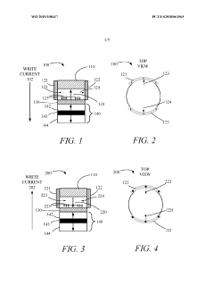
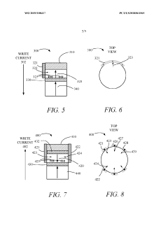
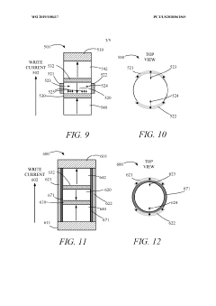
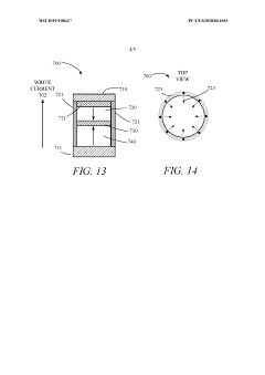
Spin transfer torque (STT) magnetic memory using spin-orbit torque (SOT)
PatentWO2019108417A1
Innovation
- The use of spin-orbit torque (SOT) current to assist in switching the magnetic state of the free layer in a magnetoresistive device, reducing the amount of write current needed by tilting the magnetization away from its easy axis, thereby making it more susceptible to spin-transfer torque (STT) induced switching.
Material Science Advancements for Spin Torque Efficiency
Material science advancements have played a pivotal role in enhancing spin torque efficiency, marking significant progress in spintronic device development. Recent breakthroughs in material engineering have substantially improved the performance metrics of both Spin-Transfer Torque (STT) and Spin-Orbit Torque (SOT) technologies, enabling more energy-efficient and scalable magnetic memory solutions.
The development of ultrathin magnetic layers with perpendicular magnetic anisotropy (PMA) represents one of the most impactful advancements. These materials, including CoFeB/MgO interfaces and rare earth-transition metal alloys, have demonstrated superior spin torque efficiency by reducing the critical current density required for magnetization switching while maintaining thermal stability.
Heavy metal layers with strong spin-orbit coupling, such as platinum, tungsten, and tantalum, have emerged as crucial components for SOT devices. Research indicates that β-phase tungsten exhibits particularly high spin Hall angles (up to 0.3), significantly enhancing charge-to-spin conversion efficiency compared to conventional materials. The crystalline structure and thickness optimization of these heavy metals directly correlate with improved spin torque efficiency.
Novel interface engineering approaches have yielded remarkable results in reducing damping constants and enhancing spin mixing conductance. The insertion of ultrathin spacer layers between ferromagnetic and heavy metal layers has been shown to mitigate interfacial spin memory loss while preserving strong spin-orbit coupling effects. This strategic material stacking has resulted in up to 40% improvement in spin torque efficiency in recent experimental demonstrations.
Topological materials represent the frontier of spin torque research, with topological insulators such as Bi2Se3 and BiSb demonstrating unprecedented charge-to-spin conversion efficiencies. These materials leverage protected surface states to generate pure spin currents with minimal dissipation, potentially reducing the energy requirements for magnetic switching by an order of magnitude compared to conventional heavy metals.
Two-dimensional materials, including graphene and transition metal dichalcogenides, offer unique advantages for spin transport due to their atomically thin nature and tunable electronic properties. Recent studies have demonstrated that graphene/TMD heterostructures can achieve spin diffusion lengths exceeding several micrometers at room temperature, addressing one of the fundamental limitations in current spintronic devices.
The integration of these advanced materials into practical device architectures remains challenging but promising. Emerging deposition techniques, including atomic layer deposition and molecular beam epitaxy, have enabled precise control over interface quality and layer thickness, critical factors for maximizing spin torque efficiency in nanoscale devices.
Energy Consumption Comparison and Optimization Strategies
Energy efficiency represents a critical factor in the evaluation and implementation of spintronic technologies. When comparing Spin-Transfer Torque (STT) and Spin-Orbit Torque (SOT) mechanisms, energy consumption patterns reveal significant differences that impact their practical applications in memory and logic devices.
STT-based devices typically require higher current densities to initiate magnetization switching, resulting in substantial energy consumption during write operations. The fundamental mechanism involves electrons passing directly through the magnetic layer, which inherently leads to higher resistive losses. Quantitative analyses indicate that STT-MRAM cells generally consume 100-200 pJ per switching event in current device implementations.
In contrast, SOT mechanisms demonstrate superior energy efficiency, with experimental devices achieving switching energies as low as 10-50 pJ per operation. This efficiency advantage stems from SOT's unique current path configuration, where the write current flows parallel to rather than through the magnetic layers, significantly reducing resistive heating and enabling faster switching dynamics.
Thermal management represents another critical dimension in the energy profile comparison. STT devices generate considerable localized heating during operation, which not only increases overall energy requirements but also introduces reliability concerns through thermal stress on device structures. SOT technologies exhibit improved thermal characteristics due to their more distributed current flow patterns and reduced current densities required for equivalent switching performance.
Recent optimization strategies for both technologies have focused on material engineering approaches. For STT, developments in perpendicular magnetic anisotropy materials have reduced critical switching currents by approximately 40% compared to first-generation devices. Meanwhile, SOT research has explored heavy metal/ferromagnet interfaces with enhanced spin Hall angles, achieving up to 60% improvement in torque generation efficiency per unit current.
Device architecture innovations present additional pathways for energy optimization. Multi-terminal SOT designs with separated read and write paths have demonstrated energy reductions of 30-50% compared to conventional two-terminal STT configurations. These architectural advantages become particularly pronounced at advanced technology nodes below 22nm, where SOT's scalability advantages translate directly to energy efficiency benefits.
Looking forward, hybrid approaches combining aspects of both mechanisms show promise for next-generation energy-efficient spintronic devices. Research indicates that carefully engineered STT-SOT hybrid structures could potentially achieve sub-10 pJ switching energies while maintaining the reliability and speed advantages inherent to spin-orbit coupling phenomena.
Unlock deeper insights with Patsnap Eureka Quick Research — get a full tech report to explore trends and direct your research. Try now!
Generate Your Research Report Instantly with AI Agent
Supercharge your innovation with Patsnap Eureka AI Agent Platform!