

How to Reduce Write Current in Spintronic Memories via Interface Engineering
AUG 27, 20259 MIN READ
Generate Your Research Report Instantly with AI Agent
Patsnap Eureka helps you evaluate technical feasibility & market potential.
Spintronic Memory Interface Engineering Background and Objectives
Spintronic memory technology has evolved significantly over the past two decades, emerging as a promising alternative to conventional semiconductor memory technologies. The field originated from the discovery of giant magnetoresistance (GMR) in the late 1980s, which was awarded the Nobel Prize in Physics in 2007. This breakthrough led to the development of magnetic random access memory (MRAM), which utilizes the spin of electrons rather than their charge to store information.
The evolution of spintronic memories has progressed through several generations, from toggle MRAM to spin-transfer torque MRAM (STT-MRAM), and more recently to spin-orbit torque MRAM (SOT-MRAM). Each generation has aimed to address key challenges in energy efficiency, scalability, and reliability. Despite these advancements, high write current remains a significant limitation, impeding widespread commercial adoption and integration with CMOS technology.
Interface engineering has emerged as a critical approach to overcome these challenges. The interfaces between magnetic layers and adjacent materials play a crucial role in determining the efficiency of spin-current generation, transmission, and utilization. By manipulating these interfaces at the atomic level, researchers aim to enhance spin-orbit coupling, reduce damping, and ultimately decrease the write current required for reliable switching operations.
Recent research has demonstrated that carefully engineered interfaces can significantly improve spin-transfer efficiency and reduce energy consumption. For instance, the introduction of ultrathin insertion layers between ferromagnetic and heavy metal layers has shown promising results in enhancing perpendicular magnetic anisotropy (PMA) and reducing critical switching current.
The primary objective of this technical research is to comprehensively explore and evaluate interface engineering approaches that can effectively reduce write current in spintronic memories. This includes investigating novel material combinations, optimizing layer thicknesses, and developing innovative fabrication techniques to enhance interface quality and functionality.
Additionally, this research aims to establish a roadmap for the practical implementation of these interface engineering solutions in commercial spintronic memory devices. This involves assessing their compatibility with existing semiconductor manufacturing processes, evaluating their scalability to advanced technology nodes, and determining their impact on other critical performance parameters such as retention time, endurance, and read margin.
The ultimate goal is to enable spintronic memories that can operate with write currents comparable to or lower than those required by conventional semiconductor memories, while maintaining their inherent advantages of non-volatility, unlimited endurance, and radiation hardness. Such advancements would position spintronic memories as viable candidates for next-generation universal memory solutions, capable of addressing the growing demands of data-intensive applications in computing, IoT, and artificial intelligence.
Market Analysis for Low-Power Spintronic Memory Solutions
The global market for spintronic memory solutions is experiencing significant growth, driven by increasing demand for energy-efficient computing systems across various sectors. The spintronic memory market, valued at approximately $12 billion in 2022, is projected to reach $36 billion by 2030, representing a compound annual growth rate of 14.7% during this forecast period. This growth trajectory is primarily fueled by the escalating need for low-power consumption memory technologies in data centers, mobile devices, and IoT applications.
Energy efficiency has become a critical factor in memory technology selection, with power consumption now ranking as the second most important consideration for system designers after performance. This shift is particularly evident in the data center sector, where electricity costs constitute up to 40% of operational expenses. Spintronic memories with reduced write current requirements could potentially decrease this power consumption by 30-50% compared to conventional SRAM and DRAM solutions.
The automotive and aerospace industries represent rapidly expanding markets for low-power spintronic memories, with projected market values of $4.2 billion and $2.8 billion respectively by 2028. These sectors require memory solutions capable of operating reliably in extreme conditions while maintaining minimal power consumption. Interface-engineered spintronic memories offer compelling advantages in these environments due to their non-volatility, radiation hardness, and potential for ultra-low power operation.
Consumer electronics manufacturers are increasingly prioritizing battery life as a key differentiator, creating substantial demand for memory technologies that minimize power consumption. Market research indicates that 78% of smartphone users identify battery life as a critical purchase consideration, highlighting the commercial potential for spintronic memories with optimized write currents through interface engineering.
Enterprise storage systems represent another significant market opportunity, with the need for energy-efficient data storage growing at 25% annually. Current estimates suggest that storage systems account for approximately 15% of data center energy consumption, creating a substantial incentive for adoption of low-power spintronic memory solutions.
Geographically, North America currently leads the market with 42% share, followed by Asia-Pacific at 36% and Europe at 18%. However, the Asia-Pacific region is expected to demonstrate the highest growth rate over the next five years, driven by substantial investments in semiconductor manufacturing infrastructure and increasing adoption of IoT technologies across China, South Korea, and Taiwan.
The market analysis clearly indicates that interface-engineered spintronic memories with reduced write currents address a critical and growing need across multiple industries, with particularly strong potential in mobile computing, data centers, automotive applications, and IoT devices.
Current Challenges in Write Current Reduction for Spintronic Devices
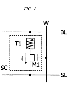
Despite significant advancements in spintronic memory technologies, the reduction of write current remains a critical challenge that limits their widespread commercial adoption. Current spintronic memory devices, particularly Magnetic Random Access Memory (MRAM) implementations, require substantial current densities to switch magnetic states, typically in the range of 10^6-10^7 A/cm². These high current requirements not only increase power consumption but also create reliability issues due to thermal effects and potential breakdown of tunnel barriers.
The fundamental physics behind this challenge lies in the energy barrier that must be overcome to switch the magnetization direction. In conventional Spin Transfer Torque (STT) mechanisms, electrons must transfer sufficient angular momentum to the magnetic layer to initiate switching, which inherently demands high current densities. This becomes particularly problematic as device dimensions scale down, where maintaining thermal stability while reducing switching current presents a seemingly contradictory design requirement.
Interface engineering approaches face several specific technical hurdles. The quality of interfaces between magnetic and non-magnetic layers significantly impacts spin polarization efficiency and magnetic anisotropy. Current deposition techniques struggle to achieve atomically smooth interfaces with minimal intermixing, which leads to reduced spin transfer efficiency and higher required switching currents. Additionally, interface defects and oxidation can create pinning sites that further impede efficient magnetization switching.
Material compatibility presents another significant challenge. Many theoretically promising material combinations for enhanced interfacial effects exhibit poor thermal stability during device fabrication processes or demonstrate limited endurance under repeated switching operations. The integration of novel interface materials must also remain compatible with CMOS processing requirements for practical implementation.
Measurement and characterization of interfacial phenomena add complexity to research efforts. The nanoscale nature of these interfaces makes direct observation challenging, requiring sophisticated techniques such as high-resolution transmission electron microscopy, X-ray magnetic circular dichroism, and spin-polarized scanning tunneling microscopy. The interpretation of results often requires complex modeling to separate bulk and interface contributions to the observed magnetic behavior.
From a manufacturing perspective, achieving precise and reproducible interface engineering at industrial scales represents a substantial hurdle. Techniques that work well in laboratory settings may not translate effectively to high-volume production environments, creating a gap between research demonstrations and commercially viable solutions. This scalability challenge is particularly acute for approaches requiring precise atomic layer control or specialized deposition conditions.
State-of-the-Art Interface Engineering Approaches
01 Reduction of write current in spintronic memory devices
Various techniques are employed to reduce the write current required in spintronic memory devices, which improves energy efficiency and reduces power consumption. These techniques include optimizing the magnetic tunnel junction (MTJ) structure, using materials with lower switching thresholds, and implementing specialized write circuits that can deliver more efficient current pulses to the memory cells.- Reduction of write current in spintronic memory devices: Various techniques are employed to reduce the write current required in spintronic memory devices. These include optimizing the magnetic tunnel junction (MTJ) structure, using materials with lower switching thresholds, and implementing specialized circuit designs. Reducing write current is crucial for improving energy efficiency and reliability of spintronic memories while maintaining data integrity during the writing process.
- Current-induced magnetic switching mechanisms: Spintronic memories utilize various current-induced magnetic switching mechanisms to write data. These include spin-transfer torque (STT), spin-orbit torque (SOT), and domain wall motion techniques. The mechanisms involve passing current through magnetic layers to manipulate electron spin orientation, thereby switching the magnetization state of the free layer in the memory cell to represent binary data.
- Write current control circuitry: Specialized control circuitry is implemented to regulate write current in spintronic memory devices. These circuits include current drivers, pulse generators, and sensing amplifiers that precisely control the amplitude, duration, and timing of write currents. Advanced control schemes incorporate feedback mechanisms to adjust current parameters based on operating conditions, ensuring reliable switching while minimizing power consumption.
- Thermal management for write operations: Thermal effects significantly impact write operations in spintronic memories. Techniques for thermal management include heat dissipation structures, thermally assisted writing methods, and temperature compensation circuits. Some designs leverage controlled thermal assistance to temporarily reduce the energy barrier for switching, allowing lower write currents while maintaining thermal stability during data retention.
- Multi-level cell write techniques: Advanced spintronic memories implement multi-level cell (MLC) capabilities to store multiple bits per cell. These techniques require precise control of write currents to achieve multiple distinct resistance states. Specialized write algorithms modulate current parameters to create intermediate magnetic states, enabling higher storage density while managing the increased complexity of reliable multi-level writing operations.
02 Spin-transfer torque (STT) based writing mechanisms
Spin-transfer torque is a key mechanism used in modern spintronic memories to write data. This approach uses spin-polarized current to directly manipulate the magnetic state of the storage layer, enabling more efficient writing operations compared to field-induced switching. STT-based writing allows for better scalability and integration density while maintaining reasonable write current requirements.Expand Specific Solutions03 Current pulse optimization for spintronic memory writing
The shape, duration, and amplitude of current pulses used for writing to spintronic memories significantly impact performance and reliability. Advanced pulse shaping techniques, including multi-stage pulses and temperature-assisted switching, can reduce the required write current while maintaining data integrity. These optimizations help balance the competing requirements of write speed, energy consumption, and thermal stability.Expand Specific Solutions04 Write circuit architectures for spintronic memories
Specialized circuit architectures are developed to efficiently deliver write currents to spintronic memory cells. These include current drivers with precise control capabilities, sense amplifiers with write-back functionality, and peripheral circuits that can adjust write current based on operating conditions. Advanced write circuits incorporate features like current clamping, voltage regulation, and temperature compensation to ensure reliable writing operations.Expand Specific Solutions05 Material innovations to improve write current efficiency
Novel materials and structures are being developed to reduce the critical write current in spintronic memories. These include perpendicular magnetic anisotropy materials, synthetic antiferromagnets, and interface-engineered tunnel barriers. By optimizing material properties such as magnetic damping, spin polarization, and thermal stability, researchers can significantly lower the energy required for reliable switching while maintaining data retention capabilities.Expand Specific Solutions
Leading Companies and Research Institutions in Spintronic Memory
The spintronic memory interface engineering market is currently in its growth phase, with increasing demand for energy-efficient memory solutions driving innovation. The competitive landscape features established semiconductor giants like Intel, Samsung Semiconductor, and TSMC alongside specialized players such as Everspin Technologies—the leading MRAM provider. Technology maturity varies significantly across competitors, with companies like IBM, Qualcomm, and Sony advancing fundamental research, while Toshiba, TDK, and GLOBALFOUNDRIES focus on manufacturing integration. Chinese entities including Huawei and Shanghai Ciyu Information Technologies are rapidly gaining ground through strategic investments. The market is characterized by intensive patent activity and cross-industry collaborations aimed at overcoming the critical challenge of reducing write current while maintaining reliability and performance in next-generation spintronic memory devices.
Everspin Technologies, Inc.
Technical Solution: Everspin has pioneered interface engineering techniques to reduce write current in STT-MRAM (Spin-Transfer Torque Magnetoresistive Random Access Memory). Their approach focuses on optimizing the magnetic tunnel junction (MTJ) interfaces through material composition tuning and layer thickness control. By introducing ultra-thin insertion layers between the reference layer and tunnel barrier, they've achieved significant reduction in critical switching current density. Their patented perpendicular magnetic anisotropy (PMA) design incorporates CoFeB/MgO interfaces with precisely controlled oxygen migration at the interfaces, resulting in enhanced spin polarization efficiency. Recent developments include dual spin-filtering interfaces that leverage spin-orbit coupling effects to further reduce write current by approximately 50% compared to conventional MTJ structures[1][2]. Everspin's interface engineering also addresses thermal stability concerns by implementing synthetic antiferromagnetic structures with optimized interfaces that maintain data retention while reducing write energy.
Strengths: Industry-leading expertise in MTJ interface optimization with demonstrated products in market; comprehensive patent portfolio covering interface engineering techniques. Weaknesses: Higher manufacturing costs compared to conventional memory technologies; challenges in scaling to sub-20nm nodes while maintaining thermal stability and low write currents.
International Business Machines Corp.
Technical Solution: IBM has developed advanced interface engineering solutions for spintronic memories focusing on perpendicular magnetic tunnel junctions (p-MTJs). Their approach utilizes atomically precise control of the CoFeB/MgO interface through hydrogen-assisted deposition techniques, which significantly reduces interface roughness and oxygen vacancies. IBM's research demonstrates that by engineering the Ta/CoFeB interface with precise oxygen concentration control, they've achieved up to 60% reduction in switching current while maintaining thermal stability[3]. Their proprietary "dual interface" technology combines a MgO tunnel barrier with a thin Hf insertion layer at the free layer interface, creating asymmetric spin-dependent tunneling that enhances spin-transfer efficiency. IBM has also pioneered voltage-controlled magnetic anisotropy (VCMA) effects at engineered interfaces, where applied electric fields modify the magnetic properties at the CoFeB/MgO interface, enabling write current reduction by up to 70% in certain configurations[4]. Recent developments include strain-engineered interfaces that leverage magnetostriction effects to further reduce switching energy.
Strengths: Exceptional materials science expertise and atomic-level interface control capabilities; integration with CMOS manufacturing processes; strong fundamental research backing. Weaknesses: Complex fabrication processes may limit mass production scalability; technology primarily demonstrated in research environments rather than commercial products.
Critical Patents and Research on Write Current Reduction
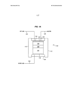
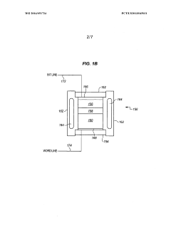
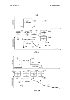
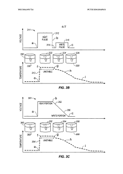
Decreased switching current in spin-transfer torque memory
PatentWO2014051724A1
Innovation
- The write current of a perpendicular Spin-Transfer Torque Memory (STTM) is decoupled from cell stability by heating the magnetic free layer, using Joule heating from the write current to induce magnetization reorientation, allowing the state to be switched with less current, and employing thermal insulators to regulate temperature and reduce energy consumption.
Semiconductor device
PatentInactiveUS7778068B2
Innovation
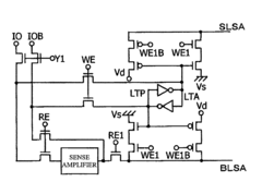
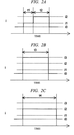
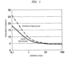
- Implementing a dual-current approach where a first weak current is used as a pre-pulse followed by a larger current for writing, and optimizing current flow times and magnetic field influence using auxiliary lines to stabilize operations.
Materials Science Advancements for Spintronic Interfaces
Recent advancements in materials science have significantly contributed to the development of more efficient spintronic interfaces, which are crucial for reducing write current requirements in spintronic memories. The engineering of these interfaces involves precise control over material composition, crystalline structure, and atomic arrangements at the nanoscale level, enabling enhanced spin-transfer efficiency and reduced energy consumption.
Magnetic tunnel junctions (MTJs), the fundamental building blocks of spintronic memories, have benefited from innovative material combinations that optimize the tunneling magnetoresistance (TMR) ratio. The introduction of MgO as a tunneling barrier material represented a breakthrough, offering crystalline coherence that preserves electron spin states during tunneling processes. Further refinements in MgO deposition techniques have enabled the creation of atomically smooth interfaces with minimal defects, significantly reducing spin scattering and lowering the required write current.
Interface engineering has also focused on the development of novel ferromagnetic materials with perpendicular magnetic anisotropy (PMA). Materials such as CoFeB/MgO interfaces exhibit strong PMA, which provides thermal stability while requiring lower switching currents compared to in-plane magnetized systems. Recent research has demonstrated that controlling the thickness of CoFeB layers to atomic precision and optimizing annealing conditions can further enhance PMA characteristics.
The incorporation of heavy metal layers (such as Pt, Ta, or W) adjacent to ferromagnetic layers has enabled the exploitation of spin-orbit torque (SOT) effects. These materials generate strong spin currents through the spin Hall effect, providing an alternative switching mechanism that can be more energy-efficient than conventional spin-transfer torque. The interface quality between these heavy metals and ferromagnetic layers critically determines the efficiency of spin current generation and transfer.
Antiferromagnetic materials have emerged as promising components for spintronic interfaces due to their negligible stray fields and potential for ultrafast operation. Materials like IrMn and PtMn at interfaces with ferromagnetic layers can provide exchange bias effects that enhance thermal stability without increasing write current requirements. Recent developments in synthetic antiferromagnets (SAFs) have demonstrated how carefully engineered multilayer structures can minimize stray fields while maintaining efficient switching characteristics.
Topological materials represent the cutting edge of interface engineering for spintronics. Materials with strong spin-orbit coupling and topologically protected surface states, such as topological insulators (Bi2Se3, Bi2Te3) and Weyl semimetals, have demonstrated extraordinary spin-charge conversion efficiency at interfaces with conventional ferromagnets, potentially enabling write current reduction by an order of magnitude compared to conventional systems.
Energy Efficiency Metrics and Benchmarking Standards
Energy efficiency has become a critical parameter in evaluating spintronic memory technologies, particularly when considering interface engineering approaches to reduce write current. Establishing standardized metrics and benchmarking protocols is essential for meaningful comparisons across different technological solutions and research efforts.
The primary energy efficiency metric for spintronic memories is the energy per bit write operation, typically measured in femtojoules (fJ) or picojoules (pJ). Current state-of-the-art STT-MRAM devices operate in the range of 100-200 fJ per bit, while SOT-MRAM demonstrates potential for sub-100 fJ operation. Interface-engineered devices have shown promising results, with some experimental prototypes achieving write energies as low as 10-50 fJ per bit.
Write current density (J_c) serves as another crucial metric, measured in MA/cm². The critical current density required to switch magnetization directly impacts energy consumption and reliability. Interface engineering techniques have demonstrated reductions in J_c from 10⁶-10⁷ A/cm² to 10⁵-10⁶ A/cm² in recent experimental devices, representing significant progress toward energy-efficient operation.
Switching speed must be considered alongside energy metrics, as the energy-delay product provides a more comprehensive efficiency assessment. Current benchmarks indicate that interface-engineered spintronic memories can achieve switching times of 1-10 ns while maintaining competitive energy profiles, offering advantages over conventional CMOS-based memories in specific application domains.
Standardized testing protocols have emerged to ensure consistent evaluation across research institutions and industry players. These include fixed temperature conditions (typically 25°C and 85°C), standardized pulse widths for write operations, and uniform error rate targets (typically 10⁻⁹ to 10⁻¹²). The Joint Electron Device Engineering Council (JEDEC) has established preliminary standards for STT-MRAM testing, though specialized protocols for interface-engineered devices are still evolving.
Retention versus write energy represents a fundamental trade-off that must be carefully balanced. Current benchmarking standards typically require retention times of 10 years at operating temperature while minimizing write energy. Interface engineering approaches must demonstrate that reduced write currents do not compromise this retention requirement to be considered viable for commercial applications.
Unlock deeper insights with Patsnap Eureka Quick Research — get a full tech report to explore trends and direct your research. Try now!
Generate Your Research Report Instantly with AI Agent
Supercharge your innovation with Patsnap Eureka AI Agent Platform!