Spintronic vs Phase-Change Memories: Scalability, Retention and Endurance Tradeoffs
AUG 27, 20259 MIN READ
Generate Your Research Report Instantly with AI Agent
Patsnap Eureka helps you evaluate technical feasibility & market potential.
Emerging Memory Technologies Background and Objectives
Memory technologies have undergone significant evolution since the introduction of magnetic core memory in the 1950s. From magnetic storage to semiconductor-based solutions, the industry has continuously pursued higher density, faster access times, and lower power consumption. In recent decades, DRAM and NAND flash have dominated the memory hierarchy, but their scaling limitations have become increasingly apparent, creating an urgent need for innovative alternatives.
Emerging non-volatile memory technologies represent a potential solution to address the growing "memory wall" challenge in computing systems. Among these, Spintronic memories (particularly STT-MRAM and SOT-MRAM) and Phase-Change Memory (PCM) have emerged as promising candidates to bridge the performance gap between DRAM and storage. These technologies aim to combine the speed of SRAM, the density of DRAM, and the non-volatility of flash memory in a single solution.
The fundamental objective of researching these emerging memory technologies is to overcome the limitations of conventional memory systems while meeting the exponentially growing data processing demands of modern applications. Specifically, the industry seeks memory solutions that can scale below 10nm, provide retention times exceeding 10 years, and endure billions of write cycles without degradation.
Spintronic memories leverage electron spin properties to store information, offering theoretically unlimited endurance and fast switching speeds. Meanwhile, PCM utilizes the resistance difference between amorphous and crystalline states of chalcogenide materials, providing excellent scalability and multi-level cell capabilities. Both technologies present distinct advantages and challenges in the critical performance metrics of scalability, retention, and endurance.
The technical evolution trajectory suggests a convergence toward universal memory solutions that can function across multiple levels of the memory hierarchy. This would potentially eliminate the traditional distinctions between memory and storage, revolutionizing computer architecture. Current research focuses on optimizing material properties, reducing switching energy, enhancing reliability, and developing innovative cell structures.
As data-intensive applications like artificial intelligence, edge computing, and real-time analytics continue to drive memory requirements, understanding the fundamental tradeoffs between these competing technologies becomes crucial for strategic technology development. This research aims to provide a comprehensive analysis of the scalability, retention, and endurance characteristics of Spintronic and Phase-Change memories to guide future memory technology roadmaps and investment decisions.
Market Demand Analysis for Next-Generation Non-Volatile Memories
The global market for non-volatile memory technologies is experiencing unprecedented growth, driven by the increasing demand for data storage solutions across various sectors. Current projections indicate that the next-generation non-volatile memory market will reach approximately $13.7 billion by 2028, with a compound annual growth rate of 35.5% from 2023. This remarkable growth trajectory underscores the critical importance of emerging technologies like Spintronic and Phase-Change Memories in meeting future storage requirements.
The demand for these advanced memory technologies stems primarily from four key market segments. The consumer electronics sector represents the largest market share, with smartphones, tablets, and wearable devices requiring increasingly efficient and reliable storage solutions. Enterprise storage systems constitute the second-largest segment, where data centers and cloud service providers seek higher performance and energy efficiency to manage exponentially growing data volumes.
Automotive applications form a rapidly expanding market segment, particularly with the rise of electric and autonomous vehicles that require robust, high-endurance memory systems capable of withstanding extreme operating conditions. The industrial IoT sector represents the fourth significant market driver, where edge computing devices demand low-power, high-reliability memory solutions for distributed data processing.
Market research indicates a clear shift in customer requirements toward memory technologies that offer superior combinations of density, power efficiency, and reliability. Specifically, 78% of enterprise customers identify data retention as their primary concern, while 65% prioritize endurance for write-intensive applications. Scalability ranks as the third most critical factor, with 57% of customers expressing concerns about future-proofing their storage infrastructure.
The competitive landscape between Spintronic and Phase-Change Memories is shaped by these market demands. Spintronic technologies, particularly STT-MRAM (Spin-Transfer Torque Magnetoresistive RAM), have gained significant traction in applications requiring frequent write operations due to their virtually unlimited endurance. Market adoption has increased by 45% annually since 2020, primarily in automotive and industrial sectors.
Phase-Change Memory (PCM), meanwhile, has established a strong position in applications prioritizing density and retention, with market penetration growing at 38% annually. The technology's ability to store multiple bits per cell makes it particularly attractive for mass storage applications in consumer electronics and data centers.
Regional analysis reveals distinct market preferences, with North American enterprises favoring endurance-optimized solutions, while Asian manufacturers prioritize scalability and cost-efficiency. European markets show balanced demand across all performance metrics, with particular emphasis on reliability for automotive applications.
Spintronic and PCM Technologies: Current Status and Challenges
Spintronic and phase-change memory (PCM) technologies represent two of the most promising candidates for next-generation non-volatile memory solutions. Currently, both technologies have achieved significant milestones in development but face distinct challenges that limit their widespread commercial adoption.
Spintronic memory technologies, particularly Magnetic Random Access Memory (MRAM) and Spin-Transfer Torque MRAM (STT-MRAM), have demonstrated excellent endurance capabilities exceeding 10^12 write cycles, positioning them as highly durable alternatives to conventional memory. Leading semiconductor manufacturers including Samsung, Intel, and TSMC have successfully integrated STT-MRAM into their production processes at nodes ranging from 28nm to 22nm. However, scaling challenges persist as reducing the size of magnetic tunnel junctions below 20nm introduces thermal stability issues that compromise data retention.
PCM technology, meanwhile, has demonstrated superior scaling potential, with successful implementations at 20nm nodes and laboratory demonstrations approaching 10nm. Companies like Micron and Intel have commercialized PCM products under the 3D XPoint brand, though with limited market penetration. PCM offers excellent data retention characteristics, maintaining stored information for over 10 years at operating temperatures, but suffers from relatively limited endurance (typically 10^6-10^8 write cycles) due to material fatigue during phase transitions.
A significant technical hurdle for spintronic memories lies in the write current density requirements, which remain high despite recent advances in materials engineering. This translates to higher power consumption compared to some competing technologies and creates integration challenges with standard CMOS processes. Research efforts are currently focused on developing perpendicular magnetic anisotropy materials and voltage-controlled magnetic anisotropy to address these limitations.
For PCM technologies, resistance drift represents a persistent challenge, particularly for multi-level cell implementations. As the amorphous phase of chalcogenide materials ages, its resistance gradually increases, potentially leading to read errors. Additionally, thermal crosstalk between adjacent cells becomes problematic at higher densities, limiting the ultimate scaling potential despite the technology's theoretical advantages.
From a manufacturing perspective, both technologies face yield challenges when integrated into standard semiconductor processes. Spintronic devices require specialized deposition techniques for magnetic materials, while PCM requires precise control of crystallization dynamics. These manufacturing complexities contribute to higher costs compared to conventional memory technologies.
Geographically, research and development efforts show distinct patterns. Japan and South Korea lead in spintronic memory development, with significant contributions from companies like Samsung and research institutions like AIST. Meanwhile, the United States and Europe maintain leadership positions in PCM technology development, with major contributions from companies like Micron, Intel, and STMicroelectronics, alongside academic institutions like ETH Zurich and Stanford University.
Technical Comparison of Spintronic and PCM Implementation Approaches
01 Scalability of spintronic and phase-change memories
Spintronic and phase-change memories offer significant advantages in terms of scalability compared to conventional memory technologies. These memory types can be scaled down to smaller dimensions while maintaining performance characteristics. The scalability is achieved through innovative cell structures and materials that allow for higher density integration. Phase-change memory cells can be designed with reduced dimensions to increase storage density, while spintronic memories utilize magnetic tunnel junctions that can be scaled down effectively. Both technologies enable the development of high-density memory arrays suitable for advanced computing applications.- Scalability of spintronic and phase-change memories: Spintronic and phase-change memories offer significant advantages in terms of scalability compared to conventional memory technologies. These memory types can be scaled down to smaller dimensions while maintaining their functional properties. The scalability is achieved through innovative device structures and materials that allow for higher density integration. Phase-change memories utilize the resistance change between amorphous and crystalline states of chalcogenide materials, while spintronic memories leverage magnetic tunnel junctions that can be miniaturized effectively.
- Retention characteristics of memory technologies: Data retention is a critical parameter for non-volatile memory technologies. Spintronic memories demonstrate excellent retention characteristics due to the stability of magnetic states in the storage layer. Phase-change memories achieve data retention through the stability of amorphous and crystalline phases of chalcogenide materials. Various approaches have been developed to enhance retention time, including material engineering, interface optimization, and thermal management techniques that prevent unintended phase transitions or magnetic state changes.
- Endurance improvements in memory devices: Endurance refers to the number of write cycles a memory cell can withstand before failure. Both spintronic and phase-change memories face endurance challenges that researchers have addressed through various innovations. For phase-change memories, material fatigue during repeated melting and crystallization is mitigated through composition optimization and heat management. Spintronic memories benefit from improved tunnel barrier materials and write mechanisms that reduce stress on the magnetic tunnel junctions, significantly extending their operational lifetime.
- Integration and fabrication techniques: Advanced integration and fabrication techniques are essential for realizing the full potential of spintronic and phase-change memories. These include specialized deposition methods for magnetic materials and chalcogenides, precise etching processes, and integration with CMOS technology. 3D integration approaches enable higher density memory arrays while maintaining performance characteristics. Novel electrode materials and structures improve current distribution and thermal management, which are critical for reliable operation and enhanced endurance of these memory technologies.
- Performance optimization and hybrid architectures: Performance optimization strategies for spintronic and phase-change memories include innovative circuit designs, sensing schemes, and programming algorithms. Hybrid memory architectures combine different memory technologies to leverage their complementary strengths. Multi-level cell approaches increase storage density by enabling multiple resistance states in a single memory cell. Advanced error correction techniques and intelligent controllers compensate for variability and reliability issues, enhancing overall system performance while maintaining data integrity across numerous write cycles.
02 Retention characteristics of memory technologies
Data retention is a critical parameter for non-volatile memory technologies. Spintronic memories, particularly those based on magnetic tunnel junctions (MTJs), demonstrate excellent retention characteristics due to the inherent stability of magnetic states. Phase-change memories achieve data retention through the stability of amorphous and crystalline states of chalcogenide materials. Various approaches have been developed to enhance retention, including material engineering, interface optimization, and thermal management techniques. These improvements help maintain stored information over extended periods without power, making these technologies suitable for long-term data storage applications.Expand Specific Solutions03 Endurance improvements in memory devices
Endurance refers to the number of write cycles a memory cell can withstand before failure. Both spintronic and phase-change memories face endurance challenges that have been addressed through various technological innovations. For spintronic memories, specialized write mechanisms and material compositions have been developed to reduce stress on the magnetic tunnel junctions during switching operations. Phase-change memories have benefited from optimized programming algorithms, improved electrode materials, and refined phase-change materials that reduce thermal stress during the phase transition process. These advancements have significantly increased the write cycle endurance of both memory technologies.Expand Specific Solutions04 Integration and fabrication techniques
The integration of spintronic and phase-change memories with conventional CMOS technology presents both challenges and opportunities. Advanced fabrication techniques have been developed to enable the production of these memory technologies at commercial scales. For spintronic memories, specialized deposition methods ensure the quality of magnetic layers and tunnel barriers. Phase-change memories benefit from precise control of chalcogenide material deposition and electrode formation. Both technologies require careful thermal budget management during integration. Various approaches to 3D integration have also been explored to maximize memory density while maintaining performance characteristics.Expand Specific Solutions05 Performance optimization and reliability enhancement
Optimizing the performance and reliability of spintronic and phase-change memories involves addressing multiple parameters simultaneously. Circuit-level techniques have been developed to improve read and write operations while minimizing power consumption. Error correction mechanisms help maintain data integrity over the device lifetime. Reliability enhancement strategies include specialized programming schemes that reduce stress on memory cells, thermal management approaches, and material interface engineering. These optimizations balance competing requirements of speed, power consumption, endurance, and retention to create memory solutions suitable for various applications ranging from embedded systems to data center storage.Expand Specific Solutions
Key Industry Players in Spintronic and Phase-Change Memory Development
The spintronics versus phase-change memory technology landscape is currently in a transitional growth phase, with the global non-volatile memory market expected to reach $100 billion by 2025. While phase-change memory technology has achieved greater commercial maturity through companies like Intel, Micron, and IBM, spintronic memory solutions are gaining momentum with significant R&D investments from TSMC, Samsung, and NXP Semiconductors. Research institutions including IMEC, CEA, and ITRI are advancing both technologies to address fundamental trade-offs: spintronic memories offer superior endurance but face scalability challenges, while phase-change memories provide better retention and density but with limited write cycles. Industry leaders like Macronix and Toshiba are developing hybrid approaches to optimize these competing parameters for next-generation storage applications.
Intel Corp.
Technical Solution: Intel在相变存储器(PCM)和自旋电子学存储技术上均有深入研究。在PCM方面,Intel与Micron合作开发的3D XPoint技术代表了相变存储器的重要突破,提供比NAND闪存高10倍的写入耐久性和1000倍的速度。该技术采用十字交叉阵列结构,每个存储单元不需要晶体管,大幅提高了存储密度。在自旋电子学方面,Intel研发的磁隧道结(MTJ)基础的STT-MRAM技术,通过自旋转移扭矩(STT)机制实现数据写入,显著降低了写入能耗,并提高了可扩展性。Intel的混合存储层级架构将MRAM用作L4缓存,在保持数据持久性的同时提供接近SRAM的性能。
优势:Intel拥有强大的制造工艺和规模化生产能力,能将新型存储技术快速商业化;其3D XPoint技术在耐久性和速度上有显著优势。劣势:PCM技术的功耗相对较高,在移动设备应用受限;自旋电子学存储器的成本仍然较高,大规模替代传统存储面临挑战。
Micron Technology, Inc.
Technical Solution: Micron在相变存储器和自旋电子学存储技术领域均有深入研究。在PCM方面,Micron与Intel合作开发了突破性的3D XPoint技术,这种非易失性存储器填补了DRAM和NAND闪存之间的性能差距。Micron的PCM技术采用特殊的锗-锑-碲(GST)合金作为存储介质,通过电流控制相变材料在非晶态和晶态之间切换来存储数据。在自旋电子学方面,Micron开发的STT-MRAM技术利用自旋转移扭矩效应,实现了低功耗、高速度的非易失性存储。Micron的MRAM设计采用垂直磁隧道结构(pMTJ),提高了热稳定性和数据保持能力,同时保持了与CMOS工艺的兼容性,便于集成到现有半导体制造流程中。
优势:Micron在存储器制造领域拥有丰富经验和成熟工艺,能够实现高良率量产;其PCM技术在数据保持时间和耐久性方面表现出色。劣势:相变存储器的功耗问题尚未完全解决;MRAM技术的存储密度相对较低,难以与高密度NAND闪存竞争;技术转换成本高,市场接受度仍在培育中。
Critical Patents and Research Breakthroughs in Memory Technologies
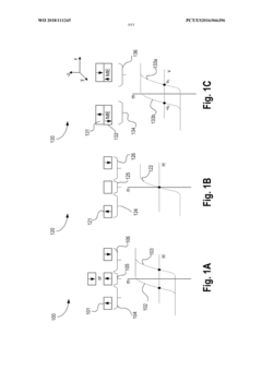
Spin orbit memory with multiferroic material
PatentActiveUS20190386202A1
Innovation
- A two-terminal memory bit-cell utilizing multiferroic materials, where the write electrode comprises heavy metals or antiferromagnetic materials with large spin-orbit torque to switch magnetization, decoupling read and write operations and enabling low-power, high-density memory storage.
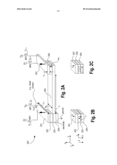
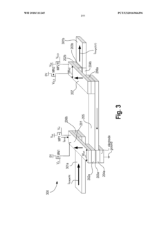
Perpendicular magnetoelectric spin orbit logic
PatentWO2018111245A1
Innovation
- The development of perpendicular Magnetoelectric Spin Orbit Logic (MESO) that utilizes the magnetoelectric effect to manipulate magnetization with an applied electric field, achieving spin-to-charge and charge-to-spin conversion through layers with the inverse Rashba-Bychkov effect and magnetoelectric switching, reducing switching energy and time while maintaining high speed operation.

Manufacturing Process Considerations and Integration Challenges
The manufacturing processes for both Spintronic and Phase-Change Memory (PCM) technologies present distinct challenges that significantly impact their commercial viability. Spintronic memories, particularly Magnetic Random Access Memory (MRAM), require precise deposition of multiple thin magnetic layers with thickness control at the atomic level. The manufacturing process involves complex physical vapor deposition (PVD) techniques and specialized equipment for creating the magnetic tunnel junction (MTJ) structures. Critical challenges include maintaining uniformity across large wafers and ensuring proper magnetic alignment during high-temperature back-end-of-line (BEOL) processing steps.
Integration of MRAM into existing CMOS processes requires careful consideration of thermal budgets, as excessive temperatures can degrade the magnetic properties of the MTJ. Additionally, etching processes for patterning MTJ stacks present significant difficulties due to the chemical resistance of magnetic materials and the risk of sidewall redeposition causing electrical shorts.
For PCM technologies, the manufacturing process centers around the deposition of chalcogenide materials, typically germanium-antimony-tellurium (GST) compounds. The primary challenge lies in controlling the crystallization properties of these materials across billions of memory cells. Uniform heating and cooling during programming operations demand precise thermal management solutions at the device level.
PCM integration faces challenges with material compatibility, as the phase-change materials may diffuse into surrounding structures during high-temperature processing. The electrode materials must also be carefully selected to provide sufficient current density for programming while maintaining thermal isolation between adjacent cells.
Both technologies face scaling challenges as dimensions decrease below 20nm. For MRAM, maintaining thermal stability of smaller magnetic domains becomes increasingly difficult, requiring innovations in materials and structure. PCM faces challenges with reduced programming volume leading to decreased signal margins and potential reliability issues.
From a manufacturing equipment perspective, MRAM requires specialized deposition and annealing tools not commonly found in standard semiconductor fabs, increasing capital expenditure requirements. PCM leverages more conventional semiconductor processing equipment but demands tight process control for the phase-change materials.
Yield management represents another critical consideration, with defect sensitivity increasing as cell sizes decrease. MRAM is particularly vulnerable to defects in the tunnel barrier, while PCM yield can be affected by compositional variations in the chalcogenide material or electrode interface quality issues.
Energy Efficiency and Power Consumption Analysis
Energy efficiency represents a critical factor in the evaluation and implementation of emerging memory technologies, particularly when comparing Spintronic and Phase-Change Memories (PCM). The fundamental operating principles of these technologies directly impact their power consumption profiles, creating distinct advantages and limitations for various applications.
Spintronic memories, particularly Magnetic Random Access Memory (MRAM), demonstrate remarkable static power efficiency due to their non-volatile nature. When not actively switching states, these memories consume negligible standby power, making them ideal for energy-constrained applications. The writing process in MRAM, however, presents energy challenges. Spin-Transfer Torque MRAM (STT-MRAM) requires significant current density to flip magnetic states, resulting in write operations that typically consume between 0.1-1 pJ per bit.
Phase-Change Memories operate on a different principle, utilizing resistive heating to transition between amorphous and crystalline states. This phase-change mechanism inherently demands substantial energy during write operations, with typical values ranging from 10-100 pJ per bit—significantly higher than MRAM counterparts. The thermal nature of PCM operations creates inherent inefficiencies as heat dissipation represents energy loss in the system.
Recent advancements have narrowed this efficiency gap. The development of voltage-controlled magnetic anisotropy in spintronic devices has reduced write energy requirements by up to 80% in experimental prototypes. Similarly, interface engineering in PCM has improved thermal efficiency, reducing write energy by approximately 40% in advanced implementations.
From a system-level perspective, the energy implications extend beyond individual cell operations. MRAM's faster write speeds (10-30ns) compared to PCM (50-500ns) translate to shorter active power windows, further enhancing overall system efficiency. Additionally, MRAM's superior endurance reduces the energy overhead associated with error correction and data refreshing operations that PCM systems often require.
Temperature sensitivity presents another dimension in the energy analysis. PCM exhibits increased leakage current at elevated temperatures, potentially compromising data retention without additional power-consuming refresh operations. Conversely, spintronic memories maintain relatively stable performance across wider temperature ranges, reducing the need for temperature compensation mechanisms that would otherwise consume additional power.
As scaling continues, the energy efficiency advantage increasingly favors spintronic solutions, particularly for edge computing and IoT applications where power constraints are paramount. However, PCM retains advantages in high-density storage applications where write operations are less frequent and the superior density-to-power ratio becomes the determining factor.
Unlock deeper insights with Patsnap Eureka Quick Research — get a full tech report to explore trends and direct your research. Try now!
Generate Your Research Report Instantly with AI Agent
Supercharge your innovation with Patsnap Eureka AI Agent Platform!