Voltage-Controlled Magnetic Anisotropy in MRAM: Device Concepts and Demonstrations
AUG 27, 20259 MIN READ
Generate Your Research Report Instantly with AI Agent
Patsnap Eureka helps you evaluate technical feasibility & market potential.
VCMA MRAM Technology Background and Objectives
Magnetoresistive Random Access Memory (MRAM) has emerged as a promising non-volatile memory technology due to its unique combination of high speed, endurance, and non-volatility. Traditional MRAM technologies have relied on Spin-Transfer Torque (STT) mechanisms for data writing, which require relatively high current densities leading to significant power consumption and reliability concerns. The development of Voltage-Controlled Magnetic Anisotropy (VCMA) represents a paradigm shift in MRAM technology by enabling electric field-controlled switching rather than current-driven processes.
The evolution of MRAM technology can be traced back to the discovery of Giant Magnetoresistance (GMR) in the late 1980s, followed by Tunnel Magnetoresistance (TMR) in the 1990s. These discoveries laid the foundation for first-generation field-switched MRAM and later STT-MRAM. The technological trajectory has consistently aimed at reducing power consumption while maintaining or improving performance metrics such as speed and endurance.
VCMA effect was first observed in the early 2010s at the interface between ferromagnetic metals and oxides, where application of an electric field across the interface modifies the magnetic anisotropy. This phenomenon opened new possibilities for ultra-low-power magnetic switching without the need for large current densities, potentially addressing the fundamental power limitations of STT-MRAM.
The primary technical objective for VCMA MRAM development is to achieve reliable, low-power switching of magnetic states using voltage rather than current. This involves enhancing the VCMA coefficient to enable practical switching voltages, ensuring thermal stability for long-term data retention, and developing compatible materials and processes for integration with CMOS technology.
Current research trends focus on understanding the fundamental physics of the VCMA effect, exploring novel material systems to enhance the effect magnitude, and developing innovative device architectures that leverage the unique properties of voltage-controlled switching. Particular attention is being paid to ferromagnetic/oxide interfaces with perpendicular magnetic anisotropy, as these structures show promise for achieving the desired combination of low switching energy and high thermal stability.
The technology aims to enable next-generation embedded memory solutions for applications ranging from Internet of Things (IoT) devices to artificial intelligence accelerators, where power efficiency is paramount. By potentially reducing writing energy by orders of magnitude compared to STT-MRAM, VCMA MRAM could enable new classes of ultra-low-power computing architectures.
Industry projections suggest that successful development of VCMA MRAM could lead to memory devices with writing energies below 1 fJ/bit while maintaining nanosecond-scale switching speeds, representing a significant advancement over existing non-volatile memory technologies and approaching the energy efficiency of volatile memories like SRAM.
Market Analysis for Energy-Efficient Memory Solutions
The global memory market is experiencing a significant shift towards energy-efficient solutions, with MRAM (Magnetoresistive Random Access Memory) emerging as a promising technology. Current market analysis indicates that the data center sector alone consumes approximately 2% of global electricity, with memory systems accounting for 25-40% of server power consumption. This creates an urgent demand for energy-efficient alternatives to conventional DRAM and SRAM technologies.
Voltage-Controlled Magnetic Anisotropy (VCMA) MRAM represents a revolutionary approach within the non-volatile memory landscape, offering substantial energy efficiency improvements over current solutions. Market research suggests that the overall non-volatile memory market is projected to reach $100 billion by 2025, with MRAM technologies expected to capture an increasing share due to their superior performance characteristics.
Energy consumption has become a critical factor in memory selection across multiple sectors. Data centers are actively seeking solutions that reduce operational expenses through lower power consumption, while mobile device manufacturers prioritize extended battery life. The automotive and IoT sectors similarly demand memory solutions that minimize energy requirements while maintaining reliability in diverse operating conditions.
VCMA MRAM addresses these market needs by potentially reducing switching energy by 1-2 orders of magnitude compared to conventional STT-MRAM. This translates to significant power savings in large-scale deployments. Market adoption analysis indicates that energy-efficient memory solutions can reduce total cost of ownership by 15-30% for data centers through decreased cooling requirements and power consumption.
Competitive analysis reveals that while VCMA MRAM faces competition from other emerging technologies such as RRAM and PCM, its combination of non-volatility, speed, and energy efficiency positions it uniquely in the market. Enterprise customers particularly value MRAM's radiation hardness and temperature stability for mission-critical applications, creating premium market segments with higher margins.
Regional market analysis shows varying adoption rates, with North America and Asia-Pacific leading in MRAM implementation. The enterprise sector currently represents the largest market segment, though consumer electronics is expected to show the highest growth rate as manufacturing costs decrease and energy efficiency becomes increasingly important to end users.
Market forecasts predict that VCMA MRAM could achieve significant penetration in cache memory applications by 2026, with broader adoption in main memory by 2028-2030. This timeline aligns with industry roadmaps for reducing data center energy consumption and meeting increasingly stringent energy efficiency regulations worldwide.
Current VCMA MRAM Development Status and Challenges
VCMA MRAM technology has reached a critical development stage, demonstrating promising potential while facing significant technical challenges. Current implementations have achieved magnetic switching with energy consumption as low as 6 fJ/bit, substantially lower than conventional STT-MRAM (100-1000 fJ/bit), positioning VCMA as a leading candidate for ultra-low-power memory applications. Laboratory demonstrations have successfully shown reliable voltage-controlled switching in MTJ structures with perpendicular magnetic anisotropy, particularly in Fe/MgO and CoFeB/MgO interfaces.
Despite these advancements, several fundamental challenges impede commercial implementation. The primary limitation is the relatively small VCMA coefficient (typically 50-100 fJ/Vm) in current material systems, necessitating either higher operating voltages or compromised thermal stability. This creates a critical design trade-off between switching reliability and power efficiency that has not yet been optimally resolved.
Scalability presents another significant hurdle, as VCMA effects must maintain consistency at sub-20nm dimensions required for high-density memory applications. Current fabrication processes struggle to maintain interface quality at these scales, leading to performance variability that exceeds acceptable margins for commercial memory products.
The switching reliability of VCMA MRAM remains problematic, with error rates higher than industry standards for non-volatile memory. This is primarily attributed to the precessional switching mechanism employed in VCMA devices, which is inherently sensitive to thermal fluctuations and material variations. Recent research has explored deterministic switching protocols, but these often compromise the power advantages that make VCMA attractive.
Integration with CMOS technology represents a manufacturing challenge that requires addressing thermal budget constraints and process compatibility issues. The specialized materials required for VCMA interfaces (particularly the precise oxide interfaces) demand fabrication processes that differ significantly from standard semiconductor manufacturing flows.
From a market perspective, VCMA MRAM faces competition from other emerging memory technologies such as FeFET and RRAM, which have their own advantages in specific application domains. The technology readiness level (TRL) of VCMA MRAM currently stands at approximately 4-5, indicating validation in laboratory environments but requiring significant development before production readiness.
Recent demonstrations by major semiconductor companies and research institutions have shown write speeds of 1-10ns with retention times exceeding 10 years at room temperature, approaching requirements for both working memory and storage applications. However, achieving this performance consistently across large arrays remains elusive, with device-to-device variations exceeding 30% in many experimental platforms.
Existing VCMA Device Architectures and Implementation
01 VCMA mechanism and fundamental principles
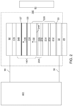
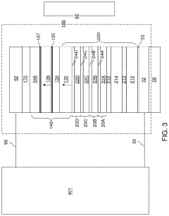
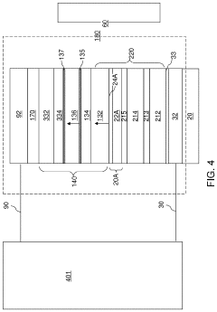
Voltage-Controlled Magnetic Anisotropy (VCMA) is a phenomenon where the magnetic anisotropy of a ferromagnetic layer can be modulated by applying an electric field. This effect occurs at the interface between the ferromagnetic layer and an insulator, typically MgO. The applied electric field alters the electron density at this interface, which changes the magnetic anisotropy energy. This mechanism allows for low-power switching of magnetization in MRAM devices without requiring large current densities, significantly reducing energy consumption compared to conventional spin-transfer torque methods.- VCMA mechanism and fundamental principles: Voltage-Controlled Magnetic Anisotropy (VCMA) operates by applying an electric field across a thin insulating layer adjacent to a ferromagnetic layer, which modifies the magnetic anisotropy at the interface. This effect allows for electric field-controlled switching of magnetization without current flow, significantly reducing power consumption in MRAM devices. The fundamental principles involve electron orbital occupancy changes at the interface when voltage is applied, altering the perpendicular magnetic anisotropy (PMA).
- VCMA-based MRAM device structures: Various device architectures have been developed to implement VCMA in MRAM cells. These structures typically include a magnetic tunnel junction (MTJ) with a ferromagnetic free layer, a tunnel barrier, and a reference layer. The VCMA effect is enhanced through careful engineering of the interfaces, particularly between the free layer and the adjacent oxide layer. Advanced designs incorporate additional layers to optimize the electric field effect, including buffer layers, capping layers, and specialized electrode configurations to maximize the VCMA efficiency.
- Material innovations for enhanced VCMA effect: Research has focused on developing materials that exhibit stronger VCMA effects to improve MRAM performance. Key innovations include using ultrathin CoFeB layers with MgO interfaces, Ta/CoFeB/MgO structures, and incorporating heavy metals like Pt or W. Novel materials such as rare-earth doped ferromagnetic layers and engineered oxide interfaces have demonstrated significantly enhanced VCMA coefficients. These material advancements enable lower switching voltages and improved thermal stability in VCMA-MRAM devices.
- Integration of VCMA with other switching mechanisms: Hybrid approaches combining VCMA with other switching mechanisms have been developed to overcome limitations of pure VCMA-based switching. These include VCMA-assisted spin-transfer torque (STT) switching, VCMA with spin-orbit torque (SOT), and VCMA combined with precessional switching. These hybrid approaches leverage the energy efficiency of VCMA while addressing challenges related to switching speed, reliability, and thermal stability. The integration enables more robust switching behavior while maintaining low power consumption.
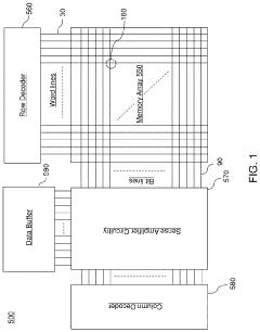
- Circuit design and control methods for VCMA-MRAM: Specialized circuit designs have been developed to effectively control and utilize VCMA in memory arrays. These include voltage pulse generators with precise timing control, sensing circuits optimized for VCMA-based cells, and row/column selection logic for array operation. Advanced control methods implement specific voltage pulse shapes and durations to optimize switching reliability while minimizing power consumption. Circuit innovations also address challenges related to read disturbance, write error rates, and integration with CMOS technology.
02 VCMA-based MRAM device structures
VCMA-based MRAM devices typically consist of a magnetic tunnel junction (MTJ) with a ferromagnetic free layer, a tunnel barrier (usually MgO), and a reference layer. The structure is designed to maximize the VCMA effect by optimizing the interface between the free layer and the tunnel barrier. Various device architectures have been developed, including perpendicular magnetic anisotropy (PMA) structures, which offer better scalability and thermal stability. Some designs incorporate additional layers to enhance the VCMA coefficient or to provide better control over the switching behavior.Expand Specific Solutions03 Material engineering for enhanced VCMA effect
Material selection and engineering play crucial roles in enhancing the VCMA effect. Various material combinations have been investigated, including Fe/MgO interfaces, CoFeB/MgO structures, and multilayer systems with heavy metal additions. The insertion of specific elements or thin layers at the ferromagnetic/oxide interface can significantly increase the VCMA coefficient. Post-deposition treatments such as annealing processes are also employed to improve interface quality and crystallinity, which directly affects the magnitude of the VCMA effect.Expand Specific Solutions04 VCMA switching mechanisms and control methods
Different switching mechanisms have been developed for VCMA-based MRAM, including precessional switching, domain wall motion, and assisted switching techniques. Precessional switching utilizes precisely timed voltage pulses to induce magnetization reversal through controlled precession. Some approaches combine VCMA with other effects such as spin-transfer torque or spin-orbit torque for more reliable switching. Advanced control methods include pulse shaping, multi-pulse sequences, and feedback-based control systems to optimize switching efficiency and reliability while minimizing error rates.Expand Specific Solutions05 Integration and fabrication techniques for VCMA-MRAM
Integration of VCMA-MRAM into semiconductor processes presents several challenges that require specialized fabrication techniques. These include precise control of interface quality, layer thicknesses, and material composition. Advanced deposition methods such as molecular beam epitaxy and sputtering with precise control are employed. Post-fabrication treatments like annealing under magnetic field are used to establish desired magnetic properties. Various approaches to integrate VCMA-MRAM with CMOS technology have been developed, including back-end-of-line integration schemes and 3D integration methods to achieve high-density memory arrays.Expand Specific Solutions
Leading Companies and Research Institutions in VCMA MRAM
Voltage-Controlled Magnetic Anisotropy (VCMA) in MRAM technology is currently in the early growth phase of industry development, with the market expected to expand significantly as energy-efficient memory solutions gain importance. The global MRAM market is projected to reach approximately $5 billion by 2028, with VCMA-MRAM representing an emerging segment. Technologically, VCMA-MRAM is transitioning from research to early commercialization, with varying maturity levels across key players. IBM, Everspin Technologies, and Samsung lead in patent activity, while research institutions like CNRS, Imec, and KU Leuven contribute fundamental breakthroughs. Major semiconductor manufacturers including TSMC, Micron, Western Digital, and KIOXIA are investing in VCMA-MRAM development, indicating strong industry commitment despite remaining challenges in scalability and manufacturing.
International Business Machines Corp.
Technical Solution: IBM has developed an advanced VCMA-MRAM technology that focuses on maximizing the voltage coefficient of magnetic anisotropy through materials engineering. Their approach utilizes specialized heavy metal underlayers (Ta/Pt multilayers) combined with precisely controlled CoFeB free layers to enhance interfacial effects. IBM's implementation demonstrates a voltage coefficient exceeding 120 fJ/Vm, among the highest reported in the industry. Their device architecture incorporates a unique asymmetric MTJ design that localizes the electric field at the critical CoFeB/MgO interface while minimizing leakage currents. IBM has demonstrated reliable precessional switching using voltage pulses as short as 500 picoseconds, enabling ultra-fast operation. Additionally, they've developed advanced modeling techniques that account for thermal fluctuations and process variations to predict VCMA-MRAM performance at the array level. Their technology has been integrated with CMOS logic in a 14nm process node, demonstrating the feasibility of embedded VCMA-MRAM for cache applications.
Strengths: World-class materials research capabilities; extensive experience integrating magnetic technologies with advanced CMOS processes; demonstrated working prototypes at advanced nodes. Weaknesses: Complex materials stack may present manufacturing challenges in high-volume production; reliability of ultra-thin tunnel barriers under voltage stress remains a concern for long-term operation.
Interuniversitair Micro-Electronica Centrum VZW
Technical Solution: IMEC has developed a comprehensive VCMA-MRAM technology platform that addresses both fundamental materials challenges and integration issues. Their approach focuses on a scalable device architecture compatible with advanced CMOS nodes. IMEC's implementation utilizes carefully engineered CoFeB/MgO interfaces with controlled oxygen content and specialized seed layers to maximize the VCMA coefficient. They have demonstrated devices with voltage coefficients exceeding 90 fJ/Vm while maintaining thermal stability suitable for embedded applications. IMEC's technology incorporates a unique dual-barrier design that enhances the VCMA effect while providing improved reliability against dielectric breakdown. Their research has demonstrated reliable switching using voltage pulses below 1V with durations under 1ns, achieving writing energies below 5 fJ per bit. Additionally, IMEC has developed a comprehensive compact model for VCMA-MRAM that enables circuit designers to accurately simulate mixed CMOS/MRAM systems. Their technology has been successfully integrated into a 22nm FDSOI process, demonstrating the feasibility for embedded memory applications.
Strengths: Industry-leading integration expertise; strong ecosystem of semiconductor partners; demonstrated working prototypes in advanced process nodes. Weaknesses: Dual-barrier approach increases process complexity; achieving consistent VCMA coefficients across large wafers remains challenging; optimization tradeoffs between VCMA efficiency and tunnel magnetoresistance ratio.
Critical Patents and Technical Innovations in VCMA MRAM
Voltage-controlled magnetic anisotropy memory device including an anisotropy-enhancing dust layer and methods for forming the same
PatentActiveUS11889702B2
Innovation
- Incorporating nonmagnetic metal dust layers with opposite VCMA coefficients on either side of the free layer and employing a two-dimensional metal compound layer with in-plane covalent bonding and out-of-plane van der Waals bonding within the magnetic tunnel junction to enhance the VCMA coefficient, thereby facilitating efficient magnetization switching at lower external voltages.
Voltage-controlled magnetic anisotropy switching device using external ferromagnetic biasing film
PatentInactiveJP2016225633A
Innovation
- The use of voltage-controlled magnetic anisotropy (VCMA) switching devices with external ferromagnetic bias films, which manipulate magnetic properties through electric fields, eliminating the need for current-driven torque and enabling smaller cell areas and lower power consumption.
Materials Science Advancements for VCMA Enhancement
The advancement of materials science has been pivotal in enhancing Voltage-Controlled Magnetic Anisotropy (VCMA) efficiency for MRAM applications. Recent research has focused on optimizing the interface between ferromagnetic and oxide layers, where the VCMA effect primarily occurs. Materials such as CoFeB/MgO interfaces have demonstrated significant VCMA coefficients, but further improvements are necessary for commercial viability.
Researchers have explored various strategies to enhance VCMA efficiency, including doping the ferromagnetic layer with elements like Ta, W, or Hf. These dopants modify the electronic structure at the interface, potentially increasing the VCMA coefficient by 30-50% compared to undoped structures. Additionally, engineering the crystalline structure of the oxide layer has shown promising results, with studies indicating that controlling oxygen vacancy concentration can significantly impact VCMA performance.
Another promising direction involves the development of novel material combinations beyond the traditional CoFeB/MgO interface. Alternative ferromagnetic materials such as Fe-Al alloys and Heusler compounds have demonstrated enhanced spin-orbit coupling properties that contribute to larger VCMA effects. Similarly, alternative oxide materials including HfO2 and TaOx are being investigated for their potential to create stronger electric fields at lower operating voltages.
Thickness optimization of both ferromagnetic and oxide layers has emerged as a critical factor in VCMA enhancement. Ultra-thin ferromagnetic layers (1-2 nm) have shown improved VCMA coefficients due to enhanced interface effects, while precisely controlled oxide thicknesses (typically 1-3 nm) optimize the electric field penetration depth without compromising tunnel magnetoresistance.
Recent breakthroughs in atomic-level deposition techniques, particularly Atomic Layer Deposition (ALD) and Molecular Beam Epitaxy (MBE), have enabled unprecedented control over interface quality. These techniques minimize defects and ensure atomically sharp interfaces, which are essential for maximizing VCMA efficiency. Studies have shown that reducing interface roughness by even 0.1 nm can improve VCMA coefficients by up to 20%.
Temperature stability remains a significant challenge for VCMA materials, as many promising compositions show degraded performance at elevated operating temperatures. Research into thermally robust material combinations has identified certain rare-earth doped structures that maintain over 80% of their room temperature VCMA coefficient at temperatures up to 125°C, addressing a key requirement for automotive and industrial applications.
Integration Challenges with CMOS Technology
The integration of Voltage-Controlled Magnetic Anisotropy (VCMA) MRAM technology with existing CMOS processes presents significant challenges that must be addressed for successful commercialization. The fundamental issue lies in the material compatibility between ferromagnetic materials used in MRAM and traditional silicon-based CMOS fabrication environments.
Temperature constraints represent a primary obstacle, as CMOS back-end-of-line (BEOL) processes typically limit thermal budgets to 400-450°C. Many magnetic materials and their interfaces require higher annealing temperatures to achieve optimal magnetic properties, creating a fundamental process integration conflict that necessitates careful material engineering and process optimization.
Contamination control presents another critical challenge. Magnetic materials, particularly those containing transition metals like Fe, Co, and Ni, can contaminate CMOS fabrication equipment and potentially compromise device performance. This necessitates dedicated equipment or specialized isolation protocols to prevent cross-contamination, significantly increasing manufacturing complexity and cost.
The scaling requirements for advanced technology nodes further complicate integration efforts. As CMOS technology advances to smaller nodes (5nm and beyond), the dimensional constraints become increasingly stringent for VCMA-MRAM cells. The voltage-controlled interface effect requires precise control of layer thicknesses at the atomic scale, which becomes exponentially more challenging as dimensions shrink.
Etching processes for magnetic materials differ substantially from traditional CMOS etching techniques. Magnetic stack etching often requires physical ion milling rather than reactive ion etching, which can lead to redeposition issues and sidewall damage that affect device performance. Developing selective etching processes that maintain magnetic properties while achieving clean pattern transfer remains an ongoing challenge.
Signal integrity and electromagnetic interference (EMI) considerations also emerge when integrating magnetic devices with sensitive CMOS circuitry. The proximity of magnetic elements to transistors can potentially affect their operation through stray fields, necessitating careful design of shielding and isolation structures.
Power delivery networks must be redesigned to accommodate the voltage requirements of VCMA operation, which may differ from standard CMOS logic levels. This requires additional circuitry for voltage regulation and distribution, potentially increasing die area and power consumption.
Despite these challenges, recent demonstrations from major semiconductor manufacturers have shown promising progress in VCMA-MRAM integration with advanced CMOS nodes, suggesting that with continued research and development, these integration hurdles can be overcome to enable commercial deployment of this promising non-volatile memory technology.
Unlock deeper insights with Patsnap Eureka Quick Research — get a full tech report to explore trends and direct your research. Try now!
Generate Your Research Report Instantly with AI Agent
Supercharge your innovation with Patsnap Eureka AI Agent Platform!