

How to Integrate Spintronics into CMOS: Process Flow, Compatibility and Yield
AUG 27, 20259 MIN READ
Generate Your Research Report Instantly with AI Agent
Patsnap Eureka helps you evaluate technical feasibility & market potential.
Spintronics-CMOS Integration Background and Objectives
Spintronics, a field that exploits the intrinsic spin of electrons in addition to their charge, has emerged as a promising technology for next-generation computing systems. The evolution of spintronics began in the late 1980s with the discovery of giant magnetoresistance (GMR), which led to the 2007 Nobel Prize in Physics. Since then, the field has progressed through various milestones including tunnel magnetoresistance (TMR), spin-transfer torque (STT), and more recently, spin-orbit torque (SOT) technologies.
The integration of spintronics with conventional CMOS technology represents a critical frontier in semiconductor development, offering potential solutions to the scaling limitations faced by traditional silicon-based electronics. As Moore's Law approaches its physical limits, the semiconductor industry is actively seeking alternative computing paradigms that can provide enhanced performance while reducing power consumption.
The technical objectives for spintronics-CMOS integration are multifaceted. Primary goals include developing reliable fabrication processes that maintain CMOS compatibility, achieving high yield rates comparable to standard CMOS processes, and ensuring thermal budget compatibility between spintronic elements and CMOS components. Additionally, researchers aim to minimize process contamination risks while maximizing the performance benefits of hybrid systems.
Historical attempts at integration have faced significant challenges, particularly in terms of material compatibility and process temperature constraints. Early approaches often required substantial modifications to standard CMOS processes, limiting commercial viability. However, recent advances in materials science and fabrication techniques have opened new pathways for more seamless integration.
The technology trend clearly points toward a hybrid approach where spintronic devices complement rather than replace CMOS functionality. This complementary strategy leverages the strengths of both technologies: CMOS for logic operations and spintronics for non-volatile memory, sensing applications, and potentially novel computing paradigms such as neuromorphic systems.
Current research focuses on developing back-end-of-line (BEOL) integration schemes that allow spintronic elements to be incorporated after the temperature-sensitive CMOS front-end processes are completed. This approach minimizes thermal impact on CMOS components while enabling the addition of spintronic functionality.
Looking forward, the field is moving toward more sophisticated integration strategies that may eventually enable true co-design of CMOS and spintronic components from the ground up, potentially revolutionizing computing architecture. The ultimate technical goal remains the development of a standardized, commercially viable process flow that maintains high yield while fully exploiting the unique advantages of spintronic technology.
Market Analysis for Hybrid Spintronics-CMOS Solutions
The global market for hybrid spintronics-CMOS solutions is experiencing significant growth, driven by increasing demands for energy-efficient computing and data storage technologies. Current market valuations indicate that the spintronics market reached approximately 12.5 billion USD in 2023, with projections suggesting a compound annual growth rate (CAGR) of 34% through 2030, potentially reaching 95 billion USD by the end of the decade.
The demand for hybrid spintronics-CMOS solutions is primarily concentrated in four key sectors. Data storage represents the largest market segment, accounting for nearly 45% of current applications. The integration of spintronics with CMOS technology offers substantial improvements in storage density and power efficiency compared to conventional technologies, addressing critical challenges in data centers.
Computing hardware constitutes the second-largest market segment at 30%, where hybrid solutions promise significant advancements in non-volatile computing architectures. This segment is expected to grow at the fastest rate due to increasing interest in neuromorphic computing and artificial intelligence applications that can leverage the unique properties of spintronic devices.
Telecommunications equipment manufacturers represent 15% of the market, with particular interest in high-frequency applications where spin-based devices offer superior performance characteristics. The remaining 10% is distributed across various sectors including automotive, aerospace, and healthcare, where specialized applications benefit from the radiation hardness and temperature stability of spintronic components.
Geographically, North America leads the market with 38% share, followed by Asia-Pacific at 35%, Europe at 22%, and other regions at 5%. However, the Asia-Pacific region is expected to demonstrate the highest growth rate over the next five years, driven by substantial investments in semiconductor manufacturing infrastructure in countries like Taiwan, South Korea, and China.
Market adoption faces several challenges, including cost barriers associated with manufacturing integration, technical complexity of hybrid processes, and competition from alternative emerging technologies. Current production costs for hybrid spintronics-CMOS devices remain 2.5 to 3 times higher than conventional CMOS, primarily due to yield issues and specialized equipment requirements.
Industry analysts identify three critical market inflection points that could accelerate adoption: achievement of manufacturing yields above 85% for hybrid processes, demonstration of 50% or greater power efficiency improvements in commercial applications, and successful integration with advanced CMOS nodes below 5nm. Recent industry developments suggest the first of these milestones could be reached within 18-24 months, potentially triggering more widespread commercial adoption.
Technical Challenges in Spintronics-CMOS Integration
The integration of spintronics with CMOS technology presents significant technical challenges that must be overcome to achieve commercially viable devices. Temperature compatibility remains one of the most critical issues, as many spintronic materials and processes require high temperatures that can damage or alter the properties of existing CMOS structures. Conversely, some spintronic materials lose their desirable magnetic properties when subjected to the high temperatures used in standard CMOS processing.
Material interface engineering presents another substantial hurdle. The junction between spintronic materials and silicon often creates unwanted interfacial layers or diffusion problems that can degrade device performance. Achieving atomically clean interfaces with minimal defects requires precise deposition techniques and potentially new barrier materials specifically designed for spintronic-CMOS integration.
Etching and patterning spintronic materials introduce unique challenges not encountered in traditional CMOS fabrication. Many magnetic materials are difficult to etch using conventional plasma processes without causing sidewall damage or redeposition issues that can compromise magnetic properties. The development of selective etching techniques that preserve magnetic characteristics while achieving nanoscale precision remains an active research area.
Contamination control represents a significant concern in integrated facilities. Magnetic materials can potentially contaminate standard CMOS equipment, necessitating dedicated tools or innovative isolation strategies. This separation increases manufacturing complexity and costs, creating barriers to widespread adoption.
Scaling spintronic devices to match the dimensions of advanced CMOS nodes (currently at 5nm and below) presents fundamental physical limitations. As dimensions shrink, maintaining thermal stability and sufficient signal-to-noise ratios becomes increasingly difficult for magnetic elements, potentially limiting the scalability of integrated spintronic-CMOS systems.
Reliability and yield management introduce additional complexities. Spintronic devices may exhibit different failure mechanisms compared to conventional CMOS, requiring new testing methodologies and reliability models. The interaction between magnetic elements and traditional semiconductor components can create unique aging and wear-out mechanisms that must be characterized and mitigated.
Process variability affects spintronic devices differently than CMOS components. Variations in magnetic layer thickness, composition, or interface quality can dramatically impact device performance, necessitating tighter process controls and potentially new in-line metrology techniques specifically designed for magnetic properties.
Design tool integration remains underdeveloped, with most electronic design automation (EDA) platforms lacking robust models for spintronic devices. This gap complicates the creation of hybrid circuits and limits the ability of designers to fully leverage the unique capabilities of spintronic-CMOS integration.
Current Process Flow Solutions for Hybrid Integration
01 Integration of spintronic devices with CMOS technology
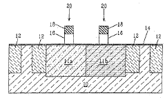
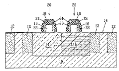
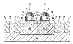
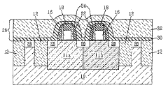
Spintronic devices can be integrated with conventional CMOS technology to create hybrid systems that leverage the advantages of both technologies. This integration involves fabricating spintronic components such as magnetic tunnel junctions (MTJs) alongside CMOS transistors on the same chip. The process requires careful consideration of material compatibility and process temperatures to ensure that the spintronic elements do not degrade during CMOS processing steps. Such integration enables the development of non-volatile memory and logic circuits with improved performance and energy efficiency.- Integration of spintronic devices with CMOS technology: Spintronic devices can be integrated with conventional CMOS technology to create hybrid systems that leverage the advantages of both technologies. This integration involves fabricating spintronic elements such as magnetic tunnel junctions (MTJs) alongside traditional CMOS components on the same chip. The process requires careful consideration of material compatibility, thermal budgets, and process sequences to ensure that the fabrication of spintronic elements does not degrade the performance of CMOS transistors and vice versa.
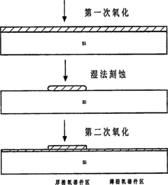
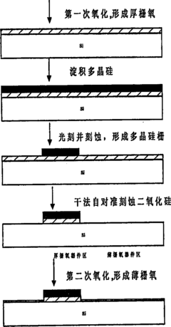
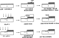
- Process flow compatibility challenges and solutions: Integrating spintronics with CMOS presents several process flow compatibility challenges. These include thermal budget constraints, as spintronic materials often require lower processing temperatures than standard CMOS processes. Solutions involve developing back-end-of-line integration approaches where spintronic devices are fabricated after the high-temperature CMOS front-end processes are completed. Additionally, specialized deposition techniques and etching processes have been developed to ensure the integrity of magnetic materials during integration.
- Yield improvement techniques for spintronic-CMOS integration: Improving yield in spintronic-CMOS integrated circuits requires addressing specific failure mechanisms unique to magnetic materials and interfaces. Techniques include optimizing deposition parameters for uniform magnetic layers, developing specialized etching processes that minimize damage to magnetic properties, implementing protective layers to prevent oxidation and contamination, and designing redundancy schemes to compensate for potential device failures. Advanced inspection and testing methodologies have also been developed to identify and mitigate yield-limiting factors specific to spintronic devices.
- Novel materials and structures for enhanced compatibility: Novel materials and device structures have been developed to enhance the compatibility between spintronic and CMOS technologies. These include buffer layers to improve adhesion and prevent interdiffusion, specialized barrier materials to isolate magnetic elements from CMOS components, and engineered magnetic stacks with improved thermal stability. Additionally, innovative device architectures have been designed to minimize the impact of stray magnetic fields on CMOS operation while maintaining the functionality of spintronic elements.
- Manufacturing and testing methodologies for integrated spintronic-CMOS devices: Specialized manufacturing and testing methodologies have been developed for integrated spintronic-CMOS devices. These include modified lithography processes to accommodate the unique requirements of magnetic materials, specialized etching techniques that preserve magnetic properties, and non-destructive testing methods for evaluating device performance. Additionally, design-for-manufacturing approaches have been implemented to enhance process margins and improve overall yield, including layout optimizations and process control strategies specific to spintronic-CMOS integration.
02 Process flow compatibility challenges and solutions
Integrating spintronics with CMOS presents significant process flow challenges due to different material requirements and thermal budgets. Solutions include back-end-of-line integration where spintronic devices are fabricated after the temperature-sensitive CMOS processes are completed, development of low-temperature deposition techniques for magnetic materials, and use of protective layers to shield spintronic elements during high-temperature steps. Advanced etching techniques and planarization methods are also employed to ensure proper interconnection between spintronic and CMOS components while maintaining the integrity of both technologies.Expand Specific Solutions03 Yield improvement techniques for spintronic-CMOS integration
Improving manufacturing yield in spintronic-CMOS integration involves several techniques including optimized deposition methods for uniform magnetic layers, precise control of interface quality between magnetic and non-magnetic materials, and development of robust etch processes that minimize damage to magnetic structures. Advanced testing methodologies specific to spintronic devices help identify defects early in the manufacturing process. Statistical process control and design for manufacturability approaches tailored to spintronic-CMOS hybrid circuits further enhance yield by addressing common failure mechanisms and process variations.Expand Specific Solutions04 Novel materials and structures for CMOS-compatible spintronics
Research into novel materials and device structures has enabled better compatibility between spintronics and CMOS technologies. These include development of perpendicular magnetic anisotropy materials that offer thermal stability at smaller dimensions, use of synthetic antiferromagnets to reduce stray magnetic fields that might interfere with CMOS operation, and exploration of alternative channel materials like graphene or topological insulators that can efficiently transport spin information. These innovations help address scaling challenges and improve the performance of integrated spintronic-CMOS systems.Expand Specific Solutions05 Testing and reliability assessment of integrated spintronic-CMOS devices
Specialized testing methodologies have been developed to assess the reliability and performance of integrated spintronic-CMOS devices. These include accelerated aging tests to evaluate the long-term stability of magnetic properties, measurement techniques for spin transfer efficiency, and characterization of read/write endurance in memory applications. Reliability models that account for unique failure mechanisms in spintronic devices, such as magnetic layer degradation and tunnel barrier breakdown, help predict device lifetime under various operating conditions. These testing approaches are essential for qualifying spintronic-CMOS technology for commercial applications.Expand Specific Solutions
Key Industry Players in Spintronics-CMOS Development
Spintronics integration into CMOS technology is currently in the early commercialization phase, with a growing market projected to reach significant scale as applications in memory and logic devices expand. The competitive landscape features established semiconductor giants like Intel, Samsung, and TSMC leading industrial implementation, while specialized players such as Infineon and GlobalFoundries are developing compatible process flows. Academic institutions including University of California and Peking University are contributing fundamental research to overcome key technical challenges. Technical maturity varies across applications, with MRAM technologies being more advanced than logic implementations, though yield optimization and material compatibility remain industry-wide challenges that all players are addressing through collaborative research initiatives and specialized fabrication techniques.
Intel Corp.
Technical Solution: Intel has developed a comprehensive approach to integrating spintronics into CMOS technology through their Magnetoresistive Random-Access Memory (MRAM) program. Their process flow involves a "back-end-of-line" (BEOL) integration strategy where magnetic tunnel junction (MTJ) elements are fabricated after the standard CMOS transistors. Intel's approach includes: (1) Deposition of multiple thin-film magnetic layers using Physical Vapor Deposition (PVD) techniques with precise thickness control (1-2nm precision); (2) Implementation of specialized etching processes that prevent re-deposition and maintain MTJ element integrity; (3) Development of thermal budget management techniques to ensure CMOS compatibility, as magnetic materials typically cannot withstand temperatures above 400°C; (4) Integration of specialized sensing circuits to detect the small resistance changes in MTJ devices. Intel has demonstrated successful integration of spin-transfer torque MRAM (STT-MRAM) with their 22nm FinFET CMOS technology, achieving bit yields exceeding 99.9% while maintaining CMOS performance.
Strengths: Industry-leading CMOS manufacturing expertise; established infrastructure for high-volume production; advanced materials engineering capabilities. Weaknesses: Higher manufacturing costs compared to conventional memory technologies; thermal stability challenges during integration; relatively lower storage density compared to NAND flash.
Taiwan Semiconductor Manufacturing Co., Ltd.
Technical Solution: TSMC has pioneered a modular integration approach for embedding spintronics into their advanced CMOS process nodes. Their technology focuses on embedding Spin-Transfer Torque Magnetic Random Access Memory (STT-MRAM) as embedded memory solutions. TSMC's process flow involves: (1) Completing standard CMOS front-end processing up to the contact level; (2) Depositing and patterning the magnetic tunnel junction (MTJ) stack between metal interconnect layers using specialized PVD systems with in-situ monitoring; (3) Implementing a unique ion beam etching process with sidewall protection to prevent shorting and material re-deposition; (4) Developing low-temperature dielectric deposition techniques compatible with magnetic materials; (5) Employing advanced Chemical-Mechanical Polishing (CMP) processes to ensure planarity after MTJ integration. TSMC has successfully demonstrated embedded MRAM technology at 22nm and 16nm nodes, with reported bit error rates below 0.1 ppm and endurance exceeding 10^6 cycles. Their process achieves over 95% yield for MRAM arrays while maintaining CMOS performance parameters.
Strengths: Advanced process node capabilities; extensive experience with heterogeneous integration; sophisticated quality control systems; established foundry services model for commercialization. Weaknesses: Higher manufacturing complexity increases production costs; thermal budget limitations restrict certain process options; specialized equipment requirements for magnetic material processing.
Critical Patents in Spintronics-CMOS Fabrication
Complementary metal oxide semiconductor (CMOS) structure
PatentInactiveJP2012054555A
Innovation
- A CMOS silicide metal gate integration scheme that uses a thick dielectric cap and selective etching to maintain uniform poly-Si gate thickness, followed by a salicide process to form metal silicide gates with consistent height and phase across the wafer.
Technique for preparing dual-gate oxygen on CMOS in high voltage compatible to standard technique of CMOS
PatentInactiveCN1873954A
Innovation
- Using a dry-wet etching method, the polysilicon gate is self-aligned to etch the thick gate oxide, and the step height of the polysilicon gate and the thin gate oxide area is relaxed through regular etching and sidewalls, combined with hydrofluoric acid bleaching. Protect the silicon surface and form a dual-gate oxide preparation process that is compatible with standard CMOS processes.
Material Compatibility and Interface Engineering
The integration of spintronics with CMOS technology presents significant challenges in material compatibility and interface engineering. Traditional CMOS processes utilize silicon-based materials, while spintronic devices often require magnetic materials such as ferromagnets, antiferromagnets, and heavy metals that are not standard in semiconductor fabrication. This fundamental difference creates compatibility issues that must be addressed through careful materials selection and interface design.
Material selection for spintronic-CMOS integration must consider thermal budget constraints, as many spintronic materials degrade at temperatures exceeding 400°C, well below the typical CMOS processing temperatures. Ferromagnetic materials like CoFeB, NiFe, and CoFe have emerged as promising candidates due to their relatively good thermal stability and strong magnetic properties. Additionally, tunnel barrier materials such as MgO have demonstrated excellent performance in maintaining high tunnel magnetoresistance while remaining compatible with CMOS back-end-of-line processes.
Interface engineering between spintronic and CMOS materials represents a critical challenge due to potential interdiffusion, oxidation, and formation of unwanted interfacial compounds. Research has shown that carefully designed buffer layers can significantly improve interface quality. For example, Ta, Ru, or W layers have been successfully employed to promote proper crystallization of magnetic layers while preventing diffusion of elements from the substrate. These buffer layers also help control the perpendicular magnetic anisotropy crucial for device performance.
Contamination control presents another significant challenge, as magnetic materials can potentially contaminate CMOS fabrication equipment. This necessitates dedicated tools or specialized process flows to maintain the integrity of both technologies. Recent advances in atomic layer deposition (ALD) techniques have shown promise in creating high-quality interfaces with minimal contamination risk, allowing for more precise control of layer thickness and composition at the atomic scale.
Surface roughness at interfaces significantly impacts spin transport efficiency and device performance. Techniques such as chemical-mechanical polishing (CMP) have been adapted to prepare ultrasmooth surfaces for spintronic device integration. Additionally, advanced deposition methods like ion-beam deposition and magnetron sputtering with optimized parameters have demonstrated the ability to create high-quality interfaces with minimal defects and interdiffusion.
Recent research has focused on developing novel material systems specifically designed for CMOS compatibility. Heusler alloys, for instance, offer high spin polarization while maintaining thermal stability compatible with back-end CMOS processes. Similarly, antiferromagnetic materials like IrMn and PtMn are gaining attention for their robustness against external magnetic fields and potential for high-density integration without magnetic crosstalk.
Scalability and Cost Analysis of Integration Methods
The economic viability of integrating spintronics into CMOS technology depends significantly on scalability and cost factors. Current integration methods vary considerably in their economic efficiency, with backend integration approaches generally offering better cost-performance ratios than frontend integration. This is primarily because backend processes can leverage existing CMOS fabrication infrastructure with minimal modifications, reducing capital expenditure requirements.
When analyzing the scalability of spintronic-CMOS integration, three critical dimensions emerge: wafer size compatibility, feature size scaling, and throughput capacity. Most advanced spintronic deposition techniques are currently optimized for 200mm wafers, while mainstream CMOS production has moved to 300mm platforms. This size mismatch creates significant yield challenges and increases per-unit costs when attempting large-scale production.
Feature size compatibility presents another substantial challenge. While CMOS technology has reached sub-10nm nodes, many spintronic devices still operate optimally at larger feature sizes (20-45nm). This dimensional mismatch necessitates complex integration strategies that often compromise either the spintronic device performance or the density advantages of advanced CMOS nodes.
Cost modeling reveals that material expenses constitute a significant portion of integration costs. Rare earth metals and specialized magnetic materials used in spintronic devices can cost 5-10 times more than standard CMOS materials. Additionally, the specialized deposition equipment for magnetic materials represents a substantial capital investment, with costs ranging from $5-15 million per tool, compared to $2-7 million for standard CMOS equipment.
Yield analysis indicates that current integration methods achieve approximately 60-75% yield for hybrid spintronic-CMOS devices, significantly lower than the 85-95% standard for pure CMOS processes. This yield gap translates directly to higher per-unit costs and represents one of the most significant economic barriers to widespread adoption.
Looking forward, economies of scale will play a crucial role in cost reduction. Current cost models suggest that spintronic-CMOS integration adds a 30-50% premium over standard CMOS fabrication. However, industry projections indicate this premium could decrease to 15-25% within five years as process optimization continues and equipment costs are amortized across larger production volumes.
Unlock deeper insights with Patsnap Eureka Quick Research — get a full tech report to explore trends and direct your research. Try now!
Generate Your Research Report Instantly with AI Agent
Supercharge your innovation with Patsnap Eureka AI Agent Platform!