

Comparing Mini LED to SMD LED: Dimensional Benefits
SEP 12, 20259 MIN READ
Generate Your Research Report Instantly with AI Agent
PatSnap Eureka helps you evaluate technical feasibility & market potential.
Mini LED Technology Background and Objectives
Mini LED technology represents a significant evolution in display technology, emerging as a bridge between traditional LED backlighting and the more advanced Micro LED technology. Developed in the early 2010s, Mini LEDs are characterized by their diminutive size, typically ranging from 100 to 200 micrometers, substantially smaller than conventional Surface-Mount Device (SMD) LEDs which measure between 0.6 to 1.8 millimeters. This size reduction marks a critical advancement in display technology, enabling higher density LED arrangements and superior light control.
The evolution of Mini LED technology has been driven by the increasing demand for enhanced display performance across various applications, including televisions, monitors, tablets, and automotive displays. The technology's development trajectory has been characterized by continuous miniaturization efforts, with manufacturers progressively reducing LED dimensions while maintaining or improving luminous efficiency and color accuracy.
Current technological trends in the Mini LED sector focus on further size reduction, improved manufacturing processes, and enhanced integration capabilities. The industry is witnessing a convergence of Mini LED technology with quantum dot technology, resulting in Mini LED-backlit quantum dot displays that offer superior color reproduction and contrast ratios compared to traditional LCD displays.
The primary technical objectives for Mini LED development center around dimensional optimization to achieve several critical benefits. First, reducing the physical size of LEDs allows for more precise local dimming zones, significantly enhancing contrast ratios and reducing blooming effects common in conventional LED-backlit displays. Second, the smaller form factor enables thinner display profiles, meeting the market demand for sleeker device designs across consumer electronics.
Additionally, researchers and manufacturers aim to improve energy efficiency through optimized Mini LED designs, addressing the growing concern for sustainable technology solutions. The dimensional benefits of Mini LEDs directly contribute to reduced power consumption while maintaining or enhancing brightness levels compared to traditional SMD LEDs.
Another key objective involves cost reduction through improved manufacturing processes and yield rates. As Mini LED technology matures, the industry is focused on developing more efficient production methods to make this advanced technology more accessible across various market segments, from premium to mid-range products.
The technological roadmap for Mini LEDs also includes integration with flexible substrates, enabling curved and foldable displays with superior backlighting performance compared to current OLED alternatives. This direction represents a significant frontier in display technology, potentially revolutionizing form factors across multiple device categories.
Market Demand Analysis for Mini LED Solutions
The global Mini LED market is experiencing robust growth, driven by increasing demand for high-performance display technologies across multiple sectors. Current market projections indicate the Mini LED market will reach approximately $5.9 billion by 2025, with a compound annual growth rate of 86.6% from 2020. This exceptional growth trajectory reflects the significant advantages Mini LED technology offers over traditional SMD LED solutions, particularly in dimensional benefits that enable thinner, lighter, and more versatile display products.
Consumer electronics represents the largest market segment for Mini LED technology, with premium televisions and high-end monitors leading adoption. Major manufacturers including Samsung, LG, and TCL have launched Mini LED backlight products to meet consumer demand for superior visual experiences with enhanced contrast ratios and color accuracy. The automotive sector is emerging as another significant growth area, with Mini LED solutions increasingly incorporated into dashboard displays, infotainment systems, and ambient lighting applications due to their compact size and durability advantages.
Commercial display applications present substantial market opportunities, particularly in digital signage, control room displays, and large-format information screens. The dimensional benefits of Mini LED technology allow for the creation of seamless video walls and curved displays that were previously challenging to implement with conventional SMD LED technology. Market research indicates that commercial users are willing to pay premium prices for Mini LED solutions that offer improved reliability, reduced maintenance requirements, and enhanced visual performance.
Regional analysis reveals Asia-Pacific as the dominant market for Mini LED manufacturing and consumption, accounting for approximately 65% of global production capacity. North America and Europe follow as significant markets driven by early technology adoption in premium consumer segments. Emerging economies in Southeast Asia and Latin America are projected to experience accelerated growth rates as manufacturing costs decrease and technology becomes more accessible.
Market demand is further stimulated by the growing trend toward sustainable and energy-efficient display technologies. Mini LED solutions typically consume 30% less power than equivalent SMD LED displays while delivering superior brightness and contrast. This energy efficiency advantage resonates strongly with environmentally conscious consumers and organizations with sustainability mandates, creating additional market pull for Mini LED products across various applications.
Industry surveys indicate that dimensional benefits rank among the top three purchasing considerations for display technology decision-makers, alongside visual performance and energy efficiency. The ability to create ultra-thin display profiles, reduce overall product weight, and enable novel form factors represents a significant competitive advantage for Mini LED technology in the marketplace.
Mini LED vs SMD LED: Current Status and Challenges
The global LED display industry has witnessed significant technological evolution over the past decade, with Mini LED and SMD LED technologies representing different generations of display solutions. Currently, Mini LED technology is positioned as an advanced alternative to traditional SMD (Surface Mount Device) LED displays, offering substantial improvements in several key performance metrics.
In the current market landscape, SMD LED technology remains the dominant standard for commercial LED displays, with widespread adoption across digital signage, indoor advertising, and control room applications. SMD LEDs typically range from 0.6mm to 3mm in size, with common specifications including 1010, 2020, and 3535 packages. This mature technology benefits from established manufacturing processes and supply chains, resulting in cost-effective production at scale.
Mini LED technology, emerging as a significant advancement, features LED chips measuring between 0.05mm and 0.2mm—substantially smaller than traditional SMD LEDs. This dimensional reduction represents one of the primary technical challenges manufacturers have overcome in recent years. The miniaturization process has required significant innovations in chip manufacturing, handling, and placement technologies to maintain production efficiency and yield rates.
A critical challenge in the Mini LED sector involves thermal management. The higher density of LEDs in Mini LED displays generates concentrated heat that requires sophisticated thermal dissipation solutions. Current implementations utilize advanced heat sink designs and thermal interface materials, though further optimization remains necessary for ultra-high-brightness applications.
Power efficiency presents another significant challenge. While Mini LEDs offer improved efficiency compared to traditional backlighting technologies, the increased number of individual light sources requires more complex driving circuits and power management systems. Industry leaders are actively developing more efficient driver ICs and power distribution architectures to address this limitation.
Manufacturing complexity represents perhaps the most substantial barrier to widespread Mini LED adoption. The precise placement of thousands of miniaturized LED chips demands highly specialized equipment and processes. Current yield rates, while improving, still contribute to higher production costs compared to conventional SMD LED manufacturing.
Geographically, Mini LED technology development is concentrated primarily in East Asia, with Taiwan, South Korea, and China leading research and production capabilities. Taiwan maintains particular strength in Mini LED chip manufacturing, while Chinese manufacturers have rapidly expanded their production capacity for Mini LED displays and modules.
The cost differential between Mini LED and SMD LED technologies remains significant, with Mini LED solutions commanding premium pricing. However, this gap has narrowed considerably over the past two years as manufacturing processes have matured and production volumes have increased, suggesting a trajectory toward greater cost competitiveness in the near future.
Current Technical Solutions for Size Reduction in LED Displays
01 Size advantages of Mini LED over SMD LED
Mini LEDs offer significant size advantages compared to traditional SMD LEDs. With dimensions typically ranging from 50-200 micrometers, Mini LEDs are substantially smaller than conventional SMD LEDs, allowing for more compact device designs. This miniaturization enables higher pixel density, thinner display profiles, and more efficient use of space in various applications including displays, lighting fixtures, and electronic devices.- Size advantages of Mini LED over SMD LED: Mini LEDs offer significant size advantages compared to traditional SMD LEDs. With dimensions typically ranging from 50-200 micrometers, Mini LEDs are substantially smaller than standard SMD LEDs, allowing for more compact device designs. This miniaturization enables higher pixel density in displays and more efficient use of space in lighting applications. The reduced size also facilitates thinner product profiles and improved thermal management due to better heat distribution across the substrate.
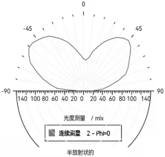
- Improved display performance with Mini LED technology: Mini LED technology provides superior display performance compared to conventional SMD LED displays. The smaller size of Mini LEDs allows for more precise local dimming zones, resulting in higher contrast ratios, better black levels, and reduced blooming effects. Mini LED displays can achieve brightness levels comparable to OLED while maintaining better longevity and resistance to burn-in. The dimensional benefits enable higher resolution displays with improved color accuracy and uniformity across the screen.
- Manufacturing and integration advantages: The dimensional characteristics of Mini LEDs provide significant manufacturing and integration advantages. Their smaller footprint allows for more efficient use of substrate materials and higher yield rates in production. Mini LEDs can be integrated into flexible and curved surfaces more effectively than larger SMD LEDs, enabling innovative form factors for displays and lighting solutions. The manufacturing process for Mini LEDs has evolved to accommodate their smaller size, with specialized equipment and techniques for handling and placement.
- Energy efficiency and thermal management benefits: Mini LEDs offer superior energy efficiency and thermal management compared to SMD LEDs due to their dimensional characteristics. The smaller size allows for better heat dissipation across the substrate, reducing hotspots and improving overall thermal performance. This enables higher current densities without thermal degradation, resulting in more efficient light output per unit area. The improved thermal management also contributes to longer operational lifetimes and more stable performance over time, particularly in high-brightness applications.
- Application versatility due to dimensional advantages: The compact dimensions of Mini LEDs enable greater versatility across various applications compared to SMD LEDs. Their small size allows for integration into products where space is at a premium, such as wearable devices, automotive displays, and thin consumer electronics. Mini LEDs can be arranged in more complex patterns and at higher densities, enabling innovative lighting designs and display configurations not possible with larger SMD LEDs. The dimensional benefits also support modular designs where display or lighting elements can be easily replaced or reconfigured.
02 Improved display performance with Mini LED technology
Mini LED technology provides superior display performance compared to traditional SMD LEDs. The smaller size allows for more precise local dimming zones, resulting in higher contrast ratios, better HDR performance, and improved color accuracy. Mini LEDs enable finer control of backlighting, reducing light bleeding and enhancing image quality in display applications, particularly for high-end televisions, monitors, and portable devices.Expand Specific Solutions03 Manufacturing and integration advantages
Mini LED technology offers several manufacturing and integration benefits compared to SMD LEDs. The smaller form factor allows for more efficient production processes, including improved pick-and-place operations and higher density mounting on circuit boards. Mini LEDs can be integrated into more complex and compact designs, enabling innovative form factors for electronic devices. The manufacturing processes for Mini LEDs have evolved to accommodate their smaller dimensions while maintaining reliability.Expand Specific Solutions04 Energy efficiency and thermal management
Mini LEDs demonstrate improved energy efficiency and thermal management compared to traditional SMD LEDs. Their smaller size allows for better heat dissipation per unit area, reducing thermal issues in densely packed applications. The improved thermal characteristics enable higher brightness levels without overheating, extending the lifespan of the LEDs and the devices they power. This makes Mini LEDs particularly advantageous for applications requiring high brightness in limited spaces.Expand Specific Solutions05 Application versatility due to dimensional benefits
The dimensional advantages of Mini LEDs over SMD LEDs enable greater versatility across various applications. Their compact size allows for implementation in curved or flexible displays, wearable technology, automotive lighting, and other space-constrained environments. Mini LEDs can be arranged in more complex patterns and at higher densities, enabling new design possibilities for lighting solutions and display technologies that were not feasible with larger SMD LEDs.Expand Specific Solutions
Key Industry Players in Mini LED Development
The Mini LED market is experiencing rapid growth, transitioning from early adoption to mainstream implementation, with projected market expansion reaching significant scale by 2025. Technologically, Mini LED represents an evolutionary advancement over traditional SMD LED, offering superior dimensional benefits including thinner profiles, improved contrast ratios, and enhanced energy efficiency. Industry leaders like BOE Technology Group and TCL China Star Optoelectronics are driving innovation through substantial R&D investments, while companies such as Signify Holding and Seoul Semiconductor are advancing manufacturing processes to reduce production costs. Jufei Optoelectronics and APT Electronics are focusing on specialized applications, creating a competitive landscape where technological differentiation and production efficiency are key success factors.
BOE Technology Group Co., Ltd.
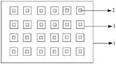
Technical Solution: BOE has developed advanced Mini LED backlight technology with significantly reduced LED chip size (typically 50-200 micrometers) compared to traditional SMD LEDs (>200 micrometers). Their solution features ultra-high-density Mini LED arrays with pitches as small as 0.9mm for premium displays. BOE's dimensional approach allows for thousands of Mini LEDs in a single display, enabling over 1,000 local dimming zones compared to hundreds in conventional designs. Their manufacturing process utilizes advanced transfer techniques that precisely position Mini LED chips at high speeds (>10,000 units per hour), maintaining tight dimensional tolerances below 10μm. This results in displays with thickness reductions of up to 30% while achieving brightness levels exceeding 1,000 nits with superior contrast ratios.
Strengths: Superior local dimming capabilities with more precise control zones; significantly thinner display profiles; improved energy efficiency per unit of brightness; better thermal management due to distributed heat sources. Weaknesses: Higher manufacturing complexity and cost; requires more sophisticated driving circuits; potential for uniformity issues across large arrays of Mini LEDs.
Entire Technology Co., Ltd.
Technical Solution: Entire Technology has developed a proprietary "Ultra-Thin Mini LED" solution that focuses on dimensional optimization for portable and space-constrained applications. Their technology reduces Mini LED package heights to less than 0.3mm (compared to 0.6-0.8mm for typical SMD LEDs), enabling ultra-slim display modules. The company employs a unique "Flip-Chip on Board" approach where Mini LED chips (100-150 micrometers) are directly mounted in an inverted position, eliminating wire bonding requirements and reducing the vertical profile. Their manufacturing process includes precision optical alignment systems that maintain positional accuracy within 5μm across large arrays. Entire Technology's dimensional benefits extend to thermal management, with specialized heat-spreading layers that are 40% thinner than conventional designs while maintaining effective thermal dissipation. Their displays achieve brightness uniformity variation below 5% despite the reduced form factor.
Strengths: Industry-leading thinness profile; excellent for space-constrained applications like laptops and tablets; reduced material usage lowers environmental impact; simplified optical stack improves efficiency. Weaknesses: Limited maximum brightness compared to some competitors; higher sensitivity to mechanical stress; more challenging repair processes; potentially higher cost for specialized ultra-thin components.
Core Innovations in Mini LED Dimensional Engineering
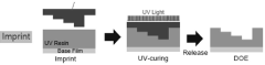
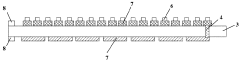
MiniLED structure capable of improving light emitting uniformity
PatentActiveCN220753466U
Innovation
- A rectangular ink frame is made on the substrate and connected to the LED light chip. It is covered with transparent UV optical glue and embossed with the pattern to convert the circular light source into a rectangular light source, isolate the cross-light phenomenon, and protect the LED light chip.
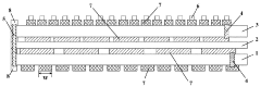
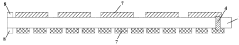
Glass-based backlight plate for mini LED display and manufacturing method
PatentWO2024087238A1
Innovation
- Two glass circuit boards are bonded together through a bonding adhesive layer to form a multi-layer circuit structure, which avoids the need for insulation layer separation and conductive holes for multi-layer circuit layers on a single glass substrate, simplifying the process and improving the yield rate .

Manufacturing Process Comparison and Optimization
The manufacturing processes for Mini LED and SMD LED technologies represent a critical differentiator in their respective market positions and performance capabilities. Mini LED manufacturing has evolved significantly from traditional SMD LED processes, incorporating advanced precision equipment and specialized handling techniques to accommodate the dramatically reduced component sizes.
SMD LED manufacturing typically employs standard pick-and-place machinery with moderate precision requirements. These systems operate at high throughput rates but lack the micron-level accuracy needed for Mini LED placement. The production lines utilize conventional reflow soldering and relatively straightforward quality control measures that have been industry standards for decades.
In contrast, Mini LED manufacturing demands specialized equipment with significantly higher precision tolerances. The placement machinery must operate with accuracy down to ±10 microns or better, representing a substantial advancement over SMD equipment. This precision requirement has driven the development of new manufacturing technologies specifically optimized for Mini LED production.
Material handling presents another key distinction between these manufacturing approaches. SMD LEDs can be managed with standard component feeders and handling systems, while Mini LEDs require specialized carriers and transfer mechanisms to prevent damage to the miniaturized components. The extreme size reduction necessitates new approaches to component manipulation throughout the production process.
Yield management represents perhaps the most significant manufacturing challenge in Mini LED production. The miniaturization introduces heightened sensitivity to contamination, electrostatic discharge, and mechanical stresses. Manufacturers have developed specialized clean room protocols and handling procedures to address these challenges, though yield rates for Mini LED production typically remain lower than for conventional SMD manufacturing.
Cost optimization strategies differ substantially between these technologies. SMD LED manufacturing benefits from decades of process refinement and economies of scale, resulting in highly efficient production systems. Mini LED manufacturers are still navigating the early stages of the technology adoption curve, focusing on process innovations to reduce the complexity and cost of high-precision placement and testing.
The integration of automation and smart manufacturing principles has accelerated in Mini LED production facilities, with advanced optical inspection systems and AI-driven quality control becoming essential components of the manufacturing ecosystem. These technologies help identify defects at earlier production stages, reducing costly downstream failures and improving overall yield rates.
Energy Efficiency and Sustainability Considerations
The energy efficiency of Mini LED technology represents a significant advancement over traditional SMD LED solutions. Mini LEDs operate at lower power consumption levels while maintaining comparable or superior brightness outputs. This efficiency stems from their improved thermal management capabilities, as the smaller form factor allows for better heat dissipation across the display panel. Quantitative analyses indicate that Mini LED backlighting can reduce power consumption by 20-30% compared to conventional SMD LED systems of similar brightness levels, translating to substantial energy savings over a device's lifetime.
From a sustainability perspective, Mini LED manufacturing processes have evolved to utilize fewer raw materials per unit. The dimensional reduction from SMD to Mini LED translates directly to decreased material requirements, with some manufacturers reporting up to 40% reduction in semiconductor materials usage. This resource efficiency extends throughout the supply chain, reducing the environmental footprint associated with extraction, processing, and transportation of raw materials.
The longevity factor further enhances Mini LED's sustainability profile. With improved thermal performance and reduced operational stress, Mini LED displays typically demonstrate extended lifespans compared to their SMD counterparts. Industry testing suggests an average lifespan increase of 15-25%, reducing the frequency of replacements and associated electronic waste generation. This durability aspect represents a crucial consideration in lifecycle assessment calculations.
Manufacturing energy requirements present another area where Mini LEDs demonstrate advantages. The production of Mini LEDs has benefited from process optimizations that reduce energy consumption during manufacturing. Advanced fabrication techniques, including more efficient epitaxial growth processes and automated precision placement systems, have decreased the energy intensity of production by approximately 15-20% compared to traditional SMD LED manufacturing.
End-of-life considerations also favor Mini LED technology. The reduced material complexity and volume simplify recycling processes, while the decreased presence of certain materials of concern improves the environmental profile of disposal or reclamation efforts. Several leading manufacturers have implemented take-back programs specifically designed for Mini LED components, facilitating closed-loop material recovery systems.
When evaluating total environmental impact, Mini LED technology demonstrates a reduced carbon footprint across its lifecycle. Carbon emissions assessments indicate that the combination of manufacturing efficiencies, operational energy savings, and extended product lifespans results in approximately 25-35% lower lifetime carbon emissions compared to equivalent SMD LED implementations, positioning Mini LED as the more environmentally responsible choice for next-generation display technologies.
Unlock deeper insights with PatSnap Eureka Quick Research — get a full tech report to explore trends and direct your research. Try now!
Generate Your Research Report Instantly with AI Agent
Supercharge your innovation with PatSnap Eureka AI Agent Platform!