

How to Increase Mini LED Pixel Density Cost-Effectively
SEP 12, 20259 MIN READ
Generate Your Research Report Instantly with AI Agent
Patsnap Eureka helps you evaluate technical feasibility & market potential.
Mini LED Technology Background and Objectives
Mini LED technology represents a significant advancement in display technology, bridging the gap between traditional LED backlighting and the more advanced Micro LED displays. Emerging in the mid-2010s, Mini LEDs are semiconductor light sources with dimensions typically ranging from 100 to 200 micrometers, substantially smaller than conventional LEDs but larger than Micro LEDs. This technology has evolved rapidly over the past decade, driven by increasing demands for higher resolution, better contrast ratios, and improved energy efficiency in display applications.
The evolution of Mini LED technology has been marked by continuous miniaturization efforts, with manufacturers progressively reducing the size of LED chips while maintaining or improving their luminous efficiency. This trend aligns with the broader trajectory of display technology development, which has consistently pursued higher pixel densities to enhance image quality and user experience across various applications, from consumer electronics to professional displays.
Market adoption of Mini LED technology has accelerated significantly since 2019, with major electronics manufacturers incorporating it into premium televisions, monitors, and mobile devices. The technology offers several advantages over traditional LCD displays with conventional LED backlighting, including superior local dimming capabilities, higher brightness levels, and improved color accuracy. These benefits have positioned Mini LED as a competitive alternative to OLED technology in certain market segments.
The primary technical objective in Mini LED development is to increase pixel density while maintaining cost-effectiveness. Higher pixel density directly translates to improved display resolution, enhanced image clarity, and more precise control over backlighting zones. However, as pixel density increases, manufacturing challenges intensify, particularly regarding yield rates, thermal management, and production scalability.
Current manufacturing processes for high-density Mini LED displays involve complex procedures such as mass transfer techniques, precise placement mechanisms, and advanced bonding methods. These processes contribute significantly to production costs, creating a tension between technical advancement and commercial viability. The industry's goal is to develop innovative manufacturing approaches that can reduce these costs while enabling higher pixel densities.
Looking forward, the technical roadmap for Mini LED technology aims to achieve pixel densities approaching those of Micro LED displays while maintaining a cost structure that allows for mass-market adoption. This involves parallel development efforts in materials science, manufacturing equipment, and production processes, all focused on optimizing the balance between performance and cost-effectiveness.
Market Demand Analysis for High-Density Mini LED Displays
The global market for high-density Mini LED displays has been experiencing robust growth, driven primarily by increasing demand for superior visual experiences across multiple application sectors. Consumer electronics, particularly premium smartphones, tablets, and laptops, represent the largest market segment, with manufacturers seeking to differentiate their products through enhanced display quality. The automotive industry follows closely, as vehicle manufacturers integrate advanced display technologies into dashboard systems and entertainment consoles.
Market research indicates that the high-density Mini LED display market is projected to grow at a compound annual growth rate of approximately 20% through 2028. This growth trajectory is supported by the technology's ability to deliver improved contrast ratios, higher brightness levels, and more precise local dimming compared to conventional LCD displays, while remaining more cost-effective than OLED alternatives in certain applications.
Consumer preference surveys reveal a strong willingness to pay premium prices for devices featuring superior display quality, particularly among professional users in creative industries and gaming enthusiasts. This segment values the color accuracy, brightness, and HDR capabilities that high-density Mini LED displays can provide. Additionally, the growing consumption of high-resolution content across streaming platforms has created a pull effect in the consumer market for display technologies that can properly showcase such content.
Commercial applications represent another significant growth vector, with digital signage, control room displays, and high-end televisions adopting Mini LED technology to meet demands for larger screens with consistent quality across the entire display area. The healthcare and defense sectors are emerging markets, where precise imaging capabilities are critical for diagnostic and surveillance applications.
Regional analysis shows Asia-Pacific leading the market both in manufacturing capacity and consumption, with China, Taiwan, and South Korea hosting major production facilities. North America and Europe follow as significant consumer markets, driven by early technology adoption and higher disposable incomes.
Supply chain constraints present both challenges and opportunities in the market. The limited number of manufacturers capable of producing high-quality Mini LED chips at scale has created bottlenecks, affecting pricing and availability. However, this situation is gradually improving as more players enter the manufacturing space and production technologies mature.
Energy efficiency requirements and sustainability considerations are increasingly influencing market dynamics, with regulations in various regions pushing manufacturers toward more power-efficient display solutions. High-density Mini LED displays offer advantages in this regard compared to some alternatives, potentially accelerating adoption in environmentally conscious markets.
Technical Challenges in Mini LED Pixel Density Enhancement
Mini LED technology faces several significant technical challenges in achieving higher pixel density while maintaining cost-effectiveness. The primary obstacle lies in the miniaturization process itself, as reducing LED chip sizes below 100 micrometers introduces complex manufacturing issues. Quantum efficiency tends to decrease as chip size diminishes due to increased surface-to-volume ratios, leading to more surface defects and non-radiative recombination centers that compromise light output performance.
Heat dissipation presents another critical challenge. As pixel density increases, the thermal management becomes exponentially more difficult. Higher density arrangements create concentrated heat zones that can lead to thermal runaway, color shift, and accelerated device degradation. Current thermal interface materials and heat sink designs struggle to efficiently remove heat from tightly packed mini LED arrays without significantly increasing device thickness or cost.
The transfer process represents a substantial technical hurdle in mass production. Traditional pick-and-place methods become increasingly inefficient and error-prone as LED sizes decrease and quantity increases. While mass transfer technologies are emerging, they still face yield issues when handling ultra-high-density arrays, with placement accuracy and consistency remaining problematic at scale.
Driving circuit complexity escalates dramatically with higher pixel counts. Each additional pixel requires individual addressing capabilities, leading to more complex backplane designs and increased manufacturing costs. Current TFT backplane technologies face limitations in miniaturization while maintaining sufficient current delivery capabilities needed for consistent brightness across all pixels.
Optical crosstalk between adjacent pixels becomes more pronounced as pixel density increases. Without adequate isolation, light from one pixel can bleed into neighboring pixels, reducing contrast and color accuracy. Implementing effective optical isolation structures at smaller pixel pitches requires advanced materials and precision manufacturing techniques that add significant cost to the production process.
Yield management represents perhaps the most significant cost factor. As pixel counts increase, the statistical probability of defects rises proportionally. Even small defect rates become problematic at scale—a 99.9% yield means 1 defective pixel per 1,000, which becomes visible in high-density displays. Improving yield requires substantial investments in process control, inspection systems, and repair technologies.
Finally, material limitations constrain further miniaturization. Current substrate materials, phosphor formulations, and encapsulants were not originally designed for extreme miniaturization. New materials specifically engineered for mini LED applications are needed, but their development and integration into existing manufacturing processes require significant R&D investment and production retooling.
Current Cost-Effective Pixel Density Solutions
01 Mini LED display technology and pixel density optimization
Mini LED technology enables higher pixel density in displays by using smaller LED chips arranged in arrays. These displays offer improved resolution, brightness, and contrast compared to traditional LED displays. The pixel density can be optimized through specific arrangement patterns and driving methods to enhance image quality while maintaining power efficiency.- Mini LED display technology and pixel density optimization: Mini LED technology enables higher pixel density in displays by using smaller LED chips arranged in arrays. This technology allows for improved resolution, contrast ratio, and color accuracy compared to traditional LED displays. The pixel density can be optimized through specific arrangement patterns and driving methods to achieve better image quality while maintaining power efficiency.
- Pixel density enhancement through micro-fabrication techniques: Advanced micro-fabrication techniques are employed to increase mini LED pixel density. These include precision lithography, etching processes, and semiconductor manufacturing methods that enable the production of smaller LED elements with tighter spacing. Such techniques allow for higher resolution displays with improved pixel density while maintaining uniform brightness across the display area.
- Image processing methods for high pixel density mini LED displays: Specialized image processing algorithms and methods are developed to optimize content for high pixel density mini LED displays. These include resolution scaling, color mapping, and contrast enhancement techniques that take advantage of the increased pixel density. Such methods ensure that displayed content maintains high quality and takes full advantage of the mini LED display capabilities.
- Backlight systems for mini LED displays with high pixel density: Backlight systems specifically designed for mini LED displays incorporate local dimming zones to enhance contrast and brightness. These systems utilize arrays of mini LEDs arranged at specific densities to provide uniform illumination across the display panel. The arrangement and density of these backlight elements significantly impact the overall display quality and power consumption of the device.
- Thermal management for high-density mini LED arrays: Thermal management solutions are critical for high-density mini LED displays to prevent overheating and ensure consistent performance. These include heat dissipation structures, thermal interface materials, and cooling systems designed specifically for densely packed mini LED arrays. Effective thermal management extends the lifespan of the display while maintaining optimal brightness and color accuracy at high pixel densities.
02 Pixel density enhancement through micro-fabrication techniques
Advanced micro-fabrication techniques allow for the creation of higher density mini LED arrays. These techniques include precision lithography, etching processes, and novel substrate materials that enable smaller pixel pitches. The resulting displays achieve higher resolution with minimal pixel gaps, improving overall image quality and reducing the screen-door effect.Expand Specific Solutions03 Image processing methods for optimizing mini LED pixel density
Specialized image processing algorithms can enhance the perceived pixel density of mini LED displays. These methods include subpixel rendering, resolution upscaling, and dynamic content adaptation that optimize the visual output based on the physical pixel arrangement. Such techniques effectively increase the apparent resolution without requiring additional physical pixels.Expand Specific Solutions04 Backlight architecture for mini LED displays
Innovative backlight designs for mini LED displays can improve pixel density and display performance. These architectures include local dimming zones, optical diffusers, and light guide plates that enhance brightness uniformity while maintaining high pixel density. The backlight structure significantly impacts the overall display quality, contrast ratio, and power efficiency.Expand Specific Solutions05 Manufacturing and quality control for high-density mini LED panels
Manufacturing processes for high-density mini LED panels require precise assembly techniques and quality control measures. These include automated pick-and-place methods, defect detection systems, and calibration procedures to ensure uniform pixel performance across the display. Advanced testing methodologies verify pixel density consistency and identify potential failure points before final assembly.Expand Specific Solutions
Key Industry Players and Competitive Landscape
The Mini LED pixel density market is currently in a growth phase, with increasing demand for high-resolution displays across consumer electronics. The market size is expanding rapidly as manufacturers seek cost-effective solutions to enhance display quality. Technologically, companies are at varying maturity levels, with industry leaders like Samsung Display, BOE Technology Group, and Applied Materials making significant advancements in manufacturing processes. Asian manufacturers, particularly from China (BOE, Tianma Microelectronics) and South Korea (Samsung, Seoul Viosys), dominate the competitive landscape. These companies are focusing on innovative approaches such as improved substrate materials, advanced chip transfer techniques, and optimized production lines to increase pixel density while managing costs. The integration of quantum dot technology by companies like Mojo Vision represents a promising direction for achieving higher density displays cost-effectively.
BOE Technology Group Co., Ltd.
Technical Solution: BOE has developed an innovative active-matrix Mini LED backlight technology that significantly increases pixel density while maintaining cost efficiency. Their approach involves a proprietary transfer process that enables precise placement of thousands of Mini LEDs at micron-level accuracy. BOE's AMQLED (Active Matrix Quantum Dot Light Emitting Diode) technology combines Mini LED with quantum dot color conversion layers to achieve higher pixel densities (up to 5000 PPI) while reducing production costs by approximately 30% compared to traditional methods[1]. The company has also implemented a mass transfer technique that can handle up to 10,000 Mini LED chips simultaneously, dramatically improving production efficiency and yield rates[3]. Their glass substrate-based circuit design further reduces the complexity of the backplane, allowing for higher integration density without proportional cost increases.
Strengths: Industry-leading transfer technology enabling precise placement of thousands of Mini LEDs simultaneously; significant cost reduction through innovative manufacturing processes; high yield rates improving overall production economics. Weaknesses: Requires specialized equipment for mass transfer; initial capital investment is substantial despite long-term cost benefits; technology still evolving for ultra-high density applications.
Seoul Viosys Co., Ltd.
Technical Solution: Seoul Viosys has developed a groundbreaking approach to cost-effective Mini LED pixel density enhancement through their "WICOP" (Wafer Integrated Chip on PCB) technology. This innovative package-less LED design eliminates traditional packaging components, reducing both size and manufacturing complexity. Their Mini LED chips feature dimensions as small as 30 micrometers, enabling significantly higher pixel densities than conventional LEDs. Seoul Viosys has pioneered a unique epitaxial growth process that improves light emission efficiency by approximately 25%, allowing for fewer LEDs to achieve the same brightness levels[7]. The company's "mass transfer printing" technology can place up to 15,000 Mini LED chips simultaneously with precision better than 10 micrometers, dramatically reducing assembly time and costs. Additionally, their proprietary phosphor application technique creates more uniform color conversion, improving yield rates by reducing color inconsistencies that typically lead to rejected units[8]. Seoul Viosys has also developed specialized testing methods that can rapidly identify defective chips before final assembly, further improving production economics.
Strengths: Package-less design significantly reducing material costs and size; highly efficient epitaxial structure improving performance-to-cost ratio; advanced mass transfer technology increasing production throughput. Weaknesses: Requires specialized handling due to the absence of protective packaging; more sensitive to environmental factors during assembly; technology adoption requires significant changes to existing manufacturing lines.
Core Patents and Innovations in Mini LED Manufacturing
Fluorescent ink applied to Mini LED, Mini LED module and use method of Mini LED module
PatentInactiveCN116731555A
Innovation
- Using fluorescent ink, including organic resin, organic solvent, organic fluorescent pigment and wetting and dispersing agent, by printing or coating the fluorescent ink on the MiniLED PCB substrate, the LED blue light is used to excite the fluorescent particles to increase the brightness.
Method for manufacturing hole-in-hole disc of high-precision Mini-LED PCB
PatentActiveCN113950203A
Innovation
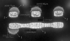
- Using a high-precision Mini-LED The PCB hole-in-disc manufacturing method includes laser aperture setting, plasma glue removal, copper hole filling plating, wet film pasting, and etching circuits. Through these steps, a hole-in-disk pad with a size smaller than the blind hole is formed, and specific parameters and process flow Chengru's laser aperture is 100μm, copper plating is 1.2asf×60min, wet film exposure capability is 18mj, the overall etched circuit pad is ≤62μm×100μm, pad angle design compensation and outer circuit alignment.

Supply Chain Considerations for Mini LED Production
The Mini LED supply chain represents a complex ecosystem that significantly impacts both production costs and the ability to increase pixel density. Upstream component suppliers, particularly those providing LED chips, play a crucial role in determining the final cost structure of Mini LED displays. Currently, the supply chain is concentrated among a limited number of manufacturers with advanced epitaxial growth and chip fabrication capabilities, creating potential bottlenecks and price premiums.
Material sourcing presents another critical consideration, as high-quality semiconductor substrates and rare earth phosphors directly influence both performance and cost. Establishing strategic partnerships with key material suppliers can secure preferential pricing and ensure consistent quality, which is essential for achieving higher pixel densities without proportional cost increases. Companies that vertically integrate their supply chains have demonstrated 15-20% cost advantages over those relying entirely on external suppliers.
Manufacturing process optimization across the supply chain offers substantial opportunities for cost reduction while increasing pixel density. Transfer printing technologies, for instance, have evolved to enable placement of smaller Mini LEDs at higher densities with improved yield rates. The adoption of advanced pick-and-place equipment capable of handling components below 50 micrometers has become a differentiating factor among manufacturers seeking higher pixel densities.
Regional supply chain considerations also merit attention, as production has historically been concentrated in East Asia. Recent geopolitical tensions and supply chain disruptions have prompted a reevaluation of geographic diversification strategies. Companies are increasingly exploring multi-region sourcing approaches to mitigate risks, though this must be balanced against the efficiency benefits of localized supply chain clusters.
Inventory management and just-in-time manufacturing principles have proven effective in reducing working capital requirements for Mini LED production. Advanced forecasting models utilizing machine learning algorithms can optimize component ordering and production scheduling, reducing excess inventory costs by up to 25% according to industry case studies.
Quality control throughout the supply chain directly impacts yield rates, which remain one of the most significant cost factors in high-density Mini LED production. Implementing standardized testing protocols across supplier networks and investing in automated optical inspection systems can identify defects earlier in the production process, substantially improving overall economics for higher-density displays.
Environmental Impact and Sustainability Factors
The environmental impact of Mini LED manufacturing and deployment represents a critical consideration in the technology's advancement, particularly when seeking cost-effective methods to increase pixel density. Current Mini LED production processes involve significant energy consumption and resource utilization, with the fabrication of high-density arrays requiring precision equipment that operates at substantial power levels. The environmental footprint extends beyond energy usage to include the extraction and processing of rare earth elements and other materials essential for LED production.
Manufacturing waste presents another environmental challenge, as the production of higher pixel density displays typically results in increased rejection rates during quality control processes. This waste contains potentially hazardous materials including gallium, indium, and various chemical compounds used in semiconductor fabrication. Developing more efficient manufacturing techniques that minimize material waste while increasing yield rates represents a crucial pathway toward more sustainable Mini LED production.
The energy efficiency of the end product offers a counterbalance to manufacturing impacts. Higher pixel density Mini LEDs, when properly engineered, can deliver improved luminance efficiency, reducing the power consumption of displays during their operational lifetime. This efficiency gain becomes particularly significant considering that the use phase of electronic displays typically accounts for the majority of their lifetime environmental impact.
Recycling and end-of-life considerations present both challenges and opportunities. The miniaturization trend in LED technology complicates the recovery of valuable materials from discarded displays. However, innovations in urban mining and electronic waste processing could potentially transform this challenge into an opportunity for material recovery and reuse, creating a more circular economy approach to Mini LED technology.
Supply chain sustainability factors significantly influence the overall environmental impact of Mini LED technology. Localized production can reduce transportation-related carbon emissions, while transparent sourcing practices ensure ethical material acquisition. Companies pursuing cost-effective increases in pixel density must consider these factors alongside traditional metrics of performance and manufacturing cost.
Regulatory compliance represents another dimension of environmental consideration. As global environmental standards become increasingly stringent, manufacturers must anticipate future regulations regarding chemical usage, energy efficiency, and product recyclability. Proactive alignment with emerging environmental standards can prevent costly redesigns and ensure market access across different regions with varying regulatory requirements.
Unlock deeper insights with Patsnap Eureka Quick Research — get a full tech report to explore trends and direct your research. Try now!
Generate Your Research Report Instantly with AI Agent
Supercharge your innovation with Patsnap Eureka AI Agent Platform!