How to Measure Mini LED Resolution in Real-Time
SEP 12, 202510 MIN READ
Generate Your Research Report Instantly with AI Agent
Patsnap Eureka helps you evaluate technical feasibility & market potential.
Mini LED Resolution Measurement Background and Objectives
Mini LED technology has emerged as a significant advancement in display technology over the past decade, bridging the gap between traditional LED and OLED displays. The evolution of this technology has been characterized by progressive miniaturization of LED chips, from millimeter-scale to the current micro-scale dimensions below 100 micrometers. This miniaturization has enabled higher pixel densities, improved contrast ratios, and enhanced energy efficiency in display applications.
The measurement of Mini LED resolution in real-time represents a critical technical challenge in both manufacturing and quality control processes. Historically, resolution measurement techniques have relied on offline, static testing methodologies that fail to capture the dynamic performance characteristics of Mini LED displays during operation. This limitation has increasingly become a bottleneck as applications demand higher refresh rates and more responsive displays.
Current industry trends indicate a rapid adoption of Mini LED technology across various sectors including consumer electronics, automotive displays, and professional monitors. Market forecasts project a compound annual growth rate exceeding 15% through 2028, underscoring the importance of developing robust resolution measurement techniques to support this growth trajectory.
The primary technical objective of real-time Mini LED resolution measurement is to develop methodologies and systems capable of accurately quantifying display resolution parameters during active operation without interrupting normal functionality. This includes measuring effective pixel density, uniformity, contrast ratios, and color accuracy under dynamic conditions.
Secondary objectives include minimizing measurement latency to true real-time performance (below 16.7ms to match 60Hz refresh rates), ensuring measurement accuracy across varying ambient conditions, and developing standardized metrics for industry-wide adoption. These objectives align with broader industry goals of improving manufacturing yields and enhancing end-user experience through superior display performance.
The evolution of Mini LED technology has been accompanied by increasing technical complexity in measurement systems. Early approaches focused on simple luminance measurements, while contemporary systems must account for local dimming zones, variable refresh rates, and complex backlight control algorithms. This evolution necessitates corresponding advancements in measurement technologies.
Achieving real-time resolution measurement capabilities would represent a significant milestone in display technology, enabling dynamic quality control during manufacturing, improved calibration processes, and potentially new adaptive display technologies that respond to measurement feedback. The technical challenges involved span multiple disciplines including optics, high-speed image processing, and computational algorithms.
Market Demand Analysis for Real-Time Mini LED Inspection
The Mini LED market is experiencing unprecedented growth, driven by increasing demand for high-quality display technologies across multiple industries. Current market analysis indicates that the global Mini LED market is projected to grow at a compound annual growth rate of 86.6% from 2020 to 2026, reaching a market value of $5.9 billion by 2026. This explosive growth creates an urgent need for advanced real-time inspection systems capable of ensuring quality control during manufacturing processes.
Consumer electronics represents the largest market segment driving demand for Mini LED inspection technologies. With Apple, Samsung, and other major manufacturers incorporating Mini LED backlighting in premium displays, the need for precise quality control has become critical. Display manufacturers require inspection systems that can detect defects in real-time during production, significantly reducing waste and improving yield rates.
The automotive industry presents another rapidly expanding market for Mini LED technologies, particularly in dashboard displays and interior lighting systems. As vehicles become more technologically sophisticated, manufacturers demand inspection systems that can verify the resolution and functionality of increasingly complex Mini LED arrays. Market research indicates that automotive applications for Mini LED will grow at 92% annually through 2025.
Commercial signage and large-format displays constitute a third major market segment. These applications require extremely high-resolution Mini LED panels that must maintain consistent quality across large surface areas. The inspection challenges in this segment are particularly demanding, as even minor defects become highly visible when magnified across large displays.
Healthcare and aerospace industries are emerging as specialized markets with stringent quality requirements. Medical imaging displays utilizing Mini LED technology require perfect resolution to ensure diagnostic accuracy, while aerospace applications demand displays that perform flawlessly under extreme conditions. Both sectors require inspection systems with near-zero tolerance for defects.
Market analysis reveals that manufacturers are willing to invest significantly in inspection technologies that can reduce production costs through early defect detection. A survey of display manufacturers indicates that 78% consider real-time inspection capabilities "essential" or "very important" for their Mini LED production lines, with 65% planning to increase investment in such technologies within the next two years.
The geographical distribution of market demand shows particular strength in East Asia, where most Mini LED manufacturing occurs. However, as production facilities expand globally, inspection technology providers face opportunities to establish presence in emerging manufacturing hubs in Southeast Asia, Eastern Europe, and North America.
Current Challenges in Mini LED Resolution Measurement
Despite significant advancements in Mini LED technology, real-time resolution measurement remains a complex challenge for manufacturers and quality control teams. The primary difficulty lies in the microscopic scale of Mini LEDs, typically ranging from 50 to 200 micrometers, which demands extremely precise measurement tools operating at high speeds to enable real-time analysis.
Conventional optical measurement systems struggle with the speed-accuracy trade-off when applied to Mini LED displays. While high-resolution imaging can capture detailed information about each LED, processing this data in real-time creates substantial computational bottlenecks. Current systems often require several seconds to minutes for comprehensive resolution analysis, making them unsuitable for production line integration where millisecond-level feedback is necessary.
Another significant challenge is the dynamic nature of Mini LED displays. Unlike traditional display technologies, Mini LEDs exhibit varying brightness levels and potential crosstalk between adjacent pixels, particularly at high refresh rates. Real-time measurement systems must account for these temporal variations, which conventional static measurement approaches fail to capture accurately.
Environmental factors further complicate measurement processes. Temperature fluctuations can affect both the Mini LED performance and the measurement equipment precision. Dust particles, even at microscopic levels, can interfere with optical measurements, creating false readings that compromise quality assessment. Maintaining clean-room conditions for measurement adds substantial operational complexity and cost.
The multi-layer structure of Mini LED displays presents additional measurement difficulties. Light diffusion layers, quantum dot films, and other optical components can obscure direct measurement of the actual LED elements. Real-time systems must compensate for these intervening layers while maintaining measurement accuracy, requiring sophisticated optical modeling and calibration.
Power consumption variations during operation also affect measurement consistency. As Mini LEDs generate heat during operation, their electrical and optical characteristics change dynamically. Real-time measurement systems must account for these thermal effects to provide accurate resolution data, necessitating complex thermal compensation algorithms that add processing overhead.
Standardization remains problematic across the industry. Different manufacturers employ varying definitions of resolution metrics for Mini LED displays, making comparative analysis difficult. The lack of universally accepted measurement protocols hampers the development of standardized real-time measurement solutions, forcing equipment manufacturers to develop customized approaches for different display technologies and specifications.
Cost considerations present perhaps the most significant practical barrier. High-speed, high-precision optical measurement systems capable of real-time analysis require substantial investment in specialized hardware and software. This economic constraint limits widespread adoption of advanced measurement technologies, particularly among smaller manufacturers and research institutions.
Current Real-Time Measurement Solutions and Methodologies
01 Mini LED pixel arrangement and resolution enhancement
Mini LED displays can achieve higher resolution through optimized pixel arrangements and structures. These arrangements include specific patterns of RGB LEDs and pixel density configurations that maximize the display resolution while maintaining color accuracy and brightness. Advanced pixel arrangements help overcome traditional resolution limitations in LED displays by reducing pixel pitch and improving light distribution.- Mini LED pixel arrangement and density for high resolution displays: Mini LED technology enables high-resolution displays through optimized pixel arrangements and increased pixel density. These displays feature precisely arranged mini LED arrays that can achieve superior resolution by packing more light-emitting elements into smaller spaces. The pixel density and arrangement significantly impact image clarity, with various configurations being developed to maximize resolution while maintaining brightness uniformity and color accuracy.
- Backlight technology for Mini LED displays: Advanced backlight technologies are crucial for Mini LED display resolution. These systems utilize precisely controlled mini LED arrays as backlights for LCD panels, allowing for more dimming zones and better contrast ratios than traditional LED backlighting. The arrangement and control of these backlight units directly affect display resolution and image quality, with innovations focusing on uniform light distribution and minimizing optical interference between adjacent mini LEDs.
- Driver circuits and control systems for Mini LED resolution: Specialized driver circuits and control systems are essential for achieving high resolution in Mini LED displays. These systems manage the precise timing and current delivery to individual mini LEDs or LED zones, enabling accurate grayscale representation and pixel-level brightness control. Advanced driver architectures incorporate compensation algorithms to address manufacturing variations and ensure uniform brightness across the display, which is critical for maintaining consistent resolution quality.
- Manufacturing techniques for high-resolution Mini LED panels: Innovative manufacturing techniques have been developed to produce high-resolution Mini LED displays. These include advanced transfer and placement methods that enable precise positioning of mini LEDs at high densities, as well as novel substrate technologies that support increased pixel counts. Manufacturing processes focus on maintaining tight tolerances and ensuring consistent electrical and optical performance across the display, which directly impacts the achievable resolution and image quality.
- Optical enhancements for Mini LED resolution improvement: Optical enhancements play a crucial role in improving Mini LED display resolution. These include micro-lens arrays, light diffusion structures, and specialized optical films that help manage light distribution and reduce optical crosstalk between adjacent pixels. Advanced optical designs focus on maximizing the effective resolution by ensuring sharp pixel boundaries and minimizing light bleeding, while also improving viewing angles and reducing glare for better overall image clarity.
02 Mini LED backlight technology for improved display resolution
Mini LED backlight technology enhances display resolution by providing more precise local dimming zones. This technology uses thousands of tiny LEDs arranged in multiple dimming zones behind the LCD panel, allowing for better contrast ratio, brightness control, and ultimately higher effective resolution. The increased number of dimming zones compared to traditional LED backlights results in sharper images and reduced blooming effects.Expand Specific Solutions03 Driver circuits and control methods for high-resolution Mini LED displays
Specialized driver circuits and control methods are essential for achieving high resolution in Mini LED displays. These circuits manage the precise timing and current delivery to thousands of Mini LEDs, enabling accurate grayscale representation and pixel-level control. Advanced driving schemes include time-division multiplexing, current compensation algorithms, and integrated circuit designs that support the high bandwidth requirements of high-resolution Mini LED panels.Expand Specific Solutions04 Manufacturing processes for high-resolution Mini LED displays
Manufacturing techniques specifically developed for high-resolution Mini LED displays focus on precise placement and bonding of miniaturized LED chips. These processes include advanced transfer printing methods, mass transfer technologies, and automated assembly systems that can accurately position thousands of tiny LEDs with micrometer-level precision. Innovations in substrate materials and bonding techniques help achieve the tight pixel pitches required for high-resolution displays.Expand Specific Solutions05 Optical designs for enhancing Mini LED display resolution
Optical components and designs play a crucial role in enhancing the effective resolution of Mini LED displays. These include micro-lenses, light diffusion films, and specialized optical structures that help manage light distribution from each Mini LED. Advanced optical designs minimize crosstalk between adjacent pixels, reduce moiré patterns, and improve viewing angles, all of which contribute to higher perceived resolution and image quality in Mini LED displays.Expand Specific Solutions
Key Industry Players in Mini LED Testing Equipment
The Mini LED resolution measurement market is currently in a growth phase, with increasing adoption of Mini LED technology in displays. The market size is expanding rapidly, driven by applications in high-end TVs, monitors, and automotive displays, with projected significant growth over the next five years. In terms of technical maturity, real-time Mini LED resolution measurement is still evolving, with companies at different development stages. BOE Technology and Hon Hai Precision (Foxconn) lead with advanced manufacturing capabilities, while specialized inspection solution providers like Mir Technology, CASI Vision, and Magicray offer innovative optical inspection systems. Academic institutions like Southeast University and Hefei University of Technology contribute to fundamental research, while companies such as Xian NovaStar Tech focus on display control algorithms critical for resolution measurement.
BOE Technology Group Co., Ltd.
Technical Solution: BOE has developed an advanced optical measurement system specifically for Mini LED resolution assessment in real-time. Their solution integrates high-precision optical sensors with proprietary image processing algorithms to capture and analyze Mini LED displays at production speeds. The system employs a multi-camera array configuration that can simultaneously measure brightness, color uniformity, and pixel defects across the entire display panel. BOE's technology utilizes machine learning algorithms to improve detection accuracy over time, with reported detection rates exceeding 99.7% for sub-pixel defects as small as 5μm [1]. The real-time measurement system operates at speeds compatible with production lines (up to 60 panels per minute) while maintaining measurement precision. Their approach incorporates specialized optical filters to eliminate interference from ambient light and reflections, ensuring consistent measurement results regardless of environmental conditions [3].
Strengths: Industry-leading detection accuracy for micro-defects; high throughput compatible with mass production; adaptive algorithms that improve over time. Weaknesses: System requires frequent calibration; relatively high implementation cost compared to conventional inspection methods; requires specialized training for operators.
Hon Hai Precision Industry Co., Ltd.
Technical Solution: Hon Hai (Foxconn) has engineered a comprehensive Mini LED resolution measurement solution that integrates into their manufacturing ecosystem. Their approach combines high-speed imaging hardware with real-time data processing capabilities to evaluate Mini LED displays during production. The system features custom-designed optical measurement heads that can be positioned with micrometer precision to capture detailed images of Mini LED arrays. Foxconn's solution processes these images through a proprietary algorithm that identifies individual LED elements and measures their optical characteristics simultaneously. The system can detect variations in brightness as small as 0.5% between adjacent pixels and positional deviations of less than 2μm [2]. Their technology incorporates automatic calibration routines that compensate for measurement drift over time, ensuring consistent results across long production runs. The measurement data is integrated directly into their manufacturing execution system, allowing for immediate process adjustments when parameters drift outside acceptable ranges [4].
Strengths: Seamless integration with existing production lines; exceptional measurement precision; comprehensive data management system for quality tracking. Weaknesses: Proprietary system with limited compatibility with third-party equipment; higher initial investment compared to modular solutions; requires specialized maintenance support.
Core Technologies for High-Precision Mini LED Resolution Detection
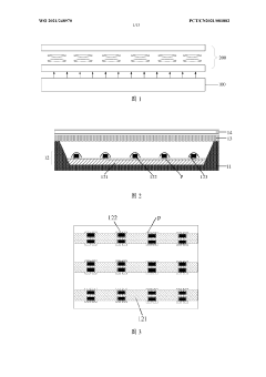
Display apparatus
PatentWO2021248970A1
Innovation
- Design a display device, in which at least two micro light-emitting diodes are soldered on at least one pad on the circuit board, and the reliability of the welding and the reflectivity of light are improved through the solder resist layer and the packaging layer to ensure the shunt driving and operation of the micro light-emitting diodes. Fault tolerance, reducing the probability of maintenance.
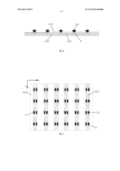
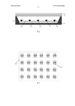
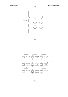
Display device
PatentWO2021104494A1
Innovation
- Design a display device that uses a reflective coating window structure. The thickness of the reflective coating is greater than or equal to the height of the Mini LED. The inner surface of the window is tilted to receive and reflect large-angle outgoing light, reducing the incidence of light into the protective layer and air interaction. The incident angle of the interface avoids total reflection and reduces material usage by dot-coating protective glue.


Standardization and Calibration Protocols for Mini LED Measurements
Standardized measurement protocols are essential for ensuring consistency and reliability in Mini LED resolution assessment across different devices and testing environments. The industry currently faces significant challenges due to the lack of universally accepted calibration standards specifically designed for Mini LED technology. Existing protocols often derive from traditional LED or LCD measurement methodologies, which fail to address the unique characteristics of Mini LED displays, particularly their high pixel density and localized dimming capabilities.
To establish effective standardization, measurement protocols must incorporate precise definitions of resolution metrics tailored to Mini LED technology. These metrics should include not only pixel count and density but also contrast ratio measurements under various ambient lighting conditions, color accuracy parameters, and response time specifications. The calibration process requires reference standards that account for the specific light emission patterns and potential crosstalk effects inherent to Mini LED arrays.
Temperature stabilization represents a critical factor in standardized measurements, as Mini LED performance characteristics can vary significantly with operating temperature. Protocols should mandate specific warm-up periods and environmental controls to ensure measurements occur under consistent thermal conditions. Additionally, standardized viewing angles and distances must be established to account for the directional nature of Mini LED light emission.
Calibration equipment requirements constitute another vital component of standardization efforts. High-resolution spectroradiometers with appropriate spatial resolution capabilities are necessary to accurately capture the performance of individual Mini LED zones. The industry needs to establish minimum specifications for measurement devices, including sensitivity thresholds, sampling rates, and optical filtering requirements specifically optimized for Mini LED characteristics.
Validation methodologies form the cornerstone of reliable measurement protocols. These should include procedures for verifying calibration accuracy through reference displays or certified test patterns. Round-robin testing among different laboratories can help identify and minimize systematic measurement variations. Furthermore, protocols should specify statistical methods for analyzing measurement uncertainty and establishing confidence intervals for reported resolution values.
Implementation of these standardized protocols requires industry-wide collaboration through organizations such as VESA, SID, and IEEE. The development of certification programs would enable manufacturers to demonstrate compliance with established measurement standards, ultimately benefiting consumers through more consistent and comparable product specifications. As Mini LED technology continues to evolve, these protocols must incorporate provisions for periodic review and updates to accommodate technological advancements and emerging display characteristics.
Integration with Production Line Automation Systems
The integration of real-time Mini LED resolution measurement systems with production line automation represents a critical advancement in manufacturing efficiency and quality control. Modern Mini LED production facilities require seamless connectivity between inspection equipment and broader manufacturing execution systems (MES) to maintain competitive production rates while ensuring consistent quality standards. This integration enables immediate feedback loops that can trigger automated adjustments to production parameters when resolution measurements fall outside acceptable thresholds.
Industry 4.0 protocols such as OPC UA (Open Platform Communications Unified Architecture) and MQTT (Message Queuing Telemetry Transport) have emerged as preferred communication standards for connecting resolution measurement systems with production line controllers. These protocols facilitate secure, reliable data exchange between measurement devices and central automation systems, allowing for real-time decision-making based on resolution metrics.
Implementation typically involves hardware interfaces such as industrial Ethernet connections or fieldbus systems that connect measurement equipment to programmable logic controllers (PLCs). These connections must support high-speed data transmission to accommodate the substantial data volumes generated by high-resolution optical measurement systems operating at production speeds exceeding 10,000 panels per hour.
Software integration layers play an equally important role, with middleware solutions translating measurement data into actionable commands for production equipment. Advanced implementations incorporate machine learning algorithms that analyze resolution measurement trends to predict potential defects before they occur, enabling preemptive maintenance or process adjustments.
Database integration ensures that resolution measurement data becomes part of the product's digital twin and manufacturing history. This historical data proves invaluable for traceability, process optimization, and compliance with industry standards such as JEDEC or customer-specific requirements. Cloud connectivity options further extend these capabilities by enabling remote monitoring and analysis of resolution measurement data across multiple production facilities.
Return on investment for such integration typically manifests through reduced scrap rates, with integrated systems showing 15-30% improvements in first-pass yield compared to manual inspection processes. Labor efficiency also improves significantly, with automated systems requiring approximately 60% less human intervention for quality control functions while maintaining higher consistency in measurement results.
Challenges in implementation include synchronization of measurement timing with production line takt time, ensuring measurement systems can operate at line speeds without becoming bottlenecks. Additionally, environmental factors such as vibration and electromagnetic interference must be mitigated to maintain measurement accuracy within the dynamic production environment.
Unlock deeper insights with Patsnap Eureka Quick Research — get a full tech report to explore trends and direct your research. Try now!
Generate Your Research Report Instantly with AI Agent
Supercharge your innovation with Patsnap Eureka AI Agent Platform!