Conductivity Scaling in Transparent Oxides for Consumer Electronics
SEP 19, 20259 MIN READ
Generate Your Research Report Instantly with AI Agent
Patsnap Eureka helps you evaluate technical feasibility & market potential.
Transparent Oxide Conductivity Evolution and Objectives
Transparent conductive oxides (TCOs) have evolved significantly over the past several decades, transforming from laboratory curiosities to essential components in modern consumer electronics. The journey began in the 1950s with the development of tin-doped indium oxide (ITO), which remains the industry standard despite ongoing challenges. The evolution of these materials has been driven by the dual requirements of high electrical conductivity and optical transparency, properties that are fundamentally in opposition according to classical electromagnetic theory.
The technological progression of TCOs has been marked by several key milestones. Early developments focused primarily on improving the conductivity of ITO through enhanced deposition techniques and doping strategies. The 2000s witnessed a paradigm shift with the emergence of alternative TCO materials such as aluminum-doped zinc oxide (AZO) and fluorine-doped tin oxide (FTO), addressing concerns about indium scarcity and cost. Most recently, the field has expanded to include novel materials like amorphous oxide semiconductors and carbon-based transparent conductors.
Current technological objectives in TCO development center around several critical parameters. Achieving sheet resistances below 10 ohms/square while maintaining optical transmittance above 90% in the visible spectrum represents the gold standard for next-generation displays and touch panels. Additionally, there is a growing emphasis on mechanical flexibility to support the burgeoning flexible electronics market, with targets for bending radii below 1mm without performance degradation.
Environmental and economic sustainability has emerged as another crucial objective in TCO development. The industry aims to reduce or eliminate dependence on scarce elements like indium, with research increasingly focused on earth-abundant alternatives. Process temperature reduction is also a key goal, with ambient temperature deposition techniques being developed to enable compatibility with temperature-sensitive substrates and reduce energy consumption.
Looking forward, the field is moving toward multifunctional TCOs that offer capabilities beyond simple conductivity and transparency. These include self-cleaning properties, antimicrobial functionality, and tunable work functions for improved device integration. The ultimate objective is to develop TCOs with conductivities approaching those of metals (>10^5 S/cm) while maintaining optical transparency above 95%, potentially revolutionizing applications from solar cells to advanced displays and smart windows.
The scaling of conductivity in transparent oxides represents one of the most significant challenges and opportunities in materials science today, with implications spanning virtually every segment of consumer electronics manufacturing and performance.
Market Analysis for Transparent Conductive Materials
The transparent conductive materials market has witnessed significant growth in recent years, primarily driven by the expanding consumer electronics sector. Currently valued at approximately $8.5 billion, this market is projected to reach $12.7 billion by 2027, representing a compound annual growth rate (CAGR) of 8.3%. This growth trajectory is largely attributed to the increasing demand for touchscreens, displays, and other interactive electronic devices that require materials combining optical transparency with electrical conductivity.
Indium Tin Oxide (ITO) continues to dominate the market with over 70% market share due to its established manufacturing processes and reliable performance characteristics. However, supply constraints and price volatility of indium have prompted manufacturers to explore alternative materials. Silver nanowires, carbon nanotubes, graphene, and metal mesh technologies are gaining traction, collectively accounting for about 25% of the market and expected to grow at a faster rate than traditional ITO.
Regional analysis reveals Asia-Pacific as the largest market for transparent conductive materials, contributing approximately 65% of global revenue. This dominance stems from the concentration of consumer electronics manufacturing in countries like China, South Korea, and Japan. North America and Europe follow with 18% and 12% market shares respectively, with particular growth in specialized applications such as automotive displays and photovoltaics.
By application segment, displays (including smartphones, tablets, and televisions) represent the largest market segment at 58%, followed by touchscreens at 22%. Emerging applications in photovoltaics, smart windows, and OLED lighting collectively account for 15% of the market but are experiencing the highest growth rates, exceeding 12% annually.
Consumer preferences are increasingly driving market dynamics, with demand for flexible, foldable, and wearable devices creating new requirements for transparent conductive materials. This shift has accelerated research into materials that maintain conductivity under bending and stretching conditions, with market research indicating that 35% of consumers express interest in flexible display technologies for their next device purchase.
Price sensitivity remains a critical factor, particularly in mass-market consumer electronics. Current production costs for ITO alternatives remain 30-40% higher than traditional ITO, presenting a significant barrier to widespread adoption. However, economies of scale and manufacturing innovations are gradually reducing this gap, with projections suggesting price parity for certain alternatives by 2025.
Current Limitations in Transparent Oxide Conductivity
Despite significant advancements in transparent oxide conductors, several fundamental limitations continue to impede their widespread adoption in consumer electronics applications. The primary challenge remains the inherent trade-off between optical transparency and electrical conductivity. As carrier concentration increases to improve conductivity, plasma frequency shifts toward the visible spectrum, reducing transparency. This fundamental physics constraint has proven difficult to overcome with conventional materials engineering approaches.
Material stability presents another significant barrier, particularly in flexible display applications where mechanical stress can induce microcracks that dramatically reduce conductivity over time. Current transparent oxides like ITO (Indium Tin Oxide) exhibit brittle characteristics with fracture strains typically below 2%, making them unsuitable for next-generation flexible consumer devices without substantial modification.
Processing limitations further restrict conductivity scaling. High-temperature annealing processes required to achieve optimal crystallinity and carrier mobility often exceed 300°C, making them incompatible with temperature-sensitive substrates used in modern electronics manufacturing. Lower temperature processes result in increased grain boundaries and defects that act as scattering centers, reducing overall conductivity by 30-50% compared to theoretical maximums.
Indium scarcity represents a critical supply chain constraint, with over 70% of global ITO production dependent on this relatively rare element. Price volatility and geopolitical factors affecting indium supply create significant risks for mass-market consumer electronics that require cost stability and reliable material sourcing.
Interface effects at the nanoscale further limit conductivity in thin films required for modern device architectures. Carrier depletion regions at material boundaries can extend 5-10nm into the conductive layer, significantly impacting overall performance in films below 50nm thickness. This becomes increasingly problematic as device miniaturization continues to demand thinner transparent conductive layers.
Current doping strategies have reached efficiency plateaus, with dopant solubility limits and increased ionized impurity scattering offsetting the benefits of higher carrier concentrations beyond certain thresholds. This creates diminishing returns in conductivity improvement despite increased material complexity and processing costs.
Environmental stability also remains problematic, with many high-performance transparent oxides showing degradation under humidity, UV exposure, and temperature cycling typical in consumer use scenarios. This necessitates additional protective layers that increase manufacturing complexity and potentially reduce optical performance.
Existing Conductivity Enhancement Methodologies
01 Transparent Conductive Oxide (TCO) Materials Composition
Various metal oxide compositions are used to create transparent conductive materials. These typically include indium tin oxide (ITO), zinc oxide (ZnO), and other doped metal oxides. The composition can be modified with dopants to enhance conductivity while maintaining optical transparency. These materials balance electrical conductivity with high visible light transmittance, making them suitable for optoelectronic applications.- Composition and structure of transparent conductive oxides: Transparent conductive oxides (TCOs) are materials that combine optical transparency with electrical conductivity. These materials typically consist of metal oxides such as indium tin oxide (ITO), zinc oxide (ZnO), or gallium-doped zinc oxide (GZO). The composition and crystal structure of these materials significantly influence their electrical and optical properties. Various dopants can be incorporated into the oxide matrix to enhance conductivity while maintaining transparency in the visible spectrum.
- Deposition methods for transparent conductive oxide films: Various deposition techniques are employed to fabricate transparent conductive oxide films with optimal properties. These methods include sputtering, chemical vapor deposition (CVD), atomic layer deposition (ALD), and sol-gel processes. The deposition parameters such as temperature, pressure, and gas flow rates significantly affect the film quality, crystallinity, and consequently the conductivity of the transparent oxide films. Post-deposition treatments like annealing can further enhance the electrical properties while maintaining optical transparency.
- Applications of transparent conductive oxides in electronic devices: Transparent conductive oxides are widely used in various electronic and optoelectronic devices. They serve as transparent electrodes in solar cells, light-emitting diodes (LEDs), flat panel displays, and touch screens. The combination of high electrical conductivity and optical transparency makes these materials ideal for applications where light needs to pass through while maintaining electrical functionality. Recent developments focus on improving the performance of these materials for flexible electronics and next-generation display technologies.
- Novel materials and doping strategies for enhanced conductivity: Research on new materials and doping strategies aims to enhance the conductivity of transparent oxides. This includes exploring alternative materials to traditional indium-based TCOs, such as aluminum-doped zinc oxide (AZO) and fluorine-doped tin oxide (FTO). Various doping elements and concentrations are investigated to optimize the carrier concentration and mobility in these materials. Composite structures and multilayer films are also developed to achieve a better balance between conductivity and transparency.
- Processing techniques for improving conductivity-transparency trade-off: Various processing techniques are employed to improve the trade-off between conductivity and transparency in oxide materials. These include controlled annealing processes, plasma treatments, and surface modifications. Nanostructuring approaches, such as creating patterned surfaces or incorporating nanoparticles, can enhance light transmission while maintaining good electrical pathways. Advanced manufacturing methods are also developed to produce TCO films with reduced defects and improved crystallinity, leading to better overall performance.
02 Deposition Methods for TCO Films
Different deposition techniques are employed to create transparent conductive oxide films with optimal properties. These methods include sputtering, chemical vapor deposition (CVD), sol-gel processes, and atomic layer deposition (ALD). The deposition parameters significantly affect the crystallinity, thickness uniformity, and ultimately the conductivity and transparency of the resulting films.Expand Specific Solutions03 TCO Applications in Solar Cells and Photovoltaics
Transparent conductive oxides are crucial components in solar cell technology, serving as electrodes that allow light to pass through while collecting generated current. The performance of photovoltaic devices depends on the TCO's sheet resistance, optical transmittance, and interface properties. Innovations in TCO materials have led to improved efficiency in thin-film solar cells and other photovoltaic applications.Expand Specific Solutions04 TCO Implementation in Display Technologies
Transparent conductive oxides are essential in display technologies such as LCDs, OLEDs, and touch screens. The conductivity and transparency properties of these materials directly impact display performance, including response time, power consumption, and visual clarity. Advanced TCO formulations enable the development of flexible, transparent displays and touch-sensitive interfaces.Expand Specific Solutions05 Post-Treatment Methods to Enhance TCO Properties
Various post-deposition treatments can significantly improve the conductivity of transparent oxide films. These include thermal annealing, plasma treatment, laser processing, and chemical treatments. Such processes can modify the crystal structure, reduce defects, and optimize carrier concentration, resulting in enhanced electrical conductivity while maintaining optical transparency.Expand Specific Solutions
Leading Manufacturers and Research Institutions
The transparent oxide conductivity scaling market for consumer electronics is in a growth phase, with increasing demand driven by the proliferation of touch screens, displays, and flexible electronics. The market size is expanding rapidly, projected to reach significant value as applications diversify beyond traditional displays into emerging sectors like wearables and IoT devices. Technologically, the field shows varying maturity levels across players: established companies like Samsung Electronics, Sharp, and Micron Technology demonstrate advanced commercial implementation, while research-focused entities like IMEC, Oregon State University, and Semiconductor Energy Laboratory are pushing boundaries with novel materials and fabrication techniques. Companies like TDK, JSR Corp, and Idemitsu Kosan are leveraging their materials expertise to develop next-generation transparent conductive oxides with enhanced performance-to-cost ratios, positioning themselves for future market expansion.
Semiconductor Energy Laboratory Co., Ltd.
Technical Solution: Semiconductor Energy Laboratory (SEL) has developed crystalline oxide semiconductor technology that addresses conductivity scaling challenges through atomic-level control of material composition. Their c-axis aligned crystalline indium-gallium-zinc oxide (CAAC-IGZO) technology represents a breakthrough in transparent oxide conductivity, achieving electron mobility exceeding 40 cm²/Vs while maintaining transparency above 85%. SEL's approach focuses on controlling oxygen vacancy concentration and distribution through precise annealing processes and composition modulation. Their patented deposition techniques create highly ordered crystalline structures that minimize grain boundary scattering, a common limitation in conventional TCOs. SEL has also pioneered the integration of these materials into ultra-low power display backplanes, demonstrating power consumption reductions of up to 80% compared to amorphous silicon technologies. Their manufacturing process is compatible with large-area substrates, enabling scalable production for consumer electronics applications.
Strengths: Superior electron mobility compared to amorphous oxide semiconductors; excellent stability under environmental stresses; compatibility with existing manufacturing infrastructure. Weaknesses: Higher processing temperatures than amorphous alternatives; more complex manufacturing process requiring precise control; challenges with uniformity across large substrates.
Interuniversitair Micro-Electronica Centrum VZW
Technical Solution: IMEC has developed cutting-edge transparent conductive oxide technologies focusing on atomic layer deposition (ALD) of zinc tin oxide (ZTO) and hydrogen-doped indium oxide (In2O3:H) for next-generation consumer electronics. Their approach achieves conductivity scaling through precise control of material composition and nanostructure. IMEC's hydrogen-doped indium oxide has demonstrated mobility exceeding 100 cm²/Vs while maintaining transparency above 90% in the visible spectrum. Their patented two-step deposition process combines room-temperature ALD with controlled post-deposition annealing, enabling precise tuning of carrier concentration without compromising transparency. IMEC has also pioneered area-selective deposition techniques that eliminate the need for etching steps, reducing manufacturing complexity and improving interface quality. Their recent work has focused on developing indium-free alternatives based on molybdenum-doped zinc oxide that achieve sheet resistance below 20 ohms/square while eliminating dependence on scarce elements.
Strengths: Advanced atomic-level deposition control enabling precise material engineering; strong intellectual property portfolio; excellent integration capabilities with semiconductor manufacturing processes. Weaknesses: Limited large-scale manufacturing experience compared to industrial players; higher initial implementation costs; challenges with technology transfer to production environments.
Breakthrough Patents in Transparent Oxide Scaling
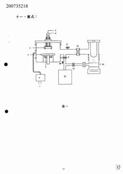
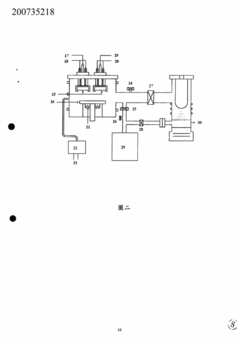
A method for indium oxide and its related materials to improve their conductivity and transparency
PatentInactiveTW200735218A
Innovation
- Incorporating carbon into the manufacturing process of indium oxide-based materials, either before or after annealing, through methods like ion implantation, gas diffusion, or sputtering, to enhance conductivity and light transmittance.
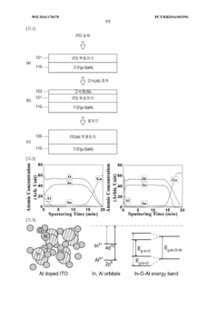
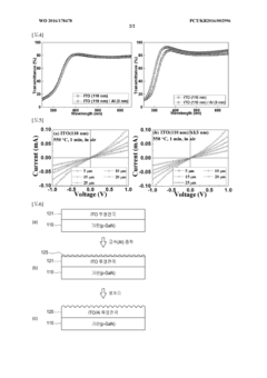
Method of forming transparent electrode having improved transmissivity, and semiconductor device including transparent electrode formed by using same
PatentWO2016178478A1
Innovation
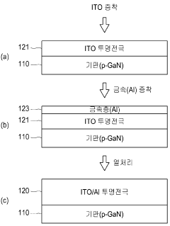
- A method involving the deposition of indium oxide and tin oxide to form an ITO transparent electrode, followed by the formation of a metal layer with elements like Al, Ti, or Ge, which are lower in the periodic table than indium, and subsequent heat treatment to penetrate these metals into the ITO electrode, expanding the effective band gap and improving conductivity.
Supply Chain Considerations for TCO Materials
The global supply chain for Transparent Conductive Oxide (TCO) materials represents a complex ecosystem that significantly impacts the advancement of conductivity scaling in consumer electronics. Raw material sourcing for TCOs, particularly indium for ITO (Indium Tin Oxide), faces substantial challenges due to geographical concentration in China, South Korea, and Japan, which control approximately 70% of global indium production. This concentration creates vulnerability to geopolitical tensions and trade restrictions, potentially disrupting the consistent supply needed for high-volume consumer electronics manufacturing.
Material processing capabilities present another critical consideration, as the production of high-quality TCO films requires specialized equipment and expertise. The manufacturing infrastructure is predominantly established in East Asia, with significant capacity gaps in North America and Europe. This regional imbalance necessitates complex logistics networks and increases dependency on specific manufacturing hubs, potentially limiting rapid scaling of new TCO technologies.
Cost volatility represents a significant barrier to widespread implementation of advanced TCO solutions. Indium prices have fluctuated by over 300% in the past decade, compelling manufacturers to develop alternative materials like aluminum-doped zinc oxide (AZO) and fluorine-doped tin oxide (FTO). These alternatives, while promising, often require substantial modifications to existing production lines, creating additional supply chain complexities during transition periods.
Environmental regulations increasingly influence TCO material supply chains, with restrictions on certain processing chemicals and growing requirements for sustainable sourcing. The European Union's REACH regulations and similar frameworks in other regions impose compliance costs that must be factored into supply chain planning. Manufacturers pursuing advanced conductivity in transparent oxides must navigate these regulatory landscapes while maintaining cost competitiveness.
Vertical integration strategies have emerged as a response to supply chain vulnerabilities, with major consumer electronics companies securing direct access to raw materials and processing capabilities. Companies like Samsung and LG have invested in partnerships with mining operations and material refiners to ensure consistent access to critical TCO components, providing competitive advantages in scaling conductivity improvements to mass production.
Recycling infrastructure for TCO materials remains underdeveloped despite its potential to mitigate supply risks. Current recovery rates for indium from end-of-life electronics hover below 1%, representing a significant missed opportunity for circular economy approaches that could stabilize material availability for next-generation transparent conductive applications in consumer electronics.
Environmental Impact of Transparent Oxide Production
The production of transparent conductive oxides (TCOs) for consumer electronics presents significant environmental challenges that warrant careful consideration in the scaling of this technology. Raw material extraction for TCOs, particularly indium for indium tin oxide (ITO), involves energy-intensive mining operations that contribute to habitat destruction, soil erosion, and water pollution. The scarcity of indium as a critical material further exacerbates these environmental concerns, with estimates suggesting that economically viable reserves may be depleted within decades at current consumption rates.
Manufacturing processes for transparent oxides typically require high-temperature deposition techniques such as sputtering, chemical vapor deposition, or sol-gel methods, all of which demand substantial energy inputs. The carbon footprint associated with these energy requirements is considerable, with some studies indicating that the production of TCO layers for a single large-format display panel can generate CO2 emissions equivalent to driving a passenger vehicle for several hundred kilometers.
Chemical waste management presents another significant environmental challenge in TCO production. Etching processes utilize hazardous acids and solvents that require specialized disposal protocols. Improper handling of these chemicals can lead to groundwater contamination and adverse health effects for workers and surrounding communities. Additionally, the precursor materials used in certain deposition methods contain toxic compounds that necessitate stringent safety measures during manufacturing.
Recycling and end-of-life considerations for transparent oxide components remain underdeveloped compared to other electronic materials. The complex integration of TCOs with other materials in consumer devices makes separation and recovery technically challenging and economically prohibitive. Current estimates suggest that less than 1% of indium from discarded electronics is successfully recovered, representing a substantial loss of a valuable resource and contributing to electronic waste accumulation.
Alternative TCO materials with reduced environmental impact are emerging as potential solutions. Aluminum-doped zinc oxide (AZO) and fluorine-doped tin oxide (FTO) utilize more abundant elements, potentially reducing the ecological footprint associated with raw material extraction. Additionally, research into low-temperature deposition methods shows promise for decreasing energy consumption during manufacturing, with some novel techniques achieving comparable film quality at temperatures below 200°C.
Regulatory frameworks addressing the environmental impact of TCO production vary significantly across regions, creating challenges for global supply chains. The European Union's Restriction of Hazardous Substances (RoHS) and Registration, Evaluation, Authorization and Restriction of Chemicals (REACH) regulations have driven improvements in manufacturing practices, but implementation remains inconsistent in other manufacturing hubs.
Unlock deeper insights with Patsnap Eureka Quick Research — get a full tech report to explore trends and direct your research. Try now!
Generate Your Research Report Instantly with AI Agent
Supercharge your innovation with Patsnap Eureka AI Agent Platform!