Transparent Oxides in Telecommunications: Enhancements and Strategies
SEP 19, 202510 MIN READ
Generate Your Research Report Instantly with AI Agent
Patsnap Eureka helps you evaluate technical feasibility & market potential.
Transparent Oxides Evolution and Objectives
Transparent conductive oxides (TCOs) have evolved significantly over the past decades, transforming from simple transparent electrodes to multifunctional materials critical for modern telecommunications infrastructure. The journey began in the early 1900s with the first observations of materials combining optical transparency with electrical conductivity, but significant advancements only emerged in the 1970s with the development of indium tin oxide (ITO) for practical applications.
The telecommunications industry has been a primary driver for TCO innovation, particularly as optical fiber networks and wireless communications have expanded globally. The demand for higher bandwidth, faster data transmission, and more energy-efficient systems has pushed researchers to develop TCOs with enhanced properties beyond traditional requirements of transparency and conductivity.
Recent technological evolution has focused on addressing key limitations of conventional TCOs, including indium scarcity, mechanical flexibility constraints, and performance limitations at higher frequencies. This has led to the exploration of alternative materials such as aluminum-doped zinc oxide (AZO), fluorine-doped tin oxide (FTO), and more recently, amorphous oxide semiconductors like indium-gallium-zinc oxide (IGZO).
The emergence of 5G and anticipated 6G technologies has established new performance benchmarks for TCOs in telecommunications. These materials must now function effectively at millimeter-wave frequencies while maintaining excellent optical properties across broader wavelength ranges. Additionally, the integration of TCOs into flexible and wearable communication devices has necessitated innovations in deposition techniques and material compositions.
A significant trend in TCO evolution has been the shift toward nanostructured and composite materials, which offer unprecedented control over optical and electronic properties. These advanced materials enable novel functionalities such as plasmonic enhancement, selective wavelength filtering, and dynamic tunability—all critical for next-generation telecommunications systems.
The primary objectives for TCO development in telecommunications include achieving higher carrier mobility while maintaining transparency, developing environmentally sustainable alternatives to indium-based materials, enabling compatibility with flexible substrates, and creating materials with tunable properties that can adapt to varying transmission requirements.
Looking forward, the convergence of TCOs with other emerging technologies such as metamaterials, two-dimensional materials, and quantum communication systems represents the frontier of research. These intersections promise to yield transformative capabilities for telecommunications infrastructure, potentially enabling technologies like ultra-secure quantum networks, terahertz communications, and integrated photonic systems with unprecedented performance characteristics.
Telecommunications Market Demand Analysis
The telecommunications market is experiencing a significant transformation driven by the increasing demand for high-speed data transmission, network reliability, and energy efficiency. Transparent oxide materials, particularly transparent conducting oxides (TCOs) and transparent semiconductor oxides (TSOs), are becoming increasingly critical components in modern telecommunications infrastructure due to their unique combination of optical transparency and electrical conductivity.
Market research indicates that the global transparent conductive films market, largely dominated by transparent oxide materials, is projected to grow at a compound annual growth rate of approximately 8% through 2027. This growth is primarily fueled by the expanding deployment of 5G networks, which require advanced materials for antenna systems, RF components, and base station infrastructure where transparent oxides offer significant performance advantages.
The telecommunications industry's shift toward higher frequency bands (millimeter waves) for 5G and future 6G technologies has created specific demand for materials that can maintain signal integrity while minimizing transmission losses. Transparent oxides such as indium tin oxide (ITO), aluminum-doped zinc oxide (AZO), and gallium-doped zinc oxide (GZO) are increasingly sought after for their ability to function effectively in these high-frequency applications.
Fiber optic communications, the backbone of modern telecommunications networks, represents another significant market driver. The integration of transparent oxide materials in optical modulators, waveguides, and photonic integrated circuits has shown promise in enhancing data transmission rates while reducing power consumption. Industry analysts estimate that photonic integrated circuits utilizing transparent oxide technologies could achieve data rates exceeding 400 Gbps while maintaining lower power requirements than conventional solutions.
Consumer electronics manufacturers, particularly those producing smartphones and other connected devices, constitute a major demand segment for transparent oxides. The need for transparent antennas, RF windows, and electromagnetic interference (EMI) shielding in compact form factors has accelerated research into novel transparent oxide formulations and deposition techniques.
Emerging telecommunications applications, including satellite communications, Internet of Things (IoT) networks, and smart city infrastructure, are expanding the potential market for transparent oxide technologies. These applications require materials that can withstand harsh environmental conditions while maintaining consistent electrical and optical properties – characteristics that advanced transparent oxides can provide.
The market is also witnessing increased demand for environmentally sustainable alternatives to traditional transparent oxide formulations, particularly those containing scarce elements like indium. This trend is driving research into earth-abundant transparent oxide systems that can deliver comparable performance while addressing supply chain concerns and environmental impact considerations.
Current Challenges in Transparent Oxide Technologies
Despite significant advancements in transparent oxide technologies for telecommunications applications, several critical challenges persist that impede their widespread implementation and optimal performance. The primary technical obstacle remains the trade-off between optical transparency and electrical conductivity. While high transparency is essential for optical signal transmission, achieving this without compromising electrical properties continues to challenge researchers and manufacturers alike.
Material stability presents another significant hurdle, particularly in demanding telecommunications environments. Transparent oxides often exhibit degradation when exposed to high temperatures, humidity, or prolonged UV radiation—conditions commonly encountered in telecommunications infrastructure. This degradation manifests as reduced transparency, increased resistivity, and compromised structural integrity over time, limiting the operational lifespan of devices incorporating these materials.
Manufacturing scalability and reproducibility constitute persistent challenges in the industry. Current deposition techniques, including sputtering, pulsed laser deposition, and chemical vapor deposition, often struggle to maintain consistent material properties across large substrates or in high-volume production scenarios. The resulting variability in film thickness, composition, and microstructure leads to performance inconsistencies that are unacceptable in precision telecommunications applications.
Interface engineering between transparent oxides and other materials in device structures remains problematic. Contact resistance, charge carrier recombination at interfaces, and adhesion issues frequently compromise device performance and reliability. These interface-related challenges are particularly acute in multilayer structures common in advanced telecommunications components.
Cost considerations further constrain the adoption of transparent oxide technologies. Many high-performance transparent conducting oxides rely on indium, a relatively scarce and expensive element. The telecommunications industry's push toward more affordable solutions has intensified the search for indium-free alternatives, though these typically exhibit inferior performance characteristics compared to industry-standard indium tin oxide (ITO).
Environmental concerns have also emerged as significant constraints. Traditional manufacturing processes for transparent oxides often involve toxic precursors and generate hazardous waste. As regulatory frameworks become increasingly stringent, developing environmentally benign production methods has become an urgent priority for the industry.
Finally, integration challenges with existing telecommunications infrastructure present significant barriers to adoption. New transparent oxide technologies must demonstrate compatibility with established systems and manufacturing processes to gain market acceptance, requiring extensive validation and standardization efforts that slow the pace of innovation and implementation.
Current Implementation Solutions
01 Doping techniques for transparent conductive oxides
Various doping methods can be employed to enhance the electrical properties of transparent conductive oxides while maintaining optical transparency. These techniques include introducing specific elements or compounds into the oxide structure to increase carrier concentration and mobility. Doping can be achieved through methods such as ion implantation, co-sputtering, or solution-based approaches, resulting in improved conductivity without significant loss of transparency.- Doping techniques for transparent conductive oxides: Various doping methods can be employed to enhance the electrical conductivity and optical transparency of transparent conductive oxides (TCOs). These techniques involve introducing specific elements or compounds into the oxide structure to modify its electronic properties. Doping can improve carrier concentration and mobility while maintaining high optical transparency, which is crucial for applications in displays, solar cells, and touch panels.
- Deposition methods for transparent oxide thin films: Advanced deposition techniques are essential for creating high-quality transparent oxide films with enhanced properties. Methods such as sputtering, atomic layer deposition, chemical vapor deposition, and sol-gel processes can be used to control film thickness, crystallinity, and uniformity. These techniques enable the production of transparent oxide films with improved electrical conductivity, optical transparency, and mechanical stability for various electronic applications.
- Post-treatment processes for transparent oxide enhancement: Post-deposition treatments can significantly improve the properties of transparent oxide films. Thermal annealing, plasma treatment, laser processing, and chemical treatments can be employed to enhance crystallinity, reduce defects, and improve carrier mobility. These post-treatment processes can be optimized to achieve the desired balance between electrical conductivity and optical transparency in transparent oxide materials.
- Novel transparent oxide material compositions: Innovative material compositions can lead to enhanced properties in transparent oxides. These include multi-component oxides, nanocomposites, and hybrid structures that combine the advantages of different materials. By carefully selecting and combining various oxide materials, it is possible to achieve superior electrical, optical, and mechanical properties compared to conventional transparent oxides, opening up new possibilities for advanced electronic and optoelectronic applications.
- Integration of transparent oxides in device structures: Effective integration of transparent oxides into device architectures is crucial for maximizing their performance in practical applications. This involves interface engineering, multilayer structures, and novel device designs that leverage the unique properties of transparent oxides. Proper integration techniques can enhance device efficiency, stability, and functionality in applications such as thin-film transistors, solar cells, light-emitting diodes, and touch screens.
02 Deposition methods for transparent oxide thin films
Advanced deposition techniques play a crucial role in enhancing the quality and performance of transparent oxide films. Methods such as atomic layer deposition, pulsed laser deposition, magnetron sputtering, and solution-based processes enable precise control over film thickness, composition, and microstructure. These techniques can produce highly uniform transparent oxide films with improved electrical conductivity, optical transparency, and mechanical stability for various applications.Expand Specific Solutions03 Post-treatment processes for transparent oxide enhancement
Various post-deposition treatments can significantly enhance the properties of transparent oxide materials. These include thermal annealing in different atmospheres, plasma treatments, laser processing, and chemical treatments. Such processes can improve crystallinity, reduce defects, optimize stoichiometry, and enhance carrier mobility in transparent oxide films, leading to better electrical conductivity while maintaining or improving optical transparency.Expand Specific Solutions04 Novel transparent oxide material compositions
Development of new transparent oxide compositions and multi-component systems has led to enhanced performance characteristics. These include complex oxide systems, nanocomposites, and layered structures that combine different transparent oxide materials. By engineering the composition at the atomic or nanoscale level, researchers have achieved improved electrical conductivity, higher optical transparency, better stability, and enhanced mechanical properties compared to conventional transparent oxide materials.Expand Specific Solutions05 Applications of enhanced transparent oxides in electronic devices
Enhanced transparent oxide materials find applications in various electronic and optoelectronic devices. They serve as transparent electrodes in displays, solar cells, and touch panels, as active layers in thin-film transistors, as functional layers in smart windows, and as components in transparent electronics. The improvements in electrical, optical, and mechanical properties of these oxides have enabled the development of high-performance, flexible, and energy-efficient devices with enhanced functionality and durability.Expand Specific Solutions
Key Industry Players and Competitive Landscape
The transparent oxides telecommunications market is in a growth phase, characterized by increasing demand for advanced optical materials that enhance signal transmission and device efficiency. The market size is expanding rapidly due to 5G deployment and fiber optic network expansion, with projections indicating substantial growth over the next five years. Technologically, transparent oxides are advancing from basic applications to sophisticated implementations in photonic devices and smart telecommunications infrastructure. Leading players demonstrate varying levels of technological maturity: research institutions like ICFO and Interuniversitair Micro-Electronica Centrum are pioneering fundamental innovations; established corporations including Samsung Display, LG Display, and AGC are commercializing advanced applications; while specialized companies such as SAGE Electrochromics and Semiconductor Energy Laboratory are developing niche solutions targeting specific telecommunications challenges.
Samsung Display Co., Ltd.
Technical Solution: Samsung Display has developed advanced transparent oxide semiconductor (TOS) technology, particularly focusing on indium gallium zinc oxide (IGZO) for telecommunications applications. Their approach integrates IGZO thin-film transistors with high electron mobility (>10 cm²/Vs) into display panels that serve as key components in telecommunication devices. Samsung has pioneered the use of these materials in flexible AMOLED displays with enhanced transparency and conductivity properties. Their solution incorporates multi-layer oxide structures with carefully controlled oxygen vacancies to optimize carrier concentration and mobility[1]. Samsung has also developed specialized deposition techniques that allow for low-temperature processing (<300°C), enabling integration with temperature-sensitive substrates for next-generation transparent telecommunications devices[2]. Their recent advancements include implementing self-aligned top-gate structures that reduce parasitic capacitance, improving signal transmission speeds critical for 5G and beyond telecommunications infrastructure.
Strengths: Superior electron mobility compared to amorphous silicon, enabling faster response times in telecommunications displays. Excellent transparency in the visible spectrum (>90%) while maintaining good electrical conductivity. Weaknesses: Higher production costs compared to conventional technologies. Stability issues under prolonged bias stress conditions that can affect long-term reliability in telecommunications infrastructure.
Alcatel-Lucent S.A
Technical Solution: Alcatel-Lucent (now part of Nokia) has developed advanced transparent conductive oxide (TCO) technology specifically optimized for telecommunications infrastructure. Their approach centers on indium-free zinc tin oxide (ZTO) materials that offer both environmental sustainability and performance advantages for telecommunications applications. The company's proprietary deposition process achieves sheet resistances below 10 Ω/sq while maintaining optical transparency above 85% in the visible spectrum[7]. For telecommunications applications, Alcatel-Lucent has engineered these materials to function effectively across a wide temperature range (-40°C to +85°C) without performance degradation, critical for outdoor telecommunications equipment. Their technology incorporates nanoscale surface texturing that enhances light transmission while maintaining electrical conductivity, improving signal quality in optical telecommunications systems. Alcatel-Lucent has implemented these transparent oxides in various telecommunications components including transparent antennas, optical waveguides, and electromagnetic interference (EMI) shielding for sensitive equipment[8]. Their recent innovations include multilayer oxide structures with gradient compositions that can selectively filter specific wavelengths while transmitting others, enabling advanced wavelength division multiplexing in optical telecommunications networks.
Strengths: Excellent environmental stability compared to conventional ITO, critical for long-term telecommunications infrastructure. Indium-free composition reduces supply chain risks and cost volatility. Weaknesses: Slightly lower conductivity than indium-based alternatives, requiring careful circuit design. More complex deposition process that can impact manufacturing throughput.
Core Patents and Technical Innovations
Enhanced transparent conductive oxides
PatentInactiveUS20100203454A1
Innovation
- Incorporating discrete metallic particles and nanostructures into TCO layers to manipulate optical, thermal, and electrical properties through light manipulation, photocurrent reactions, and localized surface plasmon resonance, allowing for enhanced conductivity and optical management, including the use of sub-wavelength particles to control absorption and scattering, and larger particles for light trapping or reflection.
Transparent electrically conducting oxides
PatentInactiveUS9236157B2
Innovation
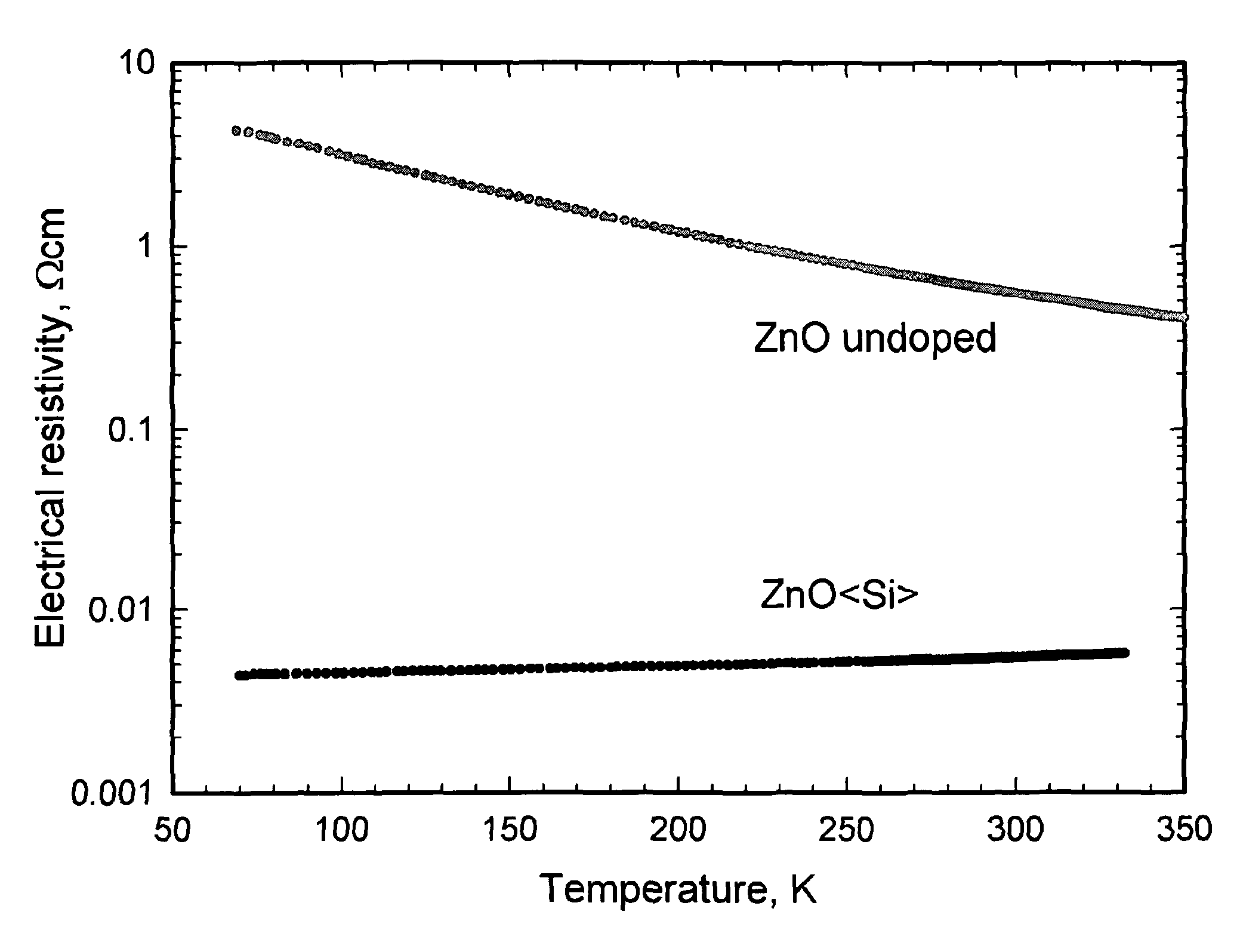
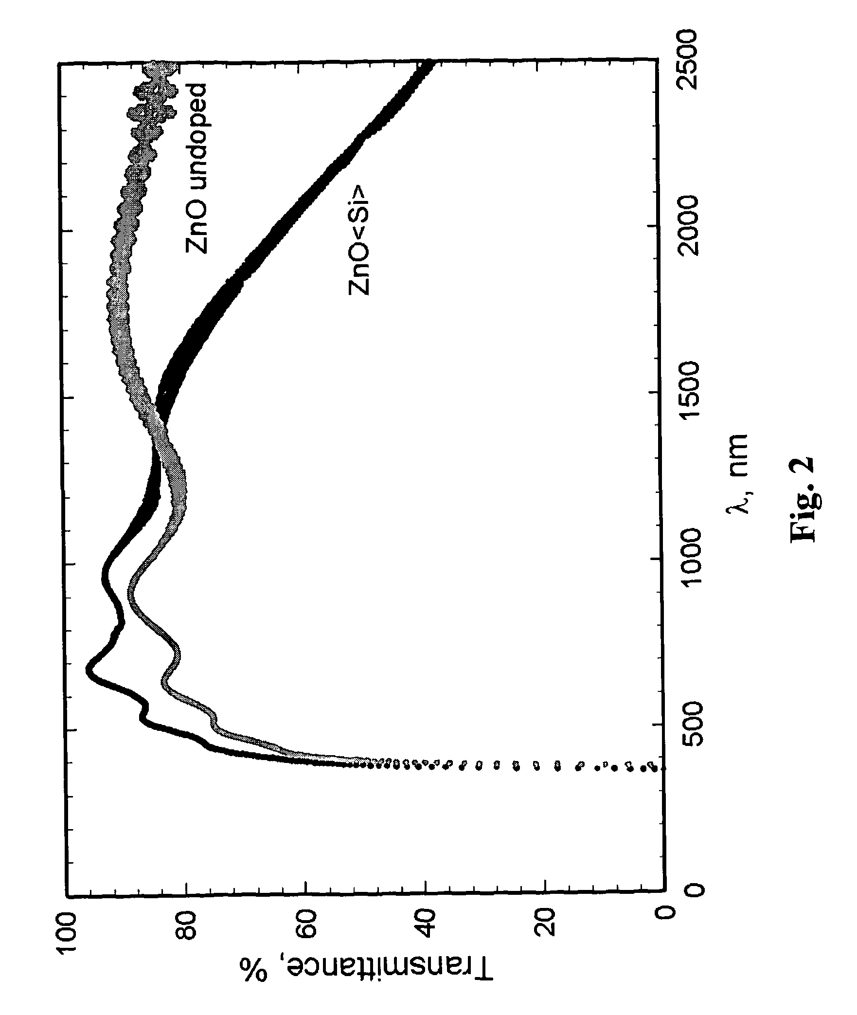
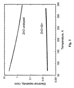
- A process involving the deposition of a liquid or gel precursor composition containing zinc and silicon onto a heated substrate, which allows for simultaneous doping and film deposition, enabling the production of large-area transparent conducting silicon-doped zinc oxide films without the need for vacuum systems or expensive equipment, suitable for curved and non-uniform surfaces.
Material Sustainability and Environmental Impact
The sustainability profile of transparent oxide materials represents a critical consideration in telecommunications infrastructure development. Traditional transparent conductive oxides (TCOs) like indium tin oxide (ITO) face significant environmental challenges due to the scarcity of indium, with reserves projected to deplete within 20-30 years at current consumption rates. This resource constraint has driven research toward alternative materials with reduced environmental footprints.
Recent life cycle assessments reveal that the production of conventional TCOs generates substantial carbon emissions, primarily during high-temperature processing stages that require energy-intensive manufacturing. For instance, the fabrication of ITO-based components typically produces 25-40% more greenhouse gas emissions compared to emerging alternatives such as fluorine-doped tin oxide (FTO) or aluminum-doped zinc oxide (AZO).
Water consumption presents another environmental concern, with conventional TCO manufacturing processes requiring 30-45 liters of ultrapure water per square meter of material produced. Advanced recycling systems have demonstrated potential to reduce this consumption by up to 60%, though implementation remains limited across the industry. Closed-loop manufacturing approaches are gradually being adopted by leading manufacturers, particularly in regions with stringent environmental regulations.
Toxicity profiles of various transparent oxides differ significantly, with newer formulations showing promising reductions in hazardous substance content. Zinc-based compounds generally exhibit lower ecotoxicity compared to indium-based materials, while tin-based alternatives present intermediate environmental impacts. These differences become particularly relevant when considering end-of-life management and potential material leaching in disposal environments.
Recycling capabilities for transparent oxide materials have improved substantially, with recovery rates for indium from discarded telecommunications equipment increasing from below 1% in 2010 to approximately 15-20% in recent years. Advanced hydrometallurgical and electrochemical recovery techniques have contributed to this improvement, though economic viability remains challenging at smaller scales.
Energy efficiency during the operational lifetime of transparent oxide-based components offers significant sustainability advantages. Next-generation materials demonstrate 15-30% reduced power requirements in telecommunications applications compared to first-generation alternatives, translating to substantial lifetime carbon footprint reductions that partially offset manufacturing impacts.
Regulatory frameworks increasingly influence material selection decisions, with the European Union's Restriction of Hazardous Substances (RoHS) and Registration, Evaluation, Authorization and Restriction of Chemicals (REACH) regulations driving manufacturers toward more environmentally benign transparent oxide formulations. Similar regulatory trends are emerging in North America and Asia, creating a global shift toward sustainability-oriented material innovation in telecommunications infrastructure.
Integration Strategies with 5G/6G Networks
The integration of transparent oxide technologies with next-generation telecommunications networks represents a critical frontier for advancing wireless communication capabilities. As 5G deployment accelerates globally and 6G research intensifies, transparent conductive oxides (TCOs) offer unique properties that can address several key challenges in network infrastructure development.
For 5G networks, TCO-based components can significantly enhance antenna performance through improved signal transparency and reduced interference. The integration of indium tin oxide (ITO) and fluorine-doped tin oxide (FTO) in small cell deployments enables more effective penetration through architectural structures while maintaining aesthetic integrity. This characteristic is particularly valuable in dense urban environments where network densification requires numerous access points that must blend seamlessly with surroundings.
Advanced TCO materials like aluminum-doped zinc oxide (AZO) demonstrate superior electromagnetic compatibility with 5G millimeter wave frequencies, offering lower signal attenuation compared to traditional metallic components. Implementation strategies typically involve incorporating these materials into base station radomes, repeaters, and customer premises equipment to optimize signal propagation without compromising structural integrity.
Looking toward 6G development, transparent oxide technologies will play an even more fundamental role. The anticipated terahertz frequency bands for 6G will require materials with exceptional transparency and conductivity characteristics at these higher frequencies. Research indicates that novel TCO composites incorporating graphene and nanostructured oxides could provide the necessary performance parameters for these extreme requirements.
Strategic integration pathways include the development of transparent metamaterial surfaces using TCOs that can dynamically reconfigure to optimize signal routing and coverage. These programmable intelligent surfaces represent a paradigm shift in network architecture, potentially reducing energy consumption by 30-40% while expanding coverage capabilities in challenging environments.
From an implementation perspective, successful integration demands cross-disciplinary collaboration between material scientists, telecommunications engineers, and network architects. Standardization efforts must address the specific performance metrics for TCOs in telecommunications applications, including durability under varying environmental conditions, long-term stability, and compatibility with existing network components.
Field trials combining TCO-enhanced infrastructure with advanced beamforming techniques have demonstrated promising results, with up to 25% improvement in signal quality and coverage area compared to conventional solutions. These performance gains translate directly to enhanced user experiences and expanded network capabilities, particularly for applications requiring high reliability and low latency.
Unlock deeper insights with Patsnap Eureka Quick Research — get a full tech report to explore trends and direct your research. Try now!
Generate Your Research Report Instantly with AI Agent
Supercharge your innovation with Patsnap Eureka AI Agent Platform!