

Transparent Oxides' Role in Non-Contact Sensor Development
SEP 19, 20259 MIN READ
Generate Your Research Report Instantly with AI Agent
PatSnap Eureka helps you evaluate technical feasibility & market potential.
Transparent Oxides Evolution and Sensing Objectives
Transparent oxides have emerged as a pivotal material class in the evolution of non-contact sensing technologies, marking significant milestones since their initial discovery in the early 20th century. The journey began with basic metal oxides like zinc oxide and tin oxide, which demonstrated unique electrical properties when exposed to environmental changes. By the 1960s, researchers recognized the potential of these materials for gas sensing applications, leading to the first generation of semiconductor-based gas sensors utilizing transparent oxide films.
The technological landscape transformed dramatically in the 1990s with the development of transparent conducting oxides (TCOs), particularly indium tin oxide (ITO), which combined optical transparency with electrical conductivity. This dual functionality opened new avenues for non-contact sensing applications where visual observation and electronic detection could occur simultaneously, a critical requirement for modern touchless interfaces and environmental monitoring systems.
Recent advancements have focused on amorphous oxide semiconductors (AOS), such as indium gallium zinc oxide (IGZO), which offer superior electron mobility and stability compared to their crystalline counterparts. These materials have enabled the development of thin-film transistors that can be integrated into flexible substrates, creating opportunities for wearable and conformable sensing devices that maintain performance integrity even under mechanical stress.
The primary objective in transparent oxide sensor development is achieving enhanced sensitivity while maintaining selectivity—a persistent challenge in the field. Current research aims to optimize material composition and nanostructuring to detect specific target analytes at increasingly lower concentrations, particularly important for environmental pollutants and biomarkers that present health risks even at trace levels.
Another critical goal is the development of self-powered sensing systems utilizing transparent oxides with photovoltaic properties. These materials can harvest ambient light to power sensor operations, eliminating the need for external power sources and enabling truly autonomous sensing networks for Internet of Things (IoT) applications.
Durability represents another significant objective, as sensors deployed in real-world environments must withstand temperature fluctuations, humidity variations, and exposure to potentially corrosive substances. Researchers are exploring composite structures and surface treatments to enhance the chemical stability and mechanical resilience of transparent oxide sensors without compromising their sensing capabilities.
Looking forward, the integration of transparent oxides with artificial intelligence presents perhaps the most transformative objective. Machine learning algorithms can be trained to recognize patterns in sensor data, enabling predictive capabilities and adaptive responses to environmental changes, ultimately creating intelligent sensing systems that can anticipate needs rather than simply react to conditions.
Market Analysis for Non-Contact Sensing Technologies
The non-contact sensing technologies market has experienced substantial growth in recent years, driven by increasing demand across multiple industries including healthcare, automotive, consumer electronics, and industrial automation. The global market for non-contact sensors was valued at approximately $10.2 billion in 2022 and is projected to reach $18.7 billion by 2028, representing a compound annual growth rate (CAGR) of 10.6% during the forecast period.
Transparent oxide-based sensors are emerging as a significant segment within this market, particularly in applications requiring both optical transparency and electrical functionality. These materials, including indium tin oxide (ITO), aluminum-doped zinc oxide (AZO), and gallium-doped zinc oxide (GZO), offer unique properties that enable development of innovative sensing solutions.
Healthcare applications represent the fastest-growing segment for transparent oxide-based non-contact sensors, with a projected CAGR of 12.8% through 2028. This growth is primarily driven by increasing adoption in medical imaging, patient monitoring systems, and touchless healthcare interfaces. The COVID-19 pandemic has accelerated this trend, creating heightened demand for contactless vital sign monitoring and diagnostic tools.
The automotive sector constitutes another major market for these technologies, valued at $2.3 billion in 2022. Advanced driver assistance systems (ADAS), gesture recognition interfaces, and occupancy detection systems are key application areas where transparent oxide sensors provide advantages over traditional technologies. Industry analysts predict that by 2026, over 70% of new vehicles will incorporate some form of transparent oxide-based sensing technology.
Consumer electronics applications, including smartphones, tablets, and wearable devices, account for approximately 35% of the current market share. The demand for edge-to-edge displays, in-display fingerprint sensors, and advanced touch interfaces is driving adoption of transparent oxide materials in this sector.
Regionally, Asia-Pacific dominates the market with a 42% share, followed by North America (28%) and Europe (22%). China and South Korea are leading in manufacturing capacity for transparent oxide materials, while North American and European companies focus on high-value applications and system integration.
Key market challenges include material cost fluctuations, particularly for indium-based compounds, and competition from alternative technologies such as PEDOT:PSS and silver nanowire networks. Environmental concerns regarding the extraction and processing of rare elements used in some transparent oxides are also influencing market dynamics and driving research into more sustainable alternatives.
Transparent Oxides State-of-Art and Technical Barriers
Transparent conductive oxides (TCOs) have emerged as critical materials in the development of non-contact sensing technologies, with indium tin oxide (ITO), fluorine-doped tin oxide (FTO), and aluminum-doped zinc oxide (AZO) leading the current market. These materials combine high optical transparency with electrical conductivity, making them ideal for applications requiring invisible sensing interfaces. Recent advancements have pushed transparency levels above 90% in the visible spectrum while maintaining sheet resistances below 10 Ω/sq, representing significant progress from earlier generations.
Despite these achievements, the field faces several substantial technical barriers. The most pressing challenge remains the trade-off between optical transparency and electrical conductivity—improving one typically degrades the other. This fundamental limitation has constrained the performance ceiling of current TCO-based sensors, particularly in applications requiring both high sensitivity and invisibility.
Material stability presents another significant hurdle, as many high-performance TCOs exhibit degradation under environmental stressors such as humidity, temperature fluctuations, and prolonged UV exposure. This instability compromises long-term reliability in real-world sensing applications, especially in outdoor or harsh industrial environments where consistent performance is crucial.
Manufacturing scalability continues to impede widespread adoption, with high-quality TCO deposition processes like sputtering and pulsed laser deposition requiring sophisticated equipment and precise control parameters. The resulting high production costs have limited TCO-based sensors to premium applications, hindering broader market penetration. Additionally, the industry's heavy reliance on indium—a scarce and expensive element—creates supply chain vulnerabilities and sustainability concerns.
Flexibility limitations represent an emerging challenge as the market increasingly demands conformable and wearable sensing solutions. Traditional TCOs are inherently brittle, with performance degradation occurring after repeated bending or stretching, restricting their application in next-generation flexible electronics and wearable sensors.
Integration complexity with existing electronic systems poses another barrier, as TCO-based sensors often require specialized interface electronics and signal processing algorithms to achieve optimal performance. This integration overhead increases system complexity and development costs, slowing adoption rates across various industries.
Recent research has begun addressing these challenges through novel approaches including nanostructured TCO composites, alternative material systems like graphene-TCO hybrids, and advanced deposition techniques that enable room-temperature processing. However, these solutions remain largely in laboratory settings, with significant work required to bridge the gap to commercial viability.
Current Non-Contact Sensor Implementations Using Transparent Oxides
01 Transparent Conductive Oxide (TCO) Materials
Transparent conductive oxides are materials that combine electrical conductivity with optical transparency. These materials are typically metal oxides such as indium tin oxide (ITO), zinc oxide (ZnO), and aluminum-doped zinc oxide (AZO). They are widely used in electronic displays, solar cells, and touch screens due to their unique combination of properties. The manufacturing processes for these materials often involve sputtering, chemical vapor deposition, or sol-gel methods to achieve the desired transparency and conductivity characteristics.- Transparent Conductive Oxide (TCO) Materials: Transparent conductive oxides are materials that combine electrical conductivity with optical transparency. These materials, including indium tin oxide (ITO), zinc oxide (ZnO), and aluminum-doped zinc oxide (AZO), are widely used in electronic displays, solar cells, and touch screens. They provide the necessary electrical conductivity while maintaining high optical transparency in the visible spectrum, making them essential for optoelectronic applications.
- Manufacturing Methods for Transparent Oxide Films: Various deposition techniques are employed to create transparent oxide films with controlled properties. These methods include sputtering, chemical vapor deposition (CVD), sol-gel processes, and atomic layer deposition (ALD). Each technique offers different advantages in terms of film quality, deposition rate, and scalability. Post-deposition treatments such as annealing can further enhance the transparency and conductivity of these oxide films.
- Transparent Oxide Semiconductors: Transparent oxide semiconductors combine optical transparency with semiconductor properties, enabling applications in transparent electronics. Materials such as amorphous indium gallium zinc oxide (IGZO) and zinc tin oxide (ZTO) are used in thin-film transistors for displays and other electronic devices. These materials offer advantages including high electron mobility, good stability, and compatibility with low-temperature processing, making them suitable for flexible electronics.
- Transparent Oxide Applications in Optics and Photonics: Transparent oxides are utilized in various optical and photonic applications due to their unique properties. These materials serve as anti-reflective coatings, optical filters, and waveguides. Oxides such as titanium dioxide (TiO2) and silicon dioxide (SiO2) provide specific refractive indices and low absorption in targeted wavelength ranges. By controlling the composition and structure of these oxides, their optical properties can be tailored for specific applications in lenses, displays, and photonic devices.
- Novel Transparent Oxide Compositions and Structures: Research continues to develop new transparent oxide compositions and structures with enhanced properties. These innovations include multi-component oxides, doped oxide systems, and nanostructured transparent oxides. By engineering the composition and structure at the nanoscale, researchers can achieve improved transparency, conductivity, and stability. These novel materials enable advanced applications in energy harvesting, smart windows, and next-generation displays.
02 Transparent Oxide Semiconductors
Transparent oxide semiconductors are materials that exhibit semiconductor properties while maintaining optical transparency. These materials, including amorphous indium gallium zinc oxide (IGZO) and zinc tin oxide (ZTO), are used in thin-film transistors for display applications. They offer advantages such as high electron mobility, good uniformity, and low processing temperatures. The electrical properties of these semiconductors can be tuned by controlling the composition, deposition conditions, and post-deposition treatments.Expand Specific Solutions03 Fabrication Methods for Transparent Oxides
Various fabrication methods are employed to produce transparent oxide films with controlled properties. These include physical vapor deposition techniques such as sputtering and pulsed laser deposition, as well as chemical methods like sol-gel processing and chemical vapor deposition. Post-deposition treatments such as annealing in different atmospheres can significantly affect the crystallinity, transparency, and electrical properties of the oxide films. Advanced techniques allow for the deposition of multilayer structures and patterned oxide films for specific applications.Expand Specific Solutions04 Applications of Transparent Oxides in Optoelectronics
Transparent oxides find extensive applications in optoelectronic devices due to their unique combination of optical and electrical properties. They are used as electrodes in solar cells, light-emitting diodes, and display panels. In photovoltaic applications, transparent oxides serve as front contacts that allow light to pass through while collecting generated charge carriers. For display technologies, they form the pixel electrodes and address lines in liquid crystal displays and organic light-emitting diode displays. The performance of these devices depends on the transparency, conductivity, and stability of the oxide materials.Expand Specific Solutions05 Transparent Oxide Nanostructures and Composites
Nanostructured transparent oxides and oxide-based composites offer enhanced properties compared to their bulk counterparts. These include nanoparticles, nanowires, and nanocomposite films that can exhibit improved transparency, conductivity, and mechanical properties. By controlling the size, shape, and arrangement of oxide nanostructures, materials with tailored optical and electrical characteristics can be developed. Transparent oxide nanocomposites, which combine oxide materials with polymers or other inorganic components, are being explored for applications in flexible electronics, smart windows, and protective coatings.Expand Specific Solutions
Leading Companies and Research Institutions in Transparent Oxides
Transparent oxide technology in non-contact sensor development is currently in a growth phase, with the market expected to reach significant expansion due to increasing demand for touchless interfaces across healthcare, automotive, and consumer electronics sectors. The technology maturity varies among key players, with established companies like Canon, 3M, and Samsung Electronics leading commercial applications, while research institutions such as Zhejiang University and Tokyo Institute of Technology drive fundamental innovation. Specialized firms like ISORG SA and Semiconductor Energy Laboratory are advancing novel applications in organic electronics and thin-film technologies. The competitive landscape features collaboration between academic and industrial entities, with government agencies like Japan Science & Technology Agency and Centre National de la Recherche Scientifique providing crucial research funding and infrastructure support.
ISORG SA
Technical Solution: ISORG has pioneered organic photodetectors (OPDs) using transparent oxide semiconductors as key components in their non-contact sensing solutions. Their technology integrates indium gallium zinc oxide (IGZO) thin-film transistors with organic photodiodes to create large-area, flexible image sensors. This architecture enables the development of highly sensitive optical sensors that can detect objects without physical contact. ISORG's approach combines transparent oxide semiconductor backplanes with organic photoconductive materials to achieve superior light sensitivity while maintaining transparency in non-active areas. Their sensors can detect objects at distances of several centimeters with high accuracy and minimal power consumption. The company has successfully commercialized this technology for applications including fingerprint sensors, medical imaging devices, and industrial control systems where traditional contact-based solutions are impractical.
Strengths: Exceptional flexibility and conformability to curved surfaces; ability to manufacture on large areas at lower costs than silicon; high sensitivity to near-infrared wavelengths enabling through-material sensing. Weaknesses: Lower switching speeds compared to fully inorganic alternatives; potential degradation issues under extreme environmental conditions; requires specialized manufacturing processes.
Commissariat à l´énergie atomique et aux énergies Alternatives
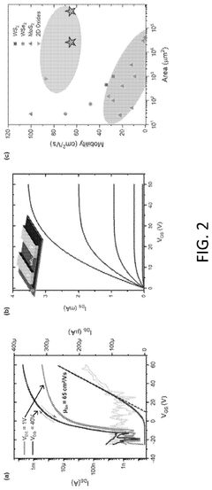
Technical Solution: The CEA has developed advanced transparent oxide semiconductor (TOS) technology for non-contact sensing applications, focusing on amorphous indium-gallium-zinc-oxide (a-IGZO) materials. Their approach involves creating high-performance TFT arrays using room-temperature deposition processes that enable integration on flexible substrates. CEA's technology utilizes specialized metal oxide compositions that achieve carrier mobilities exceeding 10 cm²/Vs while maintaining optical transparency above 80% in the visible spectrum. This enables the creation of transparent sensor arrays that can detect objects through capacitive coupling without direct contact. The CEA has demonstrated functional prototypes incorporating these transparent oxide layers in proximity detection systems, touchless interfaces, and environmental monitoring devices. Their research has shown that optimized oxide compositions can achieve detection distances up to 15cm while consuming minimal power, making them suitable for battery-operated IoT applications.
Strengths: Superior stability compared to organic alternatives; excellent optical transparency enabling integration into displays; compatibility with existing manufacturing infrastructure. Weaknesses: Higher processing temperatures than some competing technologies; potential indium supply constraints for large-scale production; sensitivity to ambient humidity requiring encapsulation.
Key Patents and Scientific Breakthroughs in Transparent Oxide Sensors
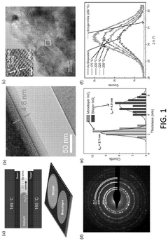
Liquid metal printed 2d ultrahigh mobility conducting oxide transistors
PatentPendingUS20240332017A1
Innovation
- A liquid metal printing method that operates at low temperatures (40° C to 450° C) to form alloyed oxide films, enabling the deposition of nanocrystalline ultrathin films with high conductivity and transparency, suitable for large-area flexible electronics, by using a dielectric and metal workpieces to form an alloyed oxide film with precise control over thickness and electronic properties.
Material Sustainability and Environmental Impact Assessment
The environmental impact of transparent oxide materials in non-contact sensor development represents a critical consideration for sustainable technology advancement. These materials, primarily including indium tin oxide (ITO), zinc oxide (ZnO), and various other metal oxides, present both environmental challenges and opportunities throughout their lifecycle.
The extraction processes for raw materials used in transparent oxides, particularly indium, involve significant environmental disruption. Mining operations contribute to habitat destruction, soil erosion, and water contamination. Additionally, the refining processes generate substantial carbon emissions and require considerable energy inputs, with some estimates suggesting that the production of high-purity indium for ITO consumes approximately 1,500-2,000 kWh per kilogram.
Manufacturing transparent oxide thin films typically employs energy-intensive physical vapor deposition or sputtering techniques, which further contribute to the carbon footprint of these materials. Chemical precursors used in certain deposition methods may contain toxic compounds that require careful handling and disposal to prevent environmental contamination.
However, the sustainability profile of transparent oxides must be evaluated against their operational benefits in non-contact sensing applications. These materials enable longer device lifespans through contactless operation, reducing the frequency of replacement and associated waste generation. Furthermore, their application in energy-efficient sensors for smart buildings and industrial monitoring can contribute to overall energy conservation that may offset initial production impacts.
Recent advancements in alternative transparent conductive materials show promising environmental improvements. Graphene-based transparent conductors and silver nanowire networks potentially offer reduced environmental impact compared to traditional oxide materials, though these alternatives currently face scalability and performance challenges in sensor applications.
End-of-life considerations for transparent oxide materials present additional environmental concerns. The recovery of indium and other valuable components from discarded devices remains technically challenging and economically marginal, resulting in significant material loss through conventional electronic waste processing.
Life cycle assessment (LCA) studies indicate that the environmental impact of transparent oxide-based sensors can be optimized through careful material selection and processing improvements. Research suggests that reducing film thickness, implementing closed-loop recycling systems, and developing lower-temperature deposition techniques could significantly decrease the environmental footprint of these materials while maintaining their functional properties in non-contact sensing applications.
Integration Challenges with Existing Sensing Platforms
The integration of transparent oxide-based non-contact sensors with existing sensing platforms presents significant technical challenges that require careful consideration. Current sensing infrastructures are predominantly designed around traditional materials and technologies, creating compatibility issues when introducing transparent oxide components. These challenges manifest across multiple dimensions including electrical interfacing, signal processing, and physical form factors.
Electrical integration poses a primary concern as transparent conducting oxides (TCOs) often exhibit different electrical characteristics compared to conventional sensor materials. The impedance matching between TCO-based sensors and existing signal conditioning circuits requires additional interface components, increasing system complexity and potentially introducing signal degradation. Furthermore, the unique capacitive and resistive properties of materials like ITO (Indium Tin Oxide) and AZO (Aluminum-doped Zinc Oxide) necessitate specialized amplification and filtering circuits that may not be readily available in standard sensing platforms.
Data processing frameworks present another integration hurdle. Existing algorithms and calibration methods are typically optimized for traditional sensor responses and may not adequately interpret the signal characteristics of transparent oxide sensors. This necessitates the development of new computational models and signal processing techniques specifically tailored to the response patterns of these novel materials, requiring significant investment in software development and validation.
Physical integration challenges also emerge when incorporating transparent oxide sensors into existing hardware. The mechanical properties of TCO films, including their brittleness and adhesion characteristics, can complicate mounting and connection to conventional sensor housings. Additionally, environmental protection requirements differ from traditional sensors, as transparent oxides may exhibit unique degradation mechanisms when exposed to humidity, temperature fluctuations, or certain chemicals present in industrial environments.
Manufacturing compatibility represents a substantial barrier to widespread integration. Current production lines for sensor assemblies are not typically equipped to handle the deposition and patterning processes required for high-quality transparent oxide films. The transition to compatible manufacturing workflows demands significant retooling and process development, increasing the economic threshold for adoption.
Standardization issues further complicate integration efforts. The lack of established industry standards for transparent oxide sensor components creates uncertainty in design specifications and performance metrics. This absence of standardization impedes interoperability with existing sensor networks and data acquisition systems, limiting the potential for seamless integration into established sensing ecosystems.
Unlock deeper insights with PatSnap Eureka Quick Research — get a full tech report to explore trends and direct your research. Try now!
Generate Your Research Report Instantly with AI Agent
Supercharge your innovation with PatSnap Eureka AI Agent Platform!