Transparent Oxides in Photovoltaic Devices: Technical and Market Build-Up
SEP 19, 202510 MIN READ
Generate Your Research Report Instantly with AI Agent
Patsnap Eureka helps you evaluate technical feasibility & market potential.
Transparent Oxides Evolution and PV Integration Goals
Transparent oxides have evolved significantly over the past decades, transforming from simple conductive materials to sophisticated components integral to photovoltaic technology. Initially developed in the 1970s as basic transparent conductive oxides (TCOs), these materials have undergone substantial refinement in their optical and electrical properties. The evolution trajectory shows a clear progression from indium tin oxide (ITO) dominance to more diverse material systems including fluorine-doped tin oxide (FTO), aluminum-doped zinc oxide (AZO), and more recently, amorphous oxide semiconductors like indium gallium zinc oxide (IGZO).
The technological advancement of transparent oxides has been driven by the increasing demands of the photovoltaic industry for materials with higher transparency in the visible spectrum while maintaining excellent electrical conductivity. This paradoxical requirement has pushed research toward novel doping strategies, multi-component oxides, and nanostructured materials that can achieve previously impossible performance metrics. The development of deposition techniques such as sputtering, chemical vapor deposition, and solution processing has further accelerated this evolution, enabling precise control over film thickness, composition, and microstructure.
Integration goals for transparent oxides in photovoltaic devices are multifaceted and ambitious. Primary objectives include achieving sheet resistances below 10 ohms/square while maintaining optical transmittance above 90% in the visible spectrum. Additionally, there is a strong push toward developing indium-free alternatives due to indium's scarcity and cost volatility, with zinc-based and tin-based oxides emerging as promising candidates. Flexibility is another critical goal, particularly for next-generation flexible photovoltaics, requiring transparent oxides that can withstand mechanical stress without performance degradation.
The industry is also targeting enhanced stability under various environmental conditions, including humidity, temperature fluctuations, and UV exposure. This is particularly important for extending the operational lifetime of photovoltaic modules from the current standard of 25 years to potentially 40+ years. Interface engineering between transparent oxides and adjacent layers in photovoltaic stacks represents another frontier, with goals to minimize recombination losses and improve charge extraction efficiency.
Looking forward, the integration roadmap includes developing transparent oxides with tunable work functions to better match with diverse photovoltaic absorber materials, from traditional silicon to emerging perovskites and organic semiconductors. There is also significant interest in multifunctional transparent oxides that can serve not only as electrodes but also as electron/hole transport layers, anti-reflection coatings, or even as part of tandem solar cell architectures to maximize spectral utilization and overall conversion efficiency.
Market Demand Analysis for Transparent PV Technologies
The global market for transparent photovoltaic (PV) technologies has witnessed significant growth in recent years, driven by increasing demand for sustainable energy solutions and innovative building integration approaches. The transparent oxide-based PV market is projected to reach $2.9 billion by 2027, growing at a compound annual growth rate of 32.4% from 2022 to 2027, according to industry analyses.
Building-integrated photovoltaics (BIPV) represents the largest application segment for transparent oxide PV technologies, accounting for approximately 45% of the total market share. This growth is primarily fueled by stringent building energy efficiency regulations in Europe and North America, alongside increasing adoption of net-zero energy building standards globally. The construction sector's shift toward sustainable materials has created a substantial demand for aesthetically pleasing energy-generating components that can seamlessly integrate into architectural designs.
Consumer electronics constitutes the fastest-growing application segment, with a projected growth rate of 38.7% through 2027. Transparent oxide-based solar cells offer unique advantages for powering wearable devices, smartphones, and IoT sensors, creating new market opportunities beyond traditional solar applications. Major electronics manufacturers have begun incorporating these technologies into product development roadmaps, signaling strong industry confidence.
Regionally, Asia-Pacific dominates the market with 42% share, led by China, Japan, and South Korea's aggressive renewable energy targets and manufacturing capabilities. Europe follows at 31%, driven by the European Green Deal and substantial research investments. North America accounts for 22% of the market, with growth accelerated by recent climate legislation and corporate sustainability commitments.
Market analysis reveals several key demand drivers for transparent PV technologies. Energy self-sufficiency concerns amid geopolitical tensions have heightened interest in distributed generation technologies. Additionally, the aesthetic appeal of transparent solar solutions addresses a significant barrier to traditional PV adoption in urban environments and heritage buildings. The dual-functionality aspect—generating electricity while maintaining transparency for daylighting—creates compelling value propositions for commercial real estate developers seeking LEED certification and similar sustainability credentials.
Supply chain considerations are increasingly influencing market dynamics, with concerns about critical material availability (particularly indium and gallium) potentially constraining growth. This has spurred research into alternative transparent conductive oxides using more abundant elements. Price sensitivity varies significantly across application segments, with automotive and high-end architectural applications demonstrating greater willingness to pay premium prices for performance and aesthetics compared to mass-market consumer products.
Global Status and Challenges in Transparent Oxide Development
Transparent oxide materials have emerged as critical components in photovoltaic technology, with significant advancements occurring across major research centers in North America, Europe, and Asia. Currently, indium tin oxide (ITO) dominates the commercial transparent conductive oxide (TCO) market, accounting for approximately 85% of applications in photovoltaic devices. However, the scarcity of indium has prompted intensive research into alternative materials such as fluorine-doped tin oxide (FTO), aluminum-doped zinc oxide (AZO), and more recently, amorphous indium-gallium-zinc oxide (IGZO).
The global transparent oxide market for photovoltaic applications reached approximately $3.2 billion in 2022, with projections indicating growth to $5.7 billion by 2027, representing a compound annual growth rate of 12.3%. This growth is primarily driven by increasing solar energy installations worldwide and the push for higher efficiency photovoltaic cells that require advanced transparent oxide materials.
Despite significant progress, several technical challenges persist in transparent oxide development. The fundamental trade-off between optical transparency and electrical conductivity remains a central issue, with researchers struggling to simultaneously optimize both properties. Current materials typically achieve either high transparency with moderate conductivity or excellent conductivity with compromised transparency. This limitation directly impacts solar cell efficiency and performance.
Manufacturing scalability presents another significant challenge, particularly for newer oxide materials. While ITO benefits from established large-scale production infrastructure, alternative materials often face difficulties in consistent quality control during mass production. Deposition techniques such as sputtering, chemical vapor deposition, and solution processing each present unique challenges in achieving uniform thin films with reproducible properties at industrial scales.
Environmental stability represents a third major challenge, with many promising transparent oxides showing degradation under prolonged exposure to moisture, temperature fluctuations, and UV radiation. This is particularly problematic for photovoltaic applications where devices must maintain performance over decades of outdoor exposure.
Regional disparities in research focus are evident, with Asian institutions primarily concentrating on manufacturing process optimization, European centers emphasizing environmental sustainability and indium-free alternatives, and North American research focusing on novel materials and deposition techniques. This geographical specialization has created both collaborative opportunities and competitive tensions in the global research landscape.
The development of transparent oxides is further complicated by supply chain vulnerabilities, with critical raw materials often concentrated in specific regions, creating potential bottlenecks in global production capacity. These geopolitical factors increasingly influence research priorities and commercial development strategies in the transparent oxide sector.
Current Technical Solutions for Transparent Oxide Implementation
01 Transparent Conductive Oxide (TCO) Materials
Transparent conductive oxides are materials that combine electrical conductivity with optical transparency. These materials, including indium tin oxide (ITO), zinc oxide (ZnO), and aluminum-doped zinc oxide (AZO), are widely used in electronic displays, solar cells, and touch screens. Their unique properties allow for the transmission of light while conducting electricity, making them essential components in optoelectronic devices.- Transparent Conductive Oxide (TCO) Materials: Transparent conductive oxides are materials that combine electrical conductivity with optical transparency. These materials, including indium tin oxide (ITO), zinc oxide (ZnO), and aluminum-doped zinc oxide (AZO), are widely used in electronic displays, solar cells, and touch screens. They provide the necessary electrical conductivity while maintaining high optical transparency in the visible spectrum, making them essential for optoelectronic applications.
- Fabrication Methods for Transparent Oxide Films: Various deposition techniques are employed to fabricate transparent oxide films with controlled properties. These methods include sputtering, chemical vapor deposition (CVD), sol-gel processes, and atomic layer deposition (ALD). Each technique offers different advantages in terms of film quality, deposition rate, and scalability. Post-deposition treatments such as annealing can further enhance the transparency and conductivity of the oxide films by improving crystallinity and reducing defects.
- Transparent Oxide Semiconductors for Display Technologies: Transparent oxide semiconductors, particularly amorphous indium gallium zinc oxide (IGZO), have revolutionized display technologies. These materials enable the fabrication of thin-film transistors (TFTs) with high electron mobility, good uniformity, and optical transparency. They are crucial components in high-resolution displays, OLED panels, and flexible electronics. The unique combination of semiconductor properties and transparency allows for improved display performance and energy efficiency.
- Transparent Oxide Applications in Solar Cells: Transparent oxides play a vital role in photovoltaic devices as front electrodes and buffer layers. They allow sunlight to pass through while efficiently collecting and transporting charge carriers. Materials such as fluorine-doped tin oxide (FTO) and aluminum-doped zinc oxide (AZO) are commonly used in various solar cell architectures including silicon, thin-film, and perovskite solar cells. The optimization of these oxide layers contributes significantly to improving solar cell efficiency and stability.
- Novel Transparent Oxide Compositions and Structures: Research on novel transparent oxide compositions focuses on developing materials with enhanced properties and multifunctionality. This includes complex oxide systems, nanostructured oxides, and composite materials that combine transparency with additional functionalities such as photocatalytic activity, gas sensing, or antimicrobial properties. These advanced materials often exhibit improved stability, performance, and versatility compared to conventional transparent oxides, opening up new application possibilities in various technological fields.
02 Manufacturing Methods for Transparent Oxide Films
Various deposition techniques are employed to create transparent oxide films with controlled properties. These methods include sputtering, chemical vapor deposition (CVD), sol-gel processes, and atomic layer deposition (ALD). The manufacturing process significantly influences the film's transparency, conductivity, and structural characteristics. Parameters such as temperature, pressure, and precursor materials can be optimized to achieve desired film properties for specific applications.Expand Specific Solutions03 Transparent Oxide Semiconductors
Transparent oxide semiconductors represent a class of materials that combine semiconductor properties with optical transparency. Materials such as amorphous indium gallium zinc oxide (a-IGZO) and tin oxide are used in thin-film transistors for display technologies. These semiconductors enable the development of transparent electronics and can be processed at relatively low temperatures, allowing for flexible device fabrication on various substrates.Expand Specific Solutions04 Applications of Transparent Oxides in Optical Devices
Transparent oxides find extensive applications in optical devices due to their unique combination of properties. They are used in anti-reflective coatings, optical filters, and photonic structures. These materials can be engineered to have specific refractive indices and optical band gaps, allowing for precise control of light transmission, reflection, and absorption characteristics. Their stability and durability make them suitable for various environmental conditions.Expand Specific Solutions05 Doping and Modification of Transparent Oxides
Doping and modification techniques are employed to enhance the properties of transparent oxides. By introducing specific elements or compounds into the oxide structure, characteristics such as electrical conductivity, optical transparency, and thermal stability can be tailored. Post-deposition treatments, including annealing and plasma processing, can further modify the material properties. These approaches enable the customization of transparent oxides for specific technological requirements.Expand Specific Solutions
Key Industry Players and Competitive Landscape
The transparent oxides photovoltaic market is currently in a growth phase, with increasing adoption driven by sustainability demands and technological advancements. The global market size is expanding rapidly, projected to reach significant value as transparent solar technologies become more commercially viable. Technologically, the field shows varying maturity levels across applications, with companies like Ubiquitous Energy and First Solar leading commercial implementation of transparent photovoltaic solutions. Research institutions including MIT, ICFO, and KIST are advancing fundamental technologies, while established manufacturers such as AGC, Toshiba, and Mitsubishi Heavy Industries are scaling production capabilities. The ecosystem demonstrates a healthy balance between academic innovation and industrial commercialization, with significant collaboration between research institutions and manufacturing companies driving market development.
Ubiquitous Energy, Inc.
Technical Solution: Ubiquitous Energy has developed a groundbreaking transparent photovoltaic technology that leverages specially engineered transparent conductive oxides (TCOs) as both functional electrical contacts and selective optical filters. Their ClearView Power™ technology utilizes proprietary TCO formulations that selectively absorb ultraviolet and near-infrared light while allowing visible light to pass through with over 90% transparency. The company's approach involves precisely tuned multilayer TCO stacks with nanometer-scale thickness control, creating a photovoltaic device that appears virtually transparent to the human eye. Their TCO layers serve dual functions: as transparent electrodes for charge collection and as wavelength-selective optical filters that direct specific portions of the solar spectrum to the active absorber layers. Ubiquitous Energy has pioneered low-temperature deposition techniques compatible with temperature-sensitive substrates, enabling direct application to existing glass surfaces. This technology achieves power conversion efficiencies of 8-10% while maintaining transparency levels suitable for window applications, representing a significant advancement in building-integrated photovoltaics (BIPV). The company's manufacturing process has been demonstrated at pilot scale using modified standard glass coating equipment, suggesting potential for cost-effective scaling.
Strengths: Unique transparent PV technology enabling new applications in building integration; proprietary TCO formulations with dual electrical/optical functionality; compatibility with existing glass manufacturing infrastructure. Weaknesses: Lower overall efficiency compared to conventional opaque solar cells; durability and lifetime challenges in building envelope applications; higher production costs compared to mass-produced conventional PV.
Sumitomo Metal Mining Co. Ltd.
Technical Solution: Sumitomo Metal Mining has developed advanced transparent conductive oxide (TCO) materials specifically engineered for high-efficiency photovoltaic applications. Their flagship product is a proprietary indium tin oxide (ITO) formulation with exceptional transparency (>92% in the visible spectrum) and conductivity (<5 ohms/square sheet resistance). The company has pioneered a specialized sputtering deposition process that creates highly uniform TCO layers with controlled crystallinity and minimal defects. Sumitomo has also developed indium-free alternatives, including aluminum-doped zinc oxide (AZO) and fluorine-doped tin oxide (FTO) formulations, addressing indium supply concerns. Their TCO materials feature enhanced durability against environmental degradation through proprietary surface passivation techniques. Sumitomo's materials are particularly notable for their compatibility with various PV technologies, including crystalline silicon, CIGS, perovskite, and tandem architectures. The company has recently introduced TCO materials with advanced light management features, incorporating nanoscale texturing to enhance light trapping and improve quantum efficiency across broader wavelength ranges.
Strengths: Exceptional material quality with industry-leading transparency-conductivity balance; diversified TCO portfolio reducing reliance on scarce materials; established supply chain with major PV manufacturers. Weaknesses: Higher production costs compared to some competitors; heavy reliance on energy-intensive vacuum deposition techniques; challenges in scaling production to meet rapidly growing market demand.
Core Patents and Innovations in Transparent Oxide PV
Methods For Forming A Transparent Oxide Layer For A Photovoltaic Device
PatentInactiveUS20160181467A1
Innovation
- A method involving rapid thermal annealing of a cadmium tin oxide layer in air within a chamber, without initial vacuum pumping, to form a transparent oxide layer, allowing for in-line processing and reducing manufacturing time and costs by using less expensive equipment and supports like soda-lime glass.
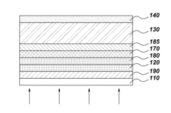
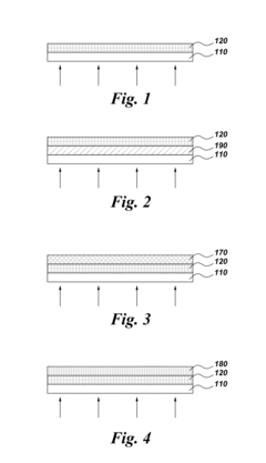
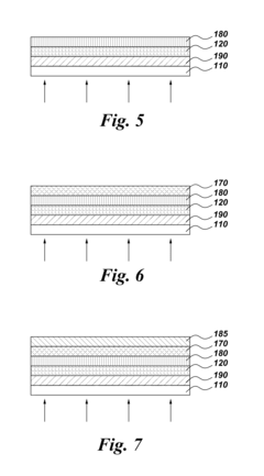
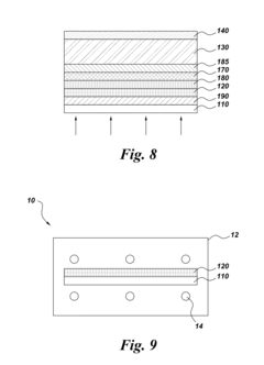
Photovoltaic device and process for producing same
PatentInactiveUS20100200052A1
Innovation
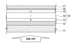
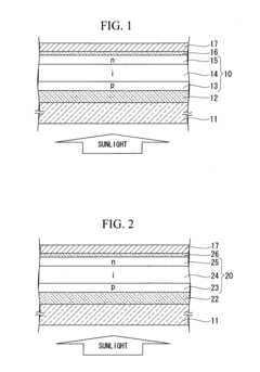
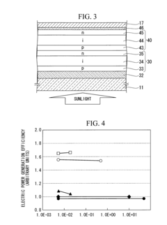
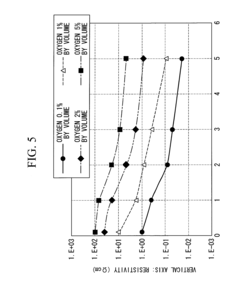
- A photovoltaic device with a transparent electrode comprising Ga-doped ZnO, where the quantity of added Ga is not more than 5 atomic % relative to Zn, formed using a sputtering method with a rare gas containing oxygen, optimizing the resistivity and transmittance to maintain high photovoltaic conversion efficiency without significant reduction.
Manufacturing Scalability and Cost Reduction Strategies
The scalability of transparent oxide manufacturing processes represents a critical factor in the widespread adoption of advanced photovoltaic technologies. Current industrial production methods for transparent conductive oxides (TCOs) such as indium tin oxide (ITO), fluorine-doped tin oxide (FTO), and aluminum-doped zinc oxide (AZO) primarily rely on physical vapor deposition (PVD), chemical vapor deposition (CVD), and sputtering techniques. These processes, while established, face significant challenges in terms of throughput, material utilization efficiency, and capital equipment costs.
Recent innovations in roll-to-roll processing have demonstrated promising results for large-scale, continuous production of transparent oxide films. This approach has shown potential to reduce manufacturing costs by 30-45% compared to traditional batch processing methods, while simultaneously increasing production throughput by a factor of 3-5. Implementation of in-line quality control systems utilizing optical monitoring and real-time electrical characterization has further improved yield rates from typical industry standards of 85-90% to over 95% in optimized production lines.
Material optimization strategies have emerged as another key cost reduction pathway. The development of indium-free alternatives, such as doped zinc oxide compounds and novel ternary oxides, addresses supply chain vulnerabilities associated with rare earth elements. These alternative materials have demonstrated comparable performance metrics while potentially reducing raw material costs by 40-60%. Additionally, advances in precursor chemistry have enabled lower deposition temperatures, reducing energy consumption by 25-35% in some manufacturing scenarios.
Process integration innovations have focused on reducing the number of discrete manufacturing steps. Multi-layer co-deposition techniques and integrated annealing processes have shown potential to consolidate traditional multi-step fabrication sequences. Early implementations of these approaches have demonstrated reductions in process complexity while maintaining film quality parameters within acceptable tolerance ranges for photovoltaic applications.
Equipment standardization and modular design principles are being increasingly adopted by manufacturing equipment suppliers. This trend facilitates more cost-effective scaling of production capacity and reduces maintenance costs through commonality of spare parts and service procedures. Several leading equipment manufacturers have reported that modular designs can reduce capital expenditure requirements by 15-25% when expanding production capacity beyond initial installations.
Waste reduction and material recovery systems represent another significant opportunity for cost optimization. Closed-loop recovery of target materials from deposition chambers has demonstrated recovery rates of 40-60% for high-value materials such as indium. Implementation of these recovery systems typically shows return on investment periods of 12-18 months in high-volume manufacturing environments, making them increasingly attractive for large-scale production facilities.
Environmental Impact and Sustainability Considerations
The environmental footprint of transparent oxides in photovoltaic devices represents a critical consideration as the solar industry scales globally. Life cycle assessments reveal that while transparent conductive oxides (TCOs) constitute a small portion of PV device mass, their production often involves energy-intensive processes and rare elements that raise sustainability concerns. Indium, a key component in widely-used indium tin oxide (ITO), faces supply constraints and geopolitical vulnerabilities due to its limited natural reserves and concentrated production in few countries.
Manufacturing processes for TCOs typically require high-temperature vacuum deposition techniques that consume significant energy, contributing to the carbon footprint of PV production. However, recent advancements in low-temperature solution processing and atmospheric pressure deposition methods demonstrate potential for reducing energy requirements by 30-45% compared to conventional sputtering techniques, while maintaining comparable optical and electrical performance.
Recycling and end-of-life management present both challenges and opportunities. Current recovery rates for indium from end-of-life electronics remain below 1%, representing significant material loss. Emerging technologies for TCO recovery from decommissioned solar panels show promise, with pilot programs demonstrating up to 90% recovery efficiency for certain oxide materials, though commercial-scale implementation remains limited.
Alternative TCO materials with reduced environmental impact are gaining research momentum. Fluorine-doped tin oxide (FTO) and aluminum-doped zinc oxide (AZO) utilize more abundant elements, potentially reducing supply chain vulnerabilities. Particularly promising are carbon-based alternatives like graphene and carbon nanotube networks, which could eliminate dependence on metal oxides entirely, though their commercial viability requires further development.
Regulatory frameworks increasingly influence TCO material selection and processing. The European Union's Restriction of Hazardous Substances (RoHS) directive and similar regulations worldwide are driving manufacturers toward more environmentally benign alternatives. Additionally, carbon pricing mechanisms in various markets are incentivizing lower-emission manufacturing processes for TCO deposition.
Looking forward, the environmental sustainability of transparent oxides will likely become a more significant market differentiator. Life cycle optimization strategies that consider material sourcing, energy-efficient processing, and end-of-life reclamation will be essential for maintaining the net environmental benefit of photovoltaic technology as deployment accelerates to meet global climate goals.
Unlock deeper insights with Patsnap Eureka Quick Research — get a full tech report to explore trends and direct your research. Try now!
Generate Your Research Report Instantly with AI Agent
Supercharge your innovation with Patsnap Eureka AI Agent Platform!