

Deploying ICP-MS for Semiconductor Industry: Calibration Techniques
SEP 19, 20259 MIN READ
Generate Your Research Report Instantly with AI Agent
PatSnap Eureka helps you evaluate technical feasibility & market potential.
ICP-MS Technology Evolution in Semiconductor Manufacturing
Inductively Coupled Plasma Mass Spectrometry (ICP-MS) has undergone significant evolution since its introduction to semiconductor manufacturing in the late 1980s. Initially developed for geological and environmental analysis, the technology was adapted for semiconductor applications due to its exceptional sensitivity for detecting trace elements at parts-per-trillion levels, which became increasingly critical as semiconductor feature sizes shrank below the micron scale.
The first generation of ICP-MS systems used in semiconductor manufacturing (1990s) featured quadrupole mass analyzers with relatively simple sample introduction systems. These early systems provided detection limits in the parts-per-billion range but suffered from numerous matrix interferences and limited dynamic range. The primary calibration techniques relied on external standards, which often proved inadequate for the complex matrices encountered in semiconductor processing.
By the early 2000s, the second generation emerged with collision/reaction cell technology, representing a pivotal advancement in ICP-MS evolution. These systems effectively reduced polyatomic interferences through ion-molecule reactions, dramatically improving detection capabilities for critical elements like iron, potassium, and calcium in silicon matrices. Calibration techniques evolved to include internal standardization methods, significantly enhancing measurement accuracy.
The third generation (mid-2000s to early 2010s) introduced high-resolution sector-field ICP-MS systems capable of resolving spectral interferences through superior mass resolution rather than chemical reactions. This development enabled more precise analysis of ultra-pure semiconductor materials and process chemicals. During this period, isotope dilution calibration techniques gained prominence, offering unprecedented accuracy for quantifying contaminants.
The current generation of ICP-MS technology (2010s-present) features triple-quadrupole systems that combine collision/reaction cell technology with additional quadrupole filtering. These systems provide exceptional sensitivity and selectivity for semiconductor applications. Modern calibration approaches now incorporate matrix-matched standards and automated standard addition techniques, addressing the complex matrices encountered in advanced semiconductor processes.
Recent innovations include specialized sample introduction systems designed specifically for semiconductor applications, such as vapor generation techniques for volatile elements and laser ablation systems for direct solid sampling. These developments have expanded ICP-MS applications beyond traditional liquid sample analysis to include surface contamination monitoring and depth profiling of semiconductor materials.
The integration of ICP-MS with automated sample preparation systems and sophisticated data processing algorithms represents the latest evolutionary step, enabling high-throughput analysis essential for modern semiconductor manufacturing environments. Machine learning algorithms are increasingly being applied to calibration procedures, allowing for adaptive calibration models that compensate for matrix effects and instrument drift in real-time.
Market Demand for High-Precision Trace Element Analysis
The semiconductor industry's demand for high-precision trace element analysis has experienced exponential growth over the past decade, driven primarily by the continuous miniaturization of integrated circuits and increasingly stringent quality control requirements. As semiconductor device dimensions shrink below 5nm, even trace contaminants at parts-per-trillion (ppt) levels can significantly impact device performance and yield. This has created an urgent market need for advanced analytical techniques like Inductively Coupled Plasma Mass Spectrometry (ICP-MS) with enhanced calibration capabilities.
Market research indicates that the global semiconductor process control equipment market, which includes high-precision analytical instruments, reached approximately $7.2 billion in 2022 and is projected to grow at a compound annual growth rate of 8.3% through 2028. Within this segment, the demand for trace element analysis solutions is growing at an even faster rate of 11.2% annually, reflecting the critical importance of contamination control in advanced semiconductor manufacturing.
Leading semiconductor manufacturers have significantly increased their investment in analytical capabilities, with major players like TSMC, Samsung, and Intel collectively spending over $900 million on advanced metrology and analytical equipment in 2022 alone. Industry surveys reveal that 78% of semiconductor manufacturers consider trace element analysis as "critical" or "very important" to their quality control processes.
The demand is particularly strong in regions with concentrated semiconductor manufacturing capacity, with East Asia accounting for 63% of the global market for high-precision analytical instruments. North America follows at 21%, with Europe representing 14% of the market. The fastest growth is observed in emerging semiconductor manufacturing hubs in Southeast Asia and India.
Beyond traditional semiconductor applications, emerging technologies such as quantum computing, advanced packaging, and wide-bandgap semiconductors are creating new requirements for trace element analysis. These applications often demand even lower detection limits and higher precision than conventional silicon-based semiconductor manufacturing.
Customer requirements have evolved significantly, with semiconductor manufacturers now demanding not just lower detection limits but also faster analysis times, higher throughput, and more robust calibration techniques. The ability to perform in-line or at-line measurements rather than laboratory-based analysis is increasingly valued, with 67% of manufacturers expressing interest in solutions that can be integrated directly into their production workflows.
The market also shows strong demand for comprehensive software solutions that can integrate analytical data with manufacturing execution systems and provide advanced statistical process control capabilities. This reflects the industry's move toward more data-driven manufacturing approaches and the implementation of Industry 4.0 principles in semiconductor fabrication facilities.
Current Challenges in ICP-MS Semiconductor Applications
Despite the significant advancements in ICP-MS technology for semiconductor applications, several critical challenges persist that limit its full potential in this highly demanding industry. The ultra-trace detection requirements of modern semiconductor manufacturing processes, which now operate at sub-10nm nodes, demand unprecedented analytical precision that pushes current ICP-MS systems to their limits. Contamination control during sample preparation and analysis remains one of the most significant hurdles, as even minimal environmental interference can compromise results.
Matrix effects present a substantial challenge unique to semiconductor samples, where complex chemical compositions can cause signal suppression or enhancement, leading to inaccurate quantification. The high-purity acids and reagents used in semiconductor processing create difficult analytical matrices that require specialized calibration approaches beyond standard methods.
Instrument stability issues are particularly problematic for semiconductor applications, where long-term reproducibility is essential for process control. Drift in mass calibration, detector response, and plasma conditions can introduce significant errors in measurements conducted over extended production monitoring periods.
The semiconductor industry's need for multi-element analysis at varying concentration ranges simultaneously presents another technical barrier. Current systems struggle to maintain linearity across the ultra-trace to trace concentration ranges required for different elements in the same sample, necessitating complex calibration strategies.
Sample introduction efficiency remains suboptimal, with typical nebulizer systems delivering only 1-2% of the sample to the plasma. This limitation is particularly problematic when sample volumes are restricted, as is common with expensive semiconductor materials and process chemicals.
Memory effects between samples pose significant challenges, especially when analyzing elements that tend to adhere to sample introduction components. These carryover issues can create false positives that are unacceptable in an industry where decisions about batch acceptance are made based on parts-per-trillion measurements.
Calibration reference materials specifically designed for semiconductor matrices are limited in availability and scope. The lack of certified reference materials that accurately represent the complex matrices encountered in semiconductor processing hampers method validation and inter-laboratory comparability.
Automation and integration challenges persist as semiconductor fabs move toward fully automated analytical workflows. Current ICP-MS systems often require significant customization to interface with fab-wide information systems and automated sample handling infrastructure, creating implementation barriers.
State-of-the-Art Calibration Methods for Semiconductor Analysis
01 External Calibration Methods for ICP-MS
External calibration is a fundamental technique for ICP-MS analysis that involves preparing a series of standard solutions with known concentrations of target elements. These standards are used to create calibration curves that establish the relationship between instrument response and analyte concentration. This method typically includes blank solutions for background correction and requires careful preparation of standards that match the matrix of the samples being analyzed to minimize matrix effects. External calibration provides reliable quantitative results when matrix matching is properly implemented.- External Calibration Methods for ICP-MS: External calibration is a fundamental technique for ICP-MS analysis that involves creating a calibration curve using standard solutions of known concentrations. This method establishes a relationship between analyte concentration and instrument response. The calibration standards typically cover the expected concentration range of the samples being analyzed. This approach provides accurate quantification when matrix effects are minimal or when matrix-matched standards are used.
- Internal Standard Calibration for ICP-MS: Internal standard calibration involves adding known concentrations of elements not present in the sample to both standards and unknowns. These internal standards compensate for matrix effects, instrument drift, and other variations during analysis. Ideal internal standards have similar mass and ionization potential to the analytes of interest. This technique improves precision and accuracy, especially for complex matrices or long analytical runs.
- Isotope Dilution Mass Spectrometry (IDMS) for ICP-MS: Isotope dilution is a high-precision calibration technique that involves adding an enriched isotope of the element of interest to the sample. By measuring the altered isotope ratio after equilibration, accurate quantification can be achieved independent of matrix effects or incomplete analyte recovery. This method is considered a primary method of measurement with potentially the lowest uncertainty, though it requires elements with multiple stable isotopes and specialized reference materials.
- Standard Addition Calibration for Complex Matrices: Standard addition calibration involves adding increasing amounts of analyte to aliquots of the sample. This technique is particularly useful for complex or variable matrices where matrix-matching is difficult. By plotting the instrument response against the added concentration and extrapolating to zero addition, the original analyte concentration can be determined. This method effectively compensates for matrix effects but requires more sample volume and preparation time.
- Automated Calibration Systems and Quality Control: Automated calibration systems for ICP-MS incorporate hardware and software solutions to streamline the calibration process. These systems may include auto-diluters, automated standard preparation, and quality control measures such as calibration verification standards and drift correction. Continuous monitoring of instrument performance using check standards ensures data quality throughout analytical runs. Advanced systems may incorporate machine learning algorithms to optimize calibration parameters and detect anomalies.
02 Internal Standard Calibration Techniques
Internal standard calibration involves adding known concentrations of reference elements to both samples and calibration standards to compensate for matrix effects, instrument drift, and signal fluctuations during ICP-MS analysis. The internal standards selected typically have similar ionization potentials and masses to the target analytes but are not present in the original samples. By monitoring the ratio of analyte signal to internal standard signal, this method improves measurement precision and accuracy, particularly for complex matrices or long analytical sequences where instrument performance may vary over time.Expand Specific Solutions03 Standard Addition Calibration for Complex Matrices
Standard addition calibration is particularly useful for analyzing complex or unknown sample matrices in ICP-MS where matrix effects cannot be easily matched using external calibration. This technique involves adding increasing amounts of analyte standards directly to aliquots of the sample, creating a calibration curve specific to each sample's matrix. By extrapolating the curve to zero standard addition, the original analyte concentration can be determined accurately. This method effectively compensates for matrix-induced signal suppression or enhancement without requiring complete characterization of the sample matrix.Expand Specific Solutions04 Isotope Dilution Mass Spectrometry Calibration
Isotope dilution mass spectrometry (IDMS) is a high-precision calibration technique for ICP-MS that involves adding isotopically enriched standards to samples. By measuring the altered isotope ratios after equilibration, precise quantification can be achieved independent of signal suppression, instrument drift, or incomplete analyte recovery. This technique is considered a primary method of measurement with potentially lower uncertainty than other calibration approaches. IDMS is particularly valuable for reference material certification and applications requiring the highest analytical accuracy, though it requires that the element of interest has at least two stable isotopes.Expand Specific Solutions05 Automated Calibration Systems and Quality Control
Advanced ICP-MS systems incorporate automated calibration procedures and quality control measures to ensure reliable analytical results. These systems may include automated standard preparation, intelligent calibration verification, real-time drift correction, and integrated quality control checks. Automated systems can perform periodic recalibration, analyze quality control samples at predetermined intervals, and apply correction algorithms to maintain calibration stability throughout analytical runs. These approaches improve laboratory efficiency, reduce human error, and provide consistent data quality by continuously monitoring and adjusting for variations in instrument performance.Expand Specific Solutions
Leading ICP-MS Equipment Manufacturers and Service Providers
The ICP-MS calibration techniques for semiconductor industry are evolving in a rapidly growing market, currently in the early maturity phase. The global semiconductor metrology market is expanding significantly as chip manufacturing processes require increasingly precise contamination control. Applied Materials, TSMC, and Intel lead in developing advanced ICP-MS calibration solutions, with specialized companies like Metara and Agilent Technologies offering complementary expertise. GLOBALFOUNDRIES and SK hynix are advancing calibration techniques for specific manufacturing processes, while research institutions like Industrial Technology Research Institute collaborate with industry players to standardize methodologies. The technology is approaching maturity but continues to evolve as semiconductor nodes shrink, requiring ever more sensitive detection limits and calibration accuracy.
Applied Materials, Inc.
Technical Solution: Applied Materials has developed proprietary ICP-MS calibration techniques integrated directly into their semiconductor manufacturing equipment, creating in-line monitoring capabilities. Their approach focuses on real-time calibration verification during wafer processing, utilizing automated standard addition methods that can be performed without interrupting production flows[1]. The company's UltraClean Technology platform incorporates specialized calibration protocols that account for matrix-specific challenges in semiconductor materials, particularly for monitoring ultra-trace metal contamination on wafer surfaces. Their calibration system employs multi-point dynamic reaction cell technology to eliminate interferences specific to semiconductor matrices while maintaining sensitivity[3]. Applied Materials has also pioneered the integration of machine learning algorithms that continuously optimize calibration parameters based on historical data patterns, allowing predictive maintenance of calibration before drift becomes significant. Their system includes specialized calibration for both bulk and surface analysis, critical for different stages of semiconductor manufacturing.
Strengths: Seamless integration with existing semiconductor manufacturing equipment; real-time calibration verification without production interruption; specialized surface and bulk analysis capabilities. Weaknesses: Requires integration with Applied Materials equipment ecosystem; higher complexity for initial setup and validation; calibration protocols may need frequent updates with process changes.
Agilent Technologies, Inc.
Technical Solution: Agilent Technologies has developed advanced ICP-MS calibration techniques specifically for semiconductor manufacturing, featuring their ICP-QQQ (triple quadrupole) technology. Their solution includes automated multi-element calibration systems with pre-configured semiconductor-specific protocols that address matrix effects common in semiconductor samples. The system employs reaction/collision cell technology to eliminate polyatomic interferences that are particularly problematic when measuring trace metals in silicon and other semiconductor materials[1]. Agilent's calibration approach incorporates internal standardization with isotope dilution techniques for highest accuracy, and their software includes semiconductor-specific quality control protocols that automatically flag deviations from expected calibration curves. Their latest systems feature automated intelligent calibration verification that can detect and correct for drift during long analytical runs, essential for high-throughput semiconductor manufacturing environments[3].
Strengths: Superior interference management through triple quadrupole technology; comprehensive semiconductor-specific calibration protocols; excellent detection limits (ppt range) for critical metals. Weaknesses: Higher initial investment compared to single-quadrupole systems; requires more specialized operator training; calibration procedures can be time-consuming for full multi-element analysis.
Critical Patents and Research in ICP-MS Calibration Technology
Inductively coupled plasma mass spectrometry
PatentInactiveJP2020027038A
Innovation
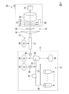
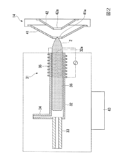
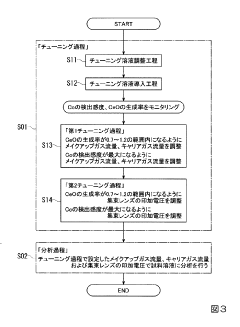
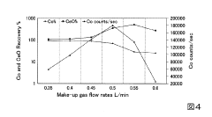
- The method involves tuning the ICP-MS system using a sample solution with a high-concentration acid matrix as a tuning liquid, adjusting carrier gas flow rates and focusing lens settings to control the production rate of coexisting element oxides within a specific range, thereby maximizing detection sensitivity.
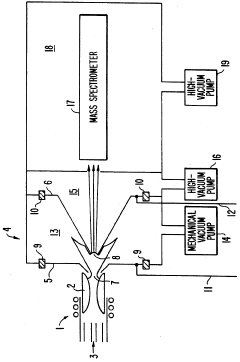
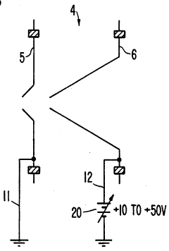
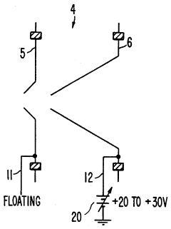
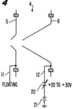
Plasma sampling interface for inductively coupled plasma-mass spectrometry (ICP-MS)
PatentInactiveUS5218204A
Innovation
- A plasma sampling interface with insulating spacers and an adjustable DC bias voltage source applying a DC bias voltage of 10 to 50 V to the skimmer, allowing the sampler to float or grounding it, enhances ion transmission by using a DC offset voltage for mass spectrometers requiring higher initial ion energy.
Cleanroom Integration Requirements for ICP-MS Systems
Integrating ICP-MS systems into semiconductor manufacturing environments requires adherence to stringent cleanroom specifications. These facilities typically operate at ISO Class 5 (Class 100) or cleaner, with controlled particle counts, temperature, humidity, and pressure differentials. The ICP-MS instrument itself generates particles and heat during operation, potentially compromising cleanroom integrity if not properly managed.
Primary integration challenges include minimizing particle generation from moving components, managing exhaust from plasma generation, and controlling electromagnetic interference that could affect sensitive semiconductor equipment. Manufacturers must implement specialized enclosures with HEPA or ULPA filtration systems to isolate the ICP-MS system while maintaining analytical performance.
Temperature stability requirements are particularly demanding, as fluctuations can affect both the cleanroom environment and instrument calibration accuracy. Most semiconductor facilities maintain temperature variations within ±0.5°C, necessitating dedicated cooling systems for ICP-MS instruments that generate significant heat during operation.
Vibration isolation represents another critical consideration, as mechanical vibrations from vacuum pumps and other ICP-MS components can propagate through cleanroom floors, potentially affecting nearby lithography or metrology equipment. Implementation of vibration dampening platforms and strategic placement within the facility layout becomes essential.
Facility modifications typically include dedicated exhaust systems for plasma gases, reinforced flooring to support the instrument weight, specialized power conditioning to prevent electrical noise, and often separate ante-rooms for sample preparation to prevent contamination. These modifications must comply with both semiconductor industry standards and safety regulations for handling the argon gas and acids used in ICP-MS analysis.
Remote operation capabilities are increasingly important, allowing technicians to control the instrument from outside the cleanroom environment, thereby reducing personnel movement and associated contamination risks. Modern ICP-MS systems designed for semiconductor applications incorporate network interfaces that enable integration with factory automation systems and manufacturing execution systems (MES).
Material compatibility presents ongoing challenges, as all components entering the cleanroom must be constructed from non-shedding, low-outgassing materials that won't introduce molecular contamination. This extends to the ICP-MS system's external housing, gas lines, and even maintenance tools, often requiring specialized versions of standard equipment.
Regulatory Compliance for Trace Metal Analysis in Semiconductors
Regulatory compliance in trace metal analysis for the semiconductor industry represents a critical framework that manufacturers must navigate to ensure product quality, safety, and market access. The semiconductor industry faces increasingly stringent regulations worldwide due to the potential environmental and health impacts of trace metals used in manufacturing processes.
The primary regulatory bodies governing trace metal analysis in semiconductors include the International Organization for Standardization (ISO), particularly ISO 14644 for cleanroom standards, and the Semiconductor Equipment and Materials International (SEMI) organization, which establishes globally recognized standards for semiconductor manufacturing. Additionally, regional regulations such as the European Union's Restriction of Hazardous Substances (RoHS) Directive and Registration, Evaluation, Authorization, and Restriction of Chemicals (REACH) impose specific limitations on trace metal content.
When deploying ICP-MS for semiconductor analysis, calibration techniques must align with these regulatory frameworks. The SEMI F57 standard specifically addresses trace metal analysis in semiconductor-grade chemicals, requiring detection limits in the parts-per-trillion (ppt) range for critical elements. This necessitates highly accurate calibration procedures that can be validated against certified reference materials (CRMs).
Compliance documentation represents another crucial aspect of regulatory adherence. Manufacturers must maintain comprehensive records of calibration procedures, including calibration curves, quality control samples, and method validation data. These records are subject to audit by regulatory authorities and must demonstrate traceability to national or international standards.
The implementation of Good Laboratory Practices (GLP) and Good Manufacturing Practices (GMP) further supports regulatory compliance in trace metal analysis. These frameworks ensure consistent application of validated analytical methods and proper documentation of all analytical procedures, including ICP-MS calibration techniques.
Emerging regulations are increasingly focusing on ultra-trace contaminants as semiconductor technology advances toward smaller node sizes. The International Technology Roadmap for Semiconductors (ITRS) continues to reduce acceptable contamination levels, driving the need for more sensitive and accurate calibration techniques in ICP-MS analysis.
Cross-border compliance presents additional challenges for semiconductor manufacturers operating globally. Different regions may have varying requirements for trace metal analysis, necessitating flexible calibration approaches that can meet the most stringent standards across all markets where products are sold.
Unlock deeper insights with PatSnap Eureka Quick Research — get a full tech report to explore trends and direct your research. Try now!
Generate Your Research Report Instantly with AI Agent
Supercharge your innovation with PatSnap Eureka AI Agent Platform!