DIW For Flexible Electronics: Conductive Ceramic-Polymer Inks
SEP 3, 202510 MIN READ
Generate Your Research Report Instantly with AI Agent
Patsnap Eureka helps you evaluate technical feasibility & market potential.
Flexible Electronics Conductive Inks Background and Objectives
Flexible electronics represent a revolutionary shift in electronic device design, enabling the creation of bendable, stretchable, and conformable electronic systems that can adapt to various surfaces and maintain functionality under mechanical deformation. The evolution of this technology has progressed significantly over the past two decades, transitioning from rigid circuit boards to malleable electronic components that can be integrated into clothing, biomedical devices, and consumer electronics.
Direct Ink Writing (DIW) has emerged as a pivotal manufacturing technique in this domain, offering precise deposition of functional materials through a computer-controlled dispensing system. The integration of DIW with conductive ceramic-polymer inks represents a particularly promising approach for fabricating flexible electronic circuits and components with enhanced electrical and mechanical properties.
Historically, flexible electronics relied heavily on metallic conductors such as silver and copper, which often faced challenges related to mechanical durability during repeated bending cycles. The introduction of ceramic materials into polymer matrices has created a new class of composite inks that combine the electrical conductivity of ceramics with the flexibility and processability of polymers, addressing many limitations of traditional materials.
The technological trajectory indicates a growing emphasis on multifunctional materials that can simultaneously provide electrical conductivity, mechanical flexibility, and additional properties such as thermal stability or biocompatibility. This evolution is driven by the increasing demand for wearable technology, Internet of Things (IoT) devices, and advanced healthcare monitoring systems that require robust yet flexible electronic components.
The primary technical objectives for conductive ceramic-polymer inks in DIW applications include achieving high electrical conductivity (>1000 S/cm), maintaining performance under mechanical strain (>1000 bending cycles without significant degradation), ensuring compatibility with various substrate materials, and developing formulations that can be processed at low temperatures (<150°C) to enable integration with temperature-sensitive components.
Current research is focused on optimizing ink rheology for precise extrusion, enhancing the interface between ceramic particles and polymer matrices to improve electrical pathways, and developing post-processing techniques that can maximize conductivity while preserving flexibility. Additionally, there is significant interest in environmentally sustainable formulations that reduce reliance on rare or toxic materials.
The convergence of nanotechnology, materials science, and additive manufacturing techniques is expected to accelerate innovation in this field, potentially leading to breakthroughs in energy storage devices, flexible displays, and soft robotics. As these technologies mature, the market for flexible electronics is projected to expand substantially, creating new opportunities for applications that were previously constrained by the rigidity of conventional electronic systems.
Market Analysis for Ceramic-Polymer Conductive Inks
The global market for conductive ceramic-polymer inks is experiencing robust growth, driven primarily by the expanding flexible electronics sector. Current market valuations indicate that the conductive ink market reached approximately $3.8 billion in 2022, with ceramic-polymer composite formulations representing a rapidly growing segment projected to expand at a CAGR of 9.2% through 2028.
The demand for these specialized inks stems from multiple industries, with consumer electronics leading adoption rates. Flexible displays, wearable technology, and smart packaging collectively account for over 60% of market applications. Healthcare applications, particularly in biosensors and smart medical devices, represent the fastest-growing vertical with a projected 15.3% annual growth rate.
Regional analysis reveals Asia-Pacific dominates the market landscape, controlling nearly 45% of global production and consumption. This concentration is attributed to the region's manufacturing ecosystem for electronics. North America and Europe follow with approximately 25% and 20% market share respectively, with both regions focusing on high-value applications in medical technology and automotive sectors.
Consumer demand trends indicate a clear preference for devices with enhanced flexibility, durability, and form factor versatility. This has created significant pull for ceramic-polymer composite inks that can maintain conductivity under mechanical stress while offering improved adhesion to flexible substrates compared to traditional silver-based alternatives.
Price sensitivity varies considerably by application segment. While consumer electronics manufacturers demonstrate high price sensitivity due to competitive pressures, medical device manufacturers prioritize performance consistency and biocompatibility over cost considerations. The average market price for specialized ceramic-polymer conductive inks ranges from $200-450 per kilogram, depending on formulation specifics and performance characteristics.
Supply chain analysis reveals potential vulnerabilities in raw material sourcing, particularly for specialized ceramic nanoparticles. Several key materials face supply constraints, with over 70% of certain critical components sourced from regions experiencing geopolitical tensions. This has prompted leading manufacturers to pursue supply diversification strategies and alternative formulation approaches.
Market forecasts suggest the DIW-compatible ceramic-polymer ink segment will outpace the broader conductive ink market, with projected growth reaching 12.7% annually through 2030. This acceleration is attributed to increasing adoption of additive manufacturing techniques in electronics production and the expanding application scope for flexible, stretchable electronic components across emerging product categories.
Technical Challenges in DIW Ceramic-Polymer Composite Inks
Despite significant advancements in Direct Ink Writing (DIW) for flexible electronics using conductive ceramic-polymer composite inks, several critical technical challenges persist that limit widespread commercial adoption. The fundamental challenge lies in achieving optimal rheological properties that enable both smooth extrusion and structural stability after deposition. These inks must exhibit shear-thinning behavior during printing while maintaining shape fidelity post-deposition, creating a delicate balance that is difficult to achieve consistently across different material compositions.
Particle dispersion and agglomeration represent another significant hurdle. Ceramic particles tend to agglomerate due to strong van der Waals forces, leading to nozzle clogging and inconsistent electrical properties in the final printed structures. While surfactants and dispersants can mitigate this issue, they often introduce electrical resistance at particle interfaces, compromising the conductivity of the final product.
The interface between ceramic particles and polymer matrices presents complex challenges related to adhesion and electrical contact. Poor interfacial bonding leads to mechanical weakness and increased electrical resistance. Current approaches using coupling agents or surface functionalization of particles show promise but often require complex processing steps that are difficult to scale industrially.
Sintering temperature compatibility remains problematic when integrating ceramic-polymer composite inks with temperature-sensitive substrates. Traditional ceramic sintering requires temperatures exceeding 800°C, which would destroy most flexible polymer substrates. Low-temperature sintering techniques such as photonic sintering or chemical sintering are being explored, but each introduces its own set of challenges including incomplete densification or introduction of impurities.
The multi-material printing challenge is particularly acute when attempting to integrate ceramic-polymer composite inks with other functional materials in a single printing process. Differences in curing mechanisms, solvent compatibility, and processing windows create significant manufacturing complexities that have yet to be fully resolved.
Long-term stability issues plague current ceramic-polymer composite systems. Environmental factors such as humidity, temperature fluctuations, and UV exposure can degrade the polymer matrix or the ceramic-polymer interface, leading to performance deterioration over time. This is particularly problematic for applications requiring extended operational lifetimes.
Scaling production from laboratory to industrial levels introduces additional challenges related to ink batch consistency, printing speed optimization, and quality control. Current manufacturing processes often struggle to maintain consistent electrical and mechanical properties across large production runs, limiting commercial viability.
Current DIW Printing Solutions for Flexible Electronics
01 Ceramic-polymer composite ink formulations
Conductive ceramic-polymer inks can be formulated by combining ceramic particles with polymer binders to create printable compositions. These formulations typically include conductive ceramic materials such as metal oxides or carbides dispersed in a polymer matrix. The ratio of ceramic to polymer significantly affects the conductivity, with higher ceramic loading generally resulting in better conductivity while maintaining printability. Various dispersants and additives are used to ensure proper particle distribution and stability of the ink.- Ceramic-polymer composite ink formulations: Conductive ceramic-polymer inks can be formulated by combining ceramic particles with polymer binders to create printable compositions with enhanced conductivity. These formulations typically include conductive ceramic materials such as metal oxides or nitrides dispersed in a polymer matrix. The ratio of ceramic to polymer significantly affects the final conductivity, with higher ceramic loading generally resulting in better conductivity while maintaining adequate printability. These composite inks offer a balance between conductivity and mechanical flexibility.
- Metal nanoparticle incorporation techniques: Incorporating metal nanoparticles into ceramic-polymer inks can significantly enhance their electrical conductivity. Various metals such as silver, copper, and gold are commonly used due to their excellent conductive properties. The size, shape, and distribution of these nanoparticles within the ink matrix play crucial roles in determining the final conductivity. Surface modification of the nanoparticles can improve their dispersion and prevent agglomeration, leading to more uniform conductivity throughout the printed structure.
- Sintering and curing processes: The conductivity of ceramic-polymer inks can be significantly improved through optimized sintering and curing processes. These processes involve heat treatment at specific temperatures to remove organic components and promote particle connectivity. Low-temperature sintering techniques have been developed to allow printing on temperature-sensitive substrates while still achieving good conductivity. Photonic curing, laser sintering, and microwave sintering are advanced methods that can selectively cure the conductive pathways without damaging the substrate.
- Carbon-based additives for conductivity enhancement: Carbon-based materials such as graphene, carbon nanotubes, and carbon black can be incorporated into ceramic-polymer inks to enhance their electrical conductivity. These carbon additives create conductive networks within the ink matrix, providing additional pathways for electron transport. The synergistic effect between ceramic particles and carbon additives can result in conductivity values higher than those achieved with either component alone. The aspect ratio and surface functionality of carbon additives significantly influence the final conductivity of the ink.
- Printing techniques and substrate interactions: The printing method and substrate characteristics significantly impact the conductivity of ceramic-polymer inks. Techniques such as screen printing, inkjet printing, and direct writing each offer different advantages in terms of resolution, layer thickness, and pattern definition, which affect the final conductivity. The interaction between the ink and substrate, including adhesion, wetting behavior, and surface roughness, plays a crucial role in determining the quality of the printed conductive paths. Surface treatments of substrates can be employed to optimize these interactions and enhance conductivity.
02 Nanoparticle incorporation for enhanced conductivity
The incorporation of conductive nanoparticles into ceramic-polymer inks significantly enhances electrical conductivity. Nanoscale materials such as carbon nanotubes, graphene, or metallic nanoparticles create efficient electron pathways through the composite material. The high surface area-to-volume ratio of nanoparticles allows for better contact between conductive elements, resulting in improved conductivity at lower loading levels compared to conventional fillers. Surface functionalization of these nanoparticles can improve their dispersion and compatibility with the polymer matrix.Expand Specific Solutions03 Sintering and curing processes for conductivity optimization
Post-deposition processing techniques such as sintering and curing are crucial for optimizing the conductivity of ceramic-polymer inks. These processes remove organic components, densify the ceramic network, and create conductive pathways. Various sintering methods including thermal, photonic, and laser sintering can be employed depending on substrate compatibility and desired conductivity levels. The sintering temperature and duration significantly impact the final conductivity, with higher temperatures generally resulting in better particle connectivity and higher conductivity.Expand Specific Solutions04 Substrate interaction and adhesion mechanisms
The interaction between conductive ceramic-polymer inks and various substrates plays a critical role in determining the final conductivity and performance. Surface treatments and adhesion promoters can be incorporated into ink formulations to improve bonding with substrates such as glass, polymers, or paper. The thermal expansion coefficient mismatch between the ink and substrate must be carefully managed to prevent cracking or delamination during processing, which would negatively impact conductivity. Flexible substrates require specialized ink formulations that maintain conductivity under bending or stretching conditions.Expand Specific Solutions05 Environmental stability and conductivity retention
Ensuring the long-term stability of conductivity in ceramic-polymer inks under various environmental conditions is essential for practical applications. Protective coatings or encapsulation methods can be employed to shield conductive pathways from moisture, oxidation, and other degradation factors. The addition of specific stabilizers and anti-corrosion agents helps maintain conductivity over time. Temperature cycling resistance is particularly important for applications in electronics, where thermal expansion and contraction can disrupt conductive networks and reduce performance over time.Expand Specific Solutions
Leading Companies in Flexible Electronics Materials
The DIW for Flexible Electronics market is currently in a growth phase, with increasing demand for conductive ceramic-polymer inks driven by the expanding flexible electronics sector. The global market size is projected to reach significant value as applications in wearables, displays, and sensors proliferate. Technologically, the field shows varying maturity levels, with established players like Henkel AG, Wacker Chemie, and BOE Technology Group leading commercial applications, while research institutions such as Karlsruher Institut für Technologie and North Carolina State University advance fundamental innovations. Companies like Nanotech Energy and E Ink are developing specialized applications, while traditional materials firms including Sun Chemical and Tata Steel are expanding their portfolios to include conductive ink technologies, creating a competitive landscape balanced between established manufacturers and innovative startups.
Henkel AG & Co. KGaA
Technical Solution: Henkel has developed advanced conductive ceramic-polymer ink formulations specifically designed for Direct Ink Writing (DIW) applications in flexible electronics. Their technology combines ceramic fillers (typically silver, copper, or carbon-based materials) with specialized polymer matrices that maintain flexibility while providing excellent electrical conductivity. Henkel's proprietary formulations feature controlled rheological properties that enable precise extrusion through fine nozzles (typically 50-200 μm) while maintaining shape fidelity after deposition. Their inks demonstrate shear-thinning behavior during printing and rapid recovery afterward, allowing for high-resolution printing of complex conductive patterns. Henkel has also developed post-processing techniques that achieve conductivity values approaching 40% of bulk metal while maintaining flexibility under repeated bending cycles (>1000 cycles at 5mm radius). Their ceramic-polymer composite approach enables lower sintering temperatures (150-200°C) compared to traditional metal inks (>300°C), making them compatible with a wider range of flexible substrates.
Strengths: Industry-leading adhesion to multiple substrate types; excellent balance between conductivity and flexibility; established global manufacturing infrastructure ensuring consistent quality and supply chain reliability. Weaknesses: Higher cost compared to some competitors; requires specific curing conditions that may limit some applications; slightly lower conductivity compared to pure metal-based alternatives.
BOE Technology Group Co., Ltd.
Technical Solution: BOE Technology has pioneered a ceramic-polymer ink system specifically engineered for flexible display applications using Direct Ink Writing technology. Their proprietary formulation incorporates nano-ceramic particles (primarily indium tin oxide and silver nanowires) dispersed in a flexible polymer matrix that maintains conductivity even when subjected to repeated mechanical stress. BOE's ink system features precisely controlled viscosity profiles (typically 15-30 Pa·s at printing shear rates) that enable high-resolution printing through nozzles as small as 30 μm. The company has developed specialized surface modification techniques for the ceramic particles that prevent agglomeration and ensure long-term dispersion stability (>6 months shelf life). Their inks achieve sheet resistances below 50 Ω/sq while maintaining over 90% transparency in the visible spectrum, critical for display applications. BOE has integrated this technology into their manufacturing processes for flexible OLED displays, where the conductive traces maintain functionality even after 200,000 folding cycles at a 1.5mm bending radius, demonstrating exceptional durability for wearable and foldable electronics.
Strengths: Exceptional optical transparency combined with high conductivity; superior flexibility and folding endurance; seamless integration with existing display manufacturing processes. Weaknesses: Higher production costs compared to traditional rigid electronics; limited to applications requiring transparency; requires specialized printing equipment for optimal results.
Key Patents in Ceramic-Polymer Conductive Ink Formulations
System and method for direct ink writing
PatentActiveIN202321079655A
Innovation
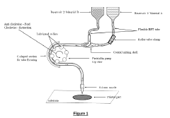
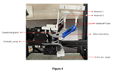
- A system utilizing a continuous feed mechanism with a peristaltic pump and a specialized coaxial casing for mixing inks from separate supplies, allowing for controlled ink propulsion and in-process composition modulation, enabling precise deposition of composite inks for intricate 3D structures.
Composite photocatalytic material for 3D printing and preparation method thereof
PatentInactiveCN117696126A
Innovation
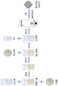
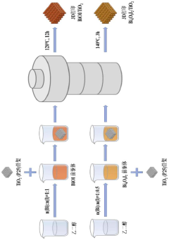
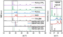
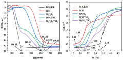
- Composite photocatalytic materials are prepared using 3D printing technology. The TiO2 precursor solution is formed by mixing citric acid, absolute ethanol, tetrabutyl titanate and titanium dioxide P25 powder, and mixed with bismuth nitrate pentahydrate, potassium iodide and ethylene glycol. The BixOyIz precursor solution undergoes a solvothermal reaction to form a BixOyIz/TiO2 composite material, which improves the photocatalytic performance and recovery rate of the material.
Environmental Impact and Sustainability Considerations
The environmental impact of Direct Ink Writing (DIW) technologies for flexible electronics using conductive ceramic-polymer inks presents both challenges and opportunities for sustainable development. The manufacturing process of these specialized inks typically involves energy-intensive production methods and potentially hazardous materials, raising concerns about their ecological footprint. Particularly, the synthesis of ceramic nanoparticles often requires high-temperature processing, contributing to significant energy consumption and associated carbon emissions.
The disposal and end-of-life management of flexible electronic devices manufactured with ceramic-polymer inks pose additional environmental challenges. Unlike traditional electronics, these hybrid materials may not fit neatly into existing recycling streams, potentially leading to increased electronic waste. The composite nature of these materials—combining ceramics, polymers, and conductive elements—complicates separation processes necessary for effective recycling.
However, recent advancements in green chemistry approaches are creating more sustainable pathways for conductive ink formulation. Water-based ceramic-polymer ink systems are emerging as environmentally preferable alternatives to solvent-based formulations, reducing volatile organic compound (VOC) emissions during manufacturing and application processes. Additionally, research into biodegradable polymer matrices compatible with ceramic fillers shows promise for developing more environmentally benign electronic components.
The extended lifespan of flexible electronics produced via DIW techniques may offset some environmental concerns through reduced replacement frequency. These devices typically demonstrate superior mechanical durability compared to conventional rigid electronics, potentially decreasing the overall material throughput in consumer electronic sectors. Furthermore, the additive nature of DIW manufacturing inherently minimizes material waste compared to subtractive manufacturing methods, aligning with principles of resource efficiency.
Energy efficiency improvements in DIW processing equipment are also contributing to reduced environmental impact. Low-temperature curing systems and energy-efficient sintering technologies are decreasing the carbon footprint associated with post-deposition processing of ceramic-polymer inks. These technological innovations, coupled with increasing industry adoption of renewable energy sources for manufacturing facilities, represent significant steps toward more sustainable production practices.
Regulatory frameworks worldwide are increasingly addressing the environmental aspects of advanced manufacturing technologies, including DIW for flexible electronics. Extended Producer Responsibility (EPR) policies are encouraging manufacturers to consider full lifecycle impacts of their products, while restrictions on hazardous substances are driving innovation in non-toxic ink formulations. These regulatory pressures, combined with growing consumer demand for sustainable electronics, are accelerating industry transition toward greener manufacturing approaches and materials.
Manufacturing Scalability and Process Integration
The scalability of Direct Ink Writing (DIW) for conductive ceramic-polymer inks presents both significant opportunities and challenges for flexible electronics manufacturing. Current production capabilities demonstrate promising throughput rates, with advanced DIW systems capable of processing multiple devices simultaneously through multi-nozzle configurations. These systems have achieved production speeds of up to 300 mm/s while maintaining resolution integrity, representing a substantial improvement over earlier generations of printing technology.
Integration of DIW processes into existing manufacturing lines requires careful consideration of compatibility factors. The relatively low curing temperatures of ceramic-polymer composite inks (typically 120-200°C) provide an advantage over traditional metal-based conductors that require sintering at temperatures exceeding 800°C. This temperature compatibility enables integration with temperature-sensitive polymer substrates common in flexible electronics applications.
Process standardization remains a critical challenge for widespread industrial adoption. The rheological properties of conductive ceramic-polymer inks must be precisely controlled to ensure consistent extrusion behavior across different production batches and environmental conditions. Recent advancements in real-time viscosity monitoring and feedback systems have improved process reliability, with reported consistency variations reduced to below 5% in controlled manufacturing environments.
Equipment scaling considerations include the transition from laboratory-scale printers to industrial production systems. Key developments include automated substrate handling, in-line quality control systems, and continuous ink supply mechanisms that eliminate production interruptions. Industry leaders have demonstrated pilot production lines capable of processing flexible electronic components at rates exceeding 10,000 units per day, suggesting viable pathways to mass production.
Post-processing integration presents another critical aspect of manufacturing scalability. The development of rapid curing technologies, including UV-assisted thermal curing and specialized IR systems, has reduced post-print processing times from hours to minutes. These advancements significantly improve production throughput while maintaining the electrical performance characteristics of the printed conductive features.
Cost analysis of scaled DIW manufacturing indicates potential economic advantages compared to traditional electronics fabrication methods. Material utilization efficiency exceeds 90% in optimized systems, substantially reducing waste compared to subtractive manufacturing approaches. Additionally, the reduced capital equipment requirements and facility specifications make DIW particularly suitable for distributed manufacturing models that can adapt quickly to market demands.
Unlock deeper insights with Patsnap Eureka Quick Research — get a full tech report to explore trends and direct your research. Try now!
Generate Your Research Report Instantly with AI Agent
Supercharge your innovation with Patsnap Eureka AI Agent Platform!