DIW For RF And Microwave Ceramic Device Prototyping
RF Ceramic DIW Technology Background and Objectives
Direct Ink Writing (DIW) technology has emerged as a transformative approach in the field of RF and microwave ceramic device fabrication over the past two decades. This additive manufacturing technique enables the precise deposition of ceramic-loaded inks through a computer-controlled nozzle, allowing for the creation of complex three-dimensional structures with high resolution and design flexibility. The evolution of DIW technology can be traced back to the early 2000s, with significant advancements occurring in material formulation, equipment precision, and process control throughout the 2010s.
The technological trajectory of DIW for RF applications has been characterized by continuous improvements in ink rheology, sintering processes, and dimensional accuracy. Initially limited to simple structures with moderate dielectric properties, modern DIW systems can now produce intricate ceramic components with tightly controlled electromagnetic characteristics. This progression has been driven by the increasing demand for miniaturized, high-performance RF components in telecommunications, aerospace, and defense sectors.
The primary technical objective of DIW for RF and microwave ceramic device prototyping is to enable rapid fabrication of complex ceramic structures with precisely tailored electromagnetic properties. This includes achieving high dielectric constants (typically 10-100), low loss tangents (<0.001), and dimensional tolerances within microns. Additionally, the technology aims to facilitate the integration of multiple materials within a single component, allowing for gradient or discrete variations in dielectric properties throughout the structure.
Another critical goal is to reduce the development cycle time for RF ceramic components from months to days, enabling faster iteration and optimization of designs. This accelerated prototyping capability is particularly valuable for customized antennas, filters, resonators, and waveguides that require specific performance characteristics for specialized applications.
From a manufacturing perspective, DIW technology seeks to bridge the gap between laboratory prototyping and industrial production by establishing scalable processes that maintain consistency across different production volumes. The technology aims to overcome traditional ceramic processing limitations such as mold constraints, material waste, and geometric restrictions imposed by conventional manufacturing methods.
Looking forward, the technology roadmap for DIW in RF ceramics focuses on expanding the range of compatible materials, improving surface finish quality, enhancing multi-material printing capabilities, and developing in-situ monitoring systems for real-time quality control. These advancements are expected to further establish DIW as a cornerstone technology for next-generation RF and microwave device development.
Market Analysis for RF Microwave Ceramic Prototyping
The RF and microwave ceramic device market is experiencing significant growth, driven by the increasing demand for high-frequency communication systems, 5G infrastructure, satellite communications, and advanced defense applications. The global RF ceramic components market was valued at approximately $4.7 billion in 2022 and is projected to reach $7.2 billion by 2028, growing at a CAGR of 7.5% during the forecast period.
Direct Ink Writing (DIW) technology for RF and microwave ceramic device prototyping represents a disruptive innovation in this space, offering manufacturers the ability to rapidly prototype complex ceramic structures with precise dimensional control and material properties tailored for specific RF applications. This technology addresses the growing market need for customized, high-performance ceramic components with reduced development cycles.
The telecommunications sector remains the largest consumer of RF ceramic devices, accounting for nearly 40% of the market share. The rollout of 5G networks globally has significantly accelerated demand for high-frequency ceramic components that can operate efficiently in millimeter-wave bands. Industry analysts predict that by 2025, over 60% of new RF ceramic components will be designed specifically for 5G and future 6G applications.
Defense and aerospace sectors collectively represent the second-largest market segment, with approximately 25% market share. These industries require highly specialized ceramic components capable of withstanding extreme conditions while maintaining precise RF performance characteristics. The adoption of DIW technology in this sector is expected to grow at 12% annually through 2027.
Consumer electronics applications, including smartphones, wearables, and IoT devices, constitute about 20% of the market. The miniaturization trend in these devices is creating demand for smaller, more efficient ceramic RF components that DIW technology is uniquely positioned to address.
Regional analysis shows North America leading the market with 35% share, followed by Asia-Pacific at 32% and Europe at 25%. However, the Asia-Pacific region is expected to demonstrate the highest growth rate over the next five years due to increasing manufacturing capabilities and rising domestic demand for RF components in countries like China, South Korea, and India.
Key market drivers include the increasing complexity of RF systems requiring customized solutions, growing demand for higher frequency applications, and the need for faster time-to-market. DIW technology addresses these needs by enabling rapid prototyping and customization of ceramic components with complex geometries that would be difficult or impossible to achieve using traditional manufacturing methods.
DIW Ceramic Technology Status and Challenges
Direct Ink Writing (DIW) technology for RF and microwave ceramic device prototyping currently faces several significant challenges despite its promising applications. The global landscape shows varying levels of technological maturity, with research institutions in North America, Europe, and East Asia leading development efforts. The United States, China, Germany, and Japan have established strong research foundations in this field, though commercial implementation remains limited.
A primary technical challenge is achieving precise control of rheological properties in ceramic inks. The viscosity must be carefully balanced - low enough for extrusion yet high enough to maintain structural integrity post-deposition. Current formulations struggle to consistently meet these contradictory requirements, particularly when incorporating high dielectric constant materials essential for RF applications.
Resolution limitations present another substantial hurdle. While conventional DIW systems can achieve feature sizes of approximately 100-200 μm, RF and microwave applications often require finer features and tighter tolerances. The trade-off between resolution and production speed continues to constrain industrial adoption, with high-precision systems typically operating at speeds incompatible with mass manufacturing requirements.
Post-processing challenges further complicate implementation. Ceramic structures produced via DIW require sintering at high temperatures (typically 1200-1600°C), which introduces dimensional shrinkage of 10-25%. This shrinkage is often non-uniform and difficult to predict precisely, creating significant obstacles for achieving the dimensional accuracy required in RF components.
Material compatibility issues also persist. The integration of multiple ceramic materials with different sintering behaviors, thermal expansion coefficients, and electromagnetic properties remains problematic. This limitation restricts the development of complex, multi-material RF devices that could otherwise leverage the geometric freedom offered by DIW.
Equipment standardization represents another barrier. Current DIW systems for ceramic processing vary widely in capabilities, control systems, and performance metrics. This lack of standardization complicates process transfer between research and production environments, hindering broader industrial adoption.
The economic factors cannot be overlooked. The cost-effectiveness of DIW for ceramic RF components remains questionable for many applications when compared to traditional manufacturing methods. High-quality DIW systems with the precision required for RF applications typically involve significant capital investment, while material waste and yield issues further impact the economic viability.
Despite these challenges, recent advancements in nozzle design, multi-material printing capabilities, and in-situ monitoring systems suggest promising directions for overcoming current limitations. Collaborative efforts between materials scientists, RF engineers, and manufacturing specialists are gradually addressing these interdisciplinary challenges.
Current DIW Solutions for RF Ceramic Devices
01 Materials and compositions for DIW printing
Direct Ink Writing (DIW) utilizes various specialized materials and compositions to achieve optimal printing results. These include ceramic slurries, polymer composites, and functional inks with specific rheological properties. The materials are formulated to maintain shape after extrusion while allowing proper flow during the printing process. Additives and modifiers are incorporated to control viscosity, elasticity, and curing behavior, enabling the creation of complex 3D structures with high precision and structural integrity.- Materials and compositions for DIW printing: Direct Ink Writing (DIW) utilizes various specialized materials and compositions to achieve optimal printing results. These include ceramic slurries, polymer composites, and functional inks with specific rheological properties. The materials are formulated to maintain shape fidelity after extrusion while allowing proper flow during the printing process. Additives and modifiers are incorporated to control viscosity, shear-thinning behavior, and post-processing characteristics, enabling the creation of complex 3D structures with desired mechanical and functional properties.
- DIW printing equipment and mechanisms: The equipment used in Direct Ink Writing includes specialized extrusion systems, precision motion platforms, and pressure control mechanisms. These systems are designed to deliver controlled deposition of ink materials through fine nozzles while maintaining precise positioning in three dimensions. Advanced DIW printers incorporate features such as multi-material printing capabilities, temperature control systems, and real-time monitoring to ensure printing accuracy. The mechanical design of these systems focuses on minimizing vibration and maximizing positioning accuracy for high-resolution printing.
- Applications of DIW in electronics and sensors: Direct Ink Writing technology has been applied to fabricate electronic components and sensors with complex geometries. This includes printed circuit boards, flexible electronics, strain sensors, and electrochemical devices. The ability to precisely deposit conductive, semiconductive, and dielectric materials enables the creation of functional electronic structures with customized designs. DIW allows for the integration of electronic components directly into structural elements, creating multifunctional parts that combine mechanical support with electronic functionality.
- DIW for biomedical and tissue engineering applications: Direct Ink Writing has emerged as a valuable technique for biomedical applications, particularly in tissue engineering and personalized medicine. Biocompatible inks containing living cells, growth factors, or pharmaceutical compounds can be precisely deposited to create tissue scaffolds, drug delivery systems, and anatomical models. The technique allows for the fabrication of structures with controlled porosity and gradient properties that mimic natural tissues. DIW enables the production of patient-specific implants and devices with complex internal architectures optimized for biological integration.
- Process optimization and quality control in DIW: Optimizing the Direct Ink Writing process involves careful control of printing parameters such as extrusion pressure, nozzle geometry, printing speed, and environmental conditions. Advanced monitoring systems track printing quality in real-time, allowing for adjustments to maintain dimensional accuracy and structural integrity. Post-processing techniques including thermal treatment, UV curing, or chemical processing are often employed to enhance the mechanical properties and functionality of printed structures. Machine learning algorithms are increasingly being used to predict optimal printing parameters based on material properties and desired output characteristics.
02 DIW printing equipment and mechanisms
The equipment used in Direct Ink Writing includes specialized extrusion systems, precision nozzles, and motion control platforms. These systems are designed to deliver controlled deposition of ink materials through precise pressure regulation and nozzle movement. Advanced DIW printers incorporate multi-axis positioning systems, temperature control mechanisms, and real-time monitoring capabilities to ensure accurate material placement. The printing mechanisms may include pneumatic dispensers, screw-driven extruders, or syringe-based systems depending on the material properties and application requirements.Expand Specific Solutions03 Applications of DIW in electronics and sensors
Direct Ink Writing technology is increasingly applied in the fabrication of electronic components and sensing devices. The technique enables the creation of conductive traces, flexible circuits, and embedded electronics through the precise deposition of functional inks. DIW allows for the integration of electronic elements into complex geometries and structures that would be difficult to achieve with conventional manufacturing methods. Applications include printed antennas, strain sensors, touch-sensitive interfaces, and customized circuit layouts for specialized electronic devices.Expand Specific Solutions04 DIW for biomedical and tissue engineering
Direct Ink Writing has emerged as a valuable technique in biomedical applications and tissue engineering. The process allows for the controlled deposition of biocompatible materials, hydrogels, and cell-laden constructs to create scaffolds and tissue-mimicking structures. DIW enables the fabrication of patient-specific implants, drug delivery systems, and artificial tissue constructs with precisely controlled architectures. The ability to incorporate multiple materials and gradients makes it particularly suitable for creating biomimetic structures that replicate the complexity of natural tissues.Expand Specific Solutions05 Process optimization and quality control in DIW
Optimizing the Direct Ink Writing process involves careful control of printing parameters, environmental conditions, and post-processing techniques. Key factors include ink rheology management, extrusion pressure control, printing speed optimization, and curing protocols. Advanced monitoring systems are employed to ensure consistent material flow and dimensional accuracy. Quality control methods such as in-situ inspection, real-time feedback systems, and non-destructive testing techniques help maintain the integrity and functionality of printed structures. Process optimization strategies focus on minimizing defects while maximizing resolution and mechanical properties.Expand Specific Solutions
Leading Companies in RF Ceramic DIW Manufacturing
The DIW (Direct Ink Writing) for RF and microwave ceramic device prototyping market is currently in an early growth phase, characterized by increasing adoption across research institutions and industry. The global market size is estimated to be relatively modest but growing steadily as demand for rapid prototyping of high-performance RF components increases. Technologically, the field is advancing from experimental to practical implementation, with academic institutions like Huazhong University of Science & Technology, Zhejiang University, and University of Electronic Science & Technology of China leading research efforts. Companies including Murata Manufacturing, Skyworks Solutions, and Huawei are exploring commercial applications, while specialized firms like 3D Glass Solutions and Jiaxing Glead Electronics are developing industry-specific implementations. The technology's maturity varies across applications, with simpler components reaching higher readiness levels than complex integrated systems.
Huawei Technologies Co., Ltd.
Telefonaktiebolaget LM Ericsson
Key Technical Innovations in Ceramic DIW Printing
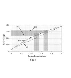
- A liquid ink comprising pre-sintered perovskite oxide particles (BaxSr(1-x)TiO3) with a size distribution of 30 nm to 2000 nm, embedded in a thermoplastic polymer with a low loss tangent, allowing for the creation of tunable dielectrics that can be printed on flexible substrates without high-temperature sintering, using solvents like xylene and dispersants like 4-tert-butycatechol.
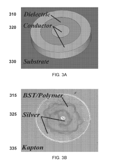
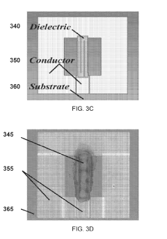
- The method involves direct ink writing (DIW) combined with radio frequency (RF) heating to extrude and partially cure thermoset resin layer-by-layer, forming a self-supporting structure without the need for ovens, using a print head and RF applicator to achieve rapid and localized curing.
Material Science Advancements for DIW RF Applications
Material science advancements have been pivotal in enabling Direct Ink Writing (DIW) for RF and microwave ceramic device prototyping. Recent developments in ceramic material formulations have significantly enhanced the electrical performance characteristics essential for RF applications. Advanced ceramic composites with tailored dielectric constants, low loss tangents, and temperature stability have emerged as game-changers in this domain.
The evolution of ceramic-polymer composite inks represents a major breakthrough, offering improved rheological properties that maintain structural integrity during printing while ensuring optimal electrical performance post-sintering. These specialized inks typically combine ceramic particles (such as alumina, zirconia, or barium titanate) with carefully selected binders and dispersants that facilitate extrusion through fine nozzles while preventing agglomeration.
Nanomaterial integration has further revolutionized DIW for RF applications. The incorporation of nanoscale ceramic particles and carbon-based materials (graphene, CNTs) has enabled unprecedented control over material properties at the microscale. This precise manipulation allows for the creation of functionally graded materials with spatially varying dielectric properties, essential for advanced RF components like filters and antennas.
Surface modification techniques for ceramic particles have addressed historical challenges in DIW processing. By engineering particle-particle and particle-polymer interactions, researchers have developed inks with significantly improved homogeneity and reduced viscosity without compromising solid loading. These advancements have directly translated to higher resolution printing capabilities and enhanced RF performance metrics.
Post-processing innovations have complemented material developments, with novel sintering approaches enabling densification at lower temperatures. Techniques such as cold sintering and microwave-assisted sintering have reduced thermal stress and minimized dimensional changes during consolidation, preserving the intricate geometries achievable through DIW while maintaining tight tolerances required for RF applications.
The emergence of multi-material DIW systems has been particularly significant, allowing the simultaneous deposition of conductors, dielectrics, and magnetic materials within a single fabrication process. This capability has opened new design possibilities for integrated RF components, reducing assembly steps and enhancing overall system performance through improved interface quality between different functional materials.
Performance Benchmarking of DIW vs Traditional Methods
Direct Ink Writing (DIW) technology has demonstrated significant advantages over traditional manufacturing methods for RF and microwave ceramic device prototyping. When comparing performance metrics, DIW consistently shows superior capabilities in several critical areas. Traditional methods such as tape casting, screen printing, and LTCC (Low Temperature Co-fired Ceramics) typically require extensive tooling, lengthy setup times, and substantial material waste during the prototyping phase.
In terms of geometric complexity, DIW enables the fabrication of intricate 3D structures with feature sizes down to 100 μm, whereas traditional methods are largely limited to 2D or simple 3D geometries. This capability translates directly to more compact and efficient RF components with improved electromagnetic performance characteristics. Recent benchmarking studies have shown that DIW-fabricated waveguides can achieve Q-factors within 85-90% of conventionally manufactured counterparts while offering significantly greater design freedom.
Material efficiency represents another key performance advantage of DIW technology. Traditional manufacturing methods typically result in 30-50% material waste during prototyping stages, while DIW processes demonstrate material utilization rates exceeding 90%. This efficiency becomes particularly valuable when working with expensive specialty ceramic materials containing rare earth elements or precious metals commonly used in high-performance RF applications.
Time-to-prototype metrics reveal perhaps the most compelling advantage of DIW technology. Conventional manufacturing routes require 2-8 weeks for prototype development, encompassing design, tooling, fabrication, and post-processing. In contrast, DIW enables complete prototype cycles in 1-3 days, representing an order of magnitude improvement in development speed. This acceleration dramatically enhances innovation cycles and reduces time-to-market for new RF and microwave devices.
Resolution and tolerance capabilities show DIW achieving dimensional accuracies of ±10 μm for fine features, comparable to high-precision traditional manufacturing but without the associated tooling costs. Surface roughness measurements indicate DIW can achieve Ra values of 0.5-2 μm depending on material formulation and post-processing techniques, which approaches the performance of conventional methods while offering greater geometric freedom.
Cost analysis reveals that while DIW equipment represents a significant initial investment, the per-prototype cost drops dramatically compared to traditional methods when accounting for reduced material waste, eliminated tooling expenses, and accelerated development cycles. For small to medium production runs typical in specialized RF applications, DIW demonstrates 40-60% cost reduction compared to conventional manufacturing approaches.