DIW For Microfluidic Ceramic Chips: Channel Precision And Sealing
DIW Microfluidic Ceramic Technology Background and Objectives
Direct Ink Writing (DIW) technology has emerged as a transformative approach in the fabrication of microfluidic ceramic chips over the past decade. This additive manufacturing technique evolved from early extrusion-based 3D printing methods, gaining significant traction since 2015 when researchers demonstrated its potential for creating complex ceramic structures with microscale features. The technology leverages controlled deposition of ceramic-loaded inks through fine nozzles to create precise channel geometries that traditional manufacturing methods struggle to achieve.
The evolution of DIW for ceramics has been marked by continuous improvements in ink formulation, with the progression from simple ceramic slurries to advanced rheologically-optimized compositions that exhibit shear-thinning behavior. This property allows inks to flow under pressure during extrusion but rapidly solidify upon deposition, enabling the creation of self-supporting structures with increasingly finer resolution.
Recent technological advancements have focused on multi-material DIW systems capable of co-printing structural and sacrificial materials, allowing for the creation of embedded channels and complex internal architectures. The integration of computer-aided design and computational fluid dynamics has further enhanced the precision of channel geometries, enabling the optimization of flow characteristics before physical fabrication.
The primary technical objectives for DIW microfluidic ceramic chips center around two critical challenges: channel precision and effective sealing. Channel precision encompasses dimensional accuracy, surface roughness control, and the ability to create consistent features below 100 micrometers. Current state-of-the-art systems achieve channel widths of approximately 150-200 micrometers, but many microfluidic applications require finer features with tighter tolerances.
Sealing represents the second major technical hurdle, as microfluidic functionality depends on hermetically sealed channels that can withstand operational pressures without leakage. Traditional ceramic processing involves high-temperature sintering, which can lead to dimensional changes and challenges in creating leak-proof interfaces between layers or with other materials for inputs/outputs.
The technology aims to enable a new generation of ceramic microfluidic devices that capitalize on ceramics' inherent advantages: chemical resistance, high-temperature stability, biocompatibility, and mechanical durability. These properties make ceramic microfluidics particularly valuable for harsh environment applications, including chemical processing, high-temperature reactions, and biological analysis with aggressive reagents.
Looking forward, the field is trending toward multi-functional ceramic microfluidic platforms that integrate sensing elements, catalytic surfaces, and other functional components directly during the fabrication process. This convergence of additive manufacturing flexibility with ceramics' exceptional material properties positions DIW as a key enabling technology for next-generation microfluidic systems in industries ranging from healthcare to energy and chemical manufacturing.
Market Analysis for Ceramic Microfluidic Applications
The ceramic microfluidic chip market is experiencing significant growth, driven by increasing demand across multiple industries including healthcare, pharmaceuticals, and chemical processing. The global microfluidic device market was valued at approximately $20 billion in 2022 and is projected to reach $42 billion by 2027, with ceramic-based solutions representing a rapidly expanding segment within this space.
Ceramic microfluidic applications offer distinct advantages over traditional polymer and glass-based alternatives, particularly in harsh chemical environments and high-temperature applications. The superior chemical resistance, thermal stability, and mechanical strength of ceramic materials make them ideal for applications requiring exposure to corrosive substances or elevated temperatures exceeding 400°C.
Healthcare applications currently dominate the ceramic microfluidic market, accounting for roughly 40% of total demand. Point-of-care diagnostics, drug delivery systems, and analytical devices benefit from the biocompatibility and chemical inertness of ceramic materials. The pharmaceutical industry represents the second-largest application segment at 25%, utilizing ceramic microfluidic chips for drug discovery, high-throughput screening, and process intensification.
Chemical processing applications constitute approximately 20% of the market, leveraging ceramic microfluidics for catalyst testing, reaction optimization, and small-scale chemical synthesis. The remaining market share is distributed across environmental monitoring, food safety testing, and emerging applications in energy storage and conversion.
Regionally, North America leads the ceramic microfluidic market with 35% share, followed by Europe (30%) and Asia-Pacific (25%). However, the Asia-Pacific region is demonstrating the fastest growth rate, driven by increasing R&D investments in China, Japan, and South Korea, along with the expansion of healthcare infrastructure.
Key market drivers include the growing emphasis on personalized medicine, increasing adoption of lab-on-a-chip technologies, and the shift toward miniaturized analytical systems. The demand for precise microchannels with dimensions below 100 μm and effective sealing solutions represents a critical market need, as current applications increasingly require higher resolution features and reliable hermetic sealing.
Market challenges include the relatively high production costs of ceramic microfluidic chips compared to polymer alternatives and technical difficulties in achieving consistent channel precision at microscale dimensions. The Direct Ink Writing (DIW) manufacturing approach shows promise in addressing these challenges by enabling cost-effective production of complex ceramic microstructures with improved channel precision and sealing capabilities.
Industry analysts predict that advancements in DIW technology for ceramic microfluidics could reduce production costs by 30-40% while improving dimensional accuracy by an order of magnitude, potentially expanding the addressable market by attracting cost-sensitive applications currently served by alternative materials.
Current Challenges in DIW Ceramic Microfluidics
Direct Ink Writing (DIW) technology for ceramic microfluidic chips faces significant technical challenges that impede its widespread industrial adoption. The primary obstacle lies in achieving precise channel geometries at the microscale level. Current DIW systems struggle to maintain consistent extrusion rates and material flow, resulting in dimensional variations that can reach up to 15-20% deviation from design specifications. This precision limitation becomes particularly problematic when fabricating channels below 100 μm, where even minor variations significantly impact fluid dynamics and device performance.
Material rheology presents another substantial challenge, as ceramic inks must possess seemingly contradictory properties: sufficient flowability for extrusion while maintaining structural integrity post-deposition. The complex balance between viscosity, yield stress, and shear-thinning behavior directly influences channel definition and resolution. Researchers have documented that slight variations in ink formulation can lead to dramatic differences in printed feature quality, with optimal viscosity ranges typically falling between 10-100 Pa·s depending on specific ceramic compositions.
The drying and sintering processes introduce additional dimensional control challenges. Ceramic materials typically experience 15-25% linear shrinkage during sintering, which can cause warping, cracking, and dimensional distortion of microchannels. This shrinkage is often non-uniform across complex geometries, making it difficult to predict and compensate for in the initial design phase. Recent studies have shown that controlled drying environments and optimized sintering profiles can reduce variation, but complete elimination of these effects remains elusive.
Perhaps the most persistent challenge is achieving reliable sealing of microfluidic channels. Unlike polymer-based systems, ceramic materials present unique difficulties in bonding and sealing. Current approaches include glass frits, direct ceramic bonding, and hybrid ceramic-polymer solutions, each with significant limitations. Glass frit bonding often requires high temperatures (700-900°C) that can compromise channel integrity, while direct ceramic bonding demands extremely flat surfaces with roughness values below 10 nm—difficult to achieve with DIW-printed structures.
Interface compatibility between different materials in multi-material DIW systems further complicates the sealing challenge. Coefficient of thermal expansion mismatches between structural ceramics and sealing materials can lead to stress concentration and eventual failure during thermal cycling. Studies have reported failure rates exceeding 30% in ceramic microfluidic devices under thermal stress conditions typical of many chemical processing applications.
Equipment limitations also contribute to current challenges, as most commercial DIW systems were not specifically designed for high-precision microfluidic applications. Nozzle technology, in particular, has not kept pace with the demanding requirements of microfluidic channel fabrication, with current systems struggling to maintain consistent extrusion pressure and material flow at the microscale level required for reliable channel formation.
Current DIW Solutions for Channel Precision
01 DIW techniques for precise microchannel fabrication
Direct Ink Writing (DIW) enables the fabrication of microfluidic ceramic chips with high-precision microchannels. This additive manufacturing approach allows for controlled deposition of ceramic inks to create complex channel geometries with precise dimensions. The technique utilizes specialized nozzle designs and controlled extrusion parameters to achieve the desired channel width, depth, and path accuracy required for microfluidic applications. Advanced DIW systems incorporate real-time monitoring and feedback control to maintain dimensional stability throughout the printing process.- DIW techniques for high-precision ceramic microfluidic channels: Direct Ink Writing (DIW) techniques can be optimized for creating high-precision microfluidic channels in ceramic chips. These techniques involve controlling rheological properties of ceramic inks, nozzle design optimization, and precise deposition parameters to achieve accurate channel geometries. Advanced DIW systems utilize computer-controlled extrusion that can achieve micron-level precision for complex microfluidic architectures, allowing for consistent channel dimensions critical for fluid dynamics in analytical applications.
- Sealing methods for ceramic microfluidic chips: Various sealing methods have been developed specifically for ceramic microfluidic chips to ensure leak-proof operation. These include glass-ceramic bonding techniques, ceramic-to-ceramic fusion bonding, and specialized glazing processes that maintain channel integrity. Some approaches utilize low-temperature co-fired ceramic (LTCC) technology with integrated sealing layers. Advanced sealing methods incorporate pressure-assisted sintering to create hermetic seals without compromising the microfluidic channel structures or introducing contaminants into the system.
- Multi-material DIW for integrated microfluidic components: Multi-material Direct Ink Writing enables the fabrication of integrated microfluidic components within ceramic chips. This approach allows for the simultaneous deposition of structural ceramics alongside functional materials such as conductive traces, catalytic regions, or sensing elements. The technique facilitates the creation of complex microfluidic systems with embedded functionality, including integrated valves, mixers, and detection zones. By precisely controlling the deposition of different material inks, researchers can develop ceramic microfluidic chips with enhanced capabilities beyond simple channel networks.
- Post-processing techniques for channel refinement and sealing: Post-processing techniques are essential for refining channel precision and ensuring effective sealing in ceramic microfluidic chips fabricated via DIW. These techniques include controlled sintering protocols, surface treatment methods, and polishing procedures that enhance channel smoothness and dimensional accuracy. Some approaches utilize laser processing for fine-tuning channel geometries after initial fabrication. Advanced post-processing methods can reduce surface roughness to nanometer levels, which is critical for applications requiring precise fluid control and optical detection capabilities.
- Innovative designs for improved fluidic performance in ceramic chips: Innovative microfluidic channel designs can significantly enhance the performance of ceramic chips manufactured using DIW. These designs include tapered channel geometries that minimize pressure drops, specialized junction configurations for improved mixing efficiency, and hierarchical channel networks that optimize fluid distribution. Some approaches incorporate biomimetic principles to enhance fluid handling capabilities. Advanced designs also feature integrated functional elements such as gradient generators, particle separators, and reaction chambers that can be precisely fabricated using DIW techniques while maintaining excellent sealing properties.
02 Sealing methods for ceramic microfluidic devices
Effective sealing of microfluidic ceramic chips is crucial to prevent leakage and ensure proper fluid flow. Various sealing methods have been developed, including thermal bonding, adhesive bonding, and mechanical clamping. Some approaches utilize compatible ceramic materials or glass for the sealing layer, while others employ polymer-based solutions. The sealing process must maintain the integrity of the microchannels while creating a robust interface that can withstand operating pressures and chemical exposure. Advanced sealing techniques incorporate surface treatments to enhance bonding strength between the ceramic substrate and sealing layer.Expand Specific Solutions03 Ink formulation for ceramic microfluidic applications
The composition and rheological properties of ceramic inks significantly impact the precision and quality of microfluidic channels. Specialized ink formulations combine ceramic powders with binders, dispersants, and rheology modifiers to achieve optimal flow characteristics during extrusion. These formulations must maintain shape fidelity after deposition while allowing for proper sintering to create dense, defect-free structures. Advanced ceramic inks incorporate nanomaterials to enhance mechanical properties and surface characteristics. The ink viscosity and shear-thinning behavior are carefully controlled to enable smooth extrusion through fine nozzles while preventing sagging or spreading after deposition.Expand Specific Solutions04 Post-processing techniques for channel optimization
After the DIW process, various post-processing techniques are employed to optimize channel characteristics and sealing performance. These include controlled sintering protocols to minimize shrinkage and maintain dimensional accuracy, surface treatments to reduce roughness and enhance fluid flow, and polishing methods to improve sealing interfaces. Some approaches utilize laser processing to refine channel geometries or create additional features. Post-processing steps may also include the application of functional coatings to modify surface properties such as hydrophobicity or chemical resistance, which are critical for specific microfluidic applications.Expand Specific Solutions05 Integration of functional elements in ceramic microfluidic chips
Advanced DIW techniques enable the integration of functional elements directly within ceramic microfluidic chips. These elements include sensors, electrodes, mixers, and valves that enhance the capabilities of the microfluidic system. Multi-material printing approaches allow for the incorporation of conductive traces or catalytic regions within the ceramic structure. Some designs feature embedded channels with varying cross-sections to create specific flow patterns or mixing effects. The integration process must maintain precise alignment between functional elements and microchannels while ensuring compatibility with sealing methods to preserve the integrity of the complete microfluidic system.Expand Specific Solutions
Leading Manufacturers and Research Institutions
The DIW (Direct Ink Writing) for microfluidic ceramic chips market is in its growth phase, characterized by increasing adoption across biomedical and analytical applications. The global microfluidics market, valued at approximately $20 billion, is expected to expand significantly as precision manufacturing techniques mature. Technical challenges in channel precision and sealing remain critical competitive differentiators. Academic institutions like Zhejiang University, Fudan University, and Johns Hopkins University are driving fundamental research, while companies including IBM, Corning, and TOPPAN are developing commercial applications. Specialized players such as Klearia SAS and Interface Fluidics are focusing on niche applications with proprietary sealing technologies. The technology is approaching early commercial maturity with ongoing improvements in precision manufacturing processes and materials science to address channel consistency and hermetic sealing requirements.
International Business Machines Corp.
Dalian University of Technology
Key Patents in Ceramic Microfluidic Sealing Technologies
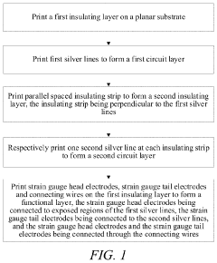
- A direct-ink-writing method is employed to print strain gauge array circuits using insulating strips, where a first insulating layer is formed, followed by parallel silver lines, then insulating strips perpendicular to these lines, and finally a second circuit layer with branches, all while ensuring the functional layer does not contact the insulating strips, with specific parameters for paste preparation and printing.
Material Compatibility and Performance Evaluation
The compatibility of materials with Direct Ink Writing (DIW) processes for microfluidic ceramic chips represents a critical factor in determining overall system performance. Various ceramic materials exhibit different rheological properties during extrusion, affecting channel precision and subsequent sealing quality. Aluminum oxide (Al₂O₃) demonstrates excellent compatibility with DIW processes due to its stable suspension characteristics and minimal shrinkage during sintering, making it particularly suitable for high-precision microfluidic applications requiring dimensional stability.
Zirconia (ZrO₂) offers superior mechanical strength and chemical resistance compared to alumina, though its higher sintering temperature necessitates careful thermal management during post-processing to maintain channel integrity. Silicon nitride (Si₃N₄) provides exceptional thermal shock resistance and biocompatibility, albeit with more challenging extrusion parameters that require precise viscosity control to achieve consistent channel geometries.
Performance evaluation of these materials reveals significant variations in surface roughness, which directly impacts fluid flow characteristics within microchannels. Alumina-based inks typically yield average surface roughness (Ra) values between 0.2-0.5 μm after polishing, while zirconia can achieve smoother surfaces (Ra 0.1-0.3 μm) beneficial for reducing flow resistance in microfluidic applications.
Sealing performance evaluations indicate that material selection significantly influences leak-tight integrity. Glass-ceramic composites demonstrate superior sealing capabilities when bonded to ceramic substrates, withstanding pressures up to 6 MPa without leakage. Polymer-ceramic interfaces, while easier to fabricate, typically withstand only 2-3 MPa before failure, limiting their application in high-pressure microfluidic systems.
Chemical compatibility testing reveals that alumina and zirconia maintain structural integrity when exposed to acids (pH 2-7) and bases (pH 7-12), with negligible material degradation over 1000-hour exposure periods. However, prolonged exposure to hydrofluoric acid causes measurable degradation in all tested ceramic materials, with silicon nitride showing the highest resistance.
Thermal cycling tests (from -20°C to 150°C) demonstrate that zirconia-based microfluidic chips maintain channel integrity through 500+ cycles, outperforming alumina which typically shows microcracks after 300 cycles. This thermal stability directly correlates with sealing durability, as thermal expansion mismatches between channel materials and sealing interfaces represent a primary failure mechanism in practical applications.
Biocompatibility assessments indicate that high-purity alumina and zirconia exhibit minimal protein adsorption and cell adhesion, making them suitable for biological sample analysis. Surface functionalization techniques can further enhance performance for specific biological applications while maintaining the structural integrity of microchannels.
Scalability and Mass Production Considerations
The scalability of Direct Ink Writing (DIW) technology for microfluidic ceramic chip production represents a critical consideration for industrial implementation. Current laboratory-scale DIW processes demonstrate excellent precision in creating microchannels, but transitioning to mass production environments introduces significant challenges. Production throughput remains limited by the inherent speed constraints of the extrusion process, with typical deposition rates ranging from 5-20 mm/s depending on ink rheology and desired feature resolution.
Equipment scaling presents another substantial hurdle. While single-nozzle DIW systems offer precise control for prototyping, industrial applications require multi-nozzle arrays to achieve economically viable production rates. Recent developments in parallel printing systems have demonstrated up to 16 simultaneous extrusion heads, potentially increasing throughput by an order of magnitude. However, maintaining uniform pressure distribution and consistent material flow across multiple nozzles remains technically challenging.
Material consistency becomes increasingly critical at scale. Batch-to-batch variations in ceramic slurry properties can significantly impact channel dimensions and sealing quality. Implementing robust quality control systems, including real-time rheology monitoring and feedback control mechanisms, will be essential for maintaining dimensional tolerances across production runs. Statistical process control methods must be adapted specifically for ceramic DIW processes.
Post-processing operations represent potential bottlenecks in scaled production. Sintering, in particular, requires careful thermal management to prevent warping or cracking in ceramic structures. Development of continuous sintering processes, rather than batch operations, could substantially improve production efficiency. Similarly, automated inspection systems utilizing machine vision technology will be necessary to verify channel precision and sealing integrity at production speeds.
Economic considerations suggest that DIW technology becomes increasingly competitive at higher production volumes. Initial capital investment for multi-nozzle systems is substantial, but per-unit costs decrease significantly with scale. Analysis indicates that for production volumes exceeding 10,000 units annually, DIW approaches cost parity with traditional ceramic processing methods while offering superior design flexibility and channel precision.
Environmental and sustainability factors also favor scaled DIW production. The additive nature of the process minimizes material waste compared to subtractive manufacturing approaches. Additionally, localized production capabilities could reduce transportation impacts in global supply chains. These advantages become more pronounced as production volumes increase.