

Evaluate Flexible Electronics Capacitive Coupling Effects
SEP 10, 202510 MIN READ
Generate Your Research Report Instantly with AI Agent
Patsnap Eureka helps you evaluate technical feasibility & market potential.
Flexible Electronics Capacitive Coupling Background and Objectives
Flexible electronics represents a revolutionary paradigm shift in electronic device design and manufacturing, enabling the creation of bendable, stretchable, and conformable electronic systems. The field has evolved significantly over the past two decades, transitioning from academic curiosity to commercial viability across multiple industries. Capacitive coupling effects in flexible electronics have emerged as both a challenge and an opportunity, influencing device performance, reliability, and functionality in ways fundamentally different from conventional rigid electronics.
The historical trajectory of flexible electronics began with the development of thin-film transistors on plastic substrates in the early 2000s, followed by significant advancements in materials science that enabled greater flexibility while maintaining electronic performance. Capacitive coupling, initially considered primarily as a parasitic effect, has gradually been recognized as a phenomenon that can be harnessed for novel sensing applications, energy harvesting, and signal transmission in flexible systems.
Current technological trends indicate an accelerating convergence of flexible form factors with advanced electronic functionalities, where capacitive coupling plays an increasingly central role. The field is moving toward ultra-thin, highly conformable electronics that can seamlessly integrate with curved surfaces, biological tissues, and dynamic environments where traditional rigid electronics cannot function effectively.
The primary objective of this technical evaluation is to comprehensively assess the fundamental mechanisms, measurement methodologies, and practical implications of capacitive coupling effects in flexible electronic systems. This includes quantifying how substrate deformation, bending radius, and mechanical stress alter capacitive coupling parameters compared to rigid counterparts.
Secondary objectives include identifying design strategies to either mitigate unwanted capacitive coupling or intentionally leverage these effects for enhanced functionality. This involves exploring novel materials, circuit topologies, and fabrication techniques specifically optimized for flexible electronic applications where capacitive coupling is a critical consideration.
Additionally, this evaluation aims to establish standardized testing protocols for characterizing capacitive coupling in flexible electronics across different operating conditions, including various degrees of mechanical deformation, environmental factors, and aging effects. Such standardization is essential for meaningful comparison between different technological approaches and for predicting long-term reliability.
The ultimate goal is to develop a comprehensive technical framework that enables engineers and researchers to accurately predict, model, and control capacitive coupling effects in next-generation flexible electronic devices, thereby accelerating innovation and commercial adoption across healthcare, consumer electronics, automotive, and industrial applications.
Market Demand Analysis for Flexible Electronic Devices
The flexible electronics market is experiencing unprecedented growth, driven by increasing consumer demand for wearable devices, foldable smartphones, and innovative healthcare monitoring systems. Current market projections indicate that the global flexible electronics sector will reach approximately $42 billion by 2027, with a compound annual growth rate exceeding 11% between 2022 and 2027. This robust growth trajectory underscores the significant market potential for technologies addressing capacitive coupling effects in flexible electronic systems.
Consumer electronics represents the largest application segment, with foldable displays and bendable smartphones leading adoption rates. Major manufacturers including Samsung, LG, and Huawei have already commercialized products incorporating flexible display technologies, signaling strong market acceptance. Industry surveys reveal that 67% of smartphone users express interest in devices with flexible form factors, highlighting substantial untapped market potential.
The healthcare and medical devices sector presents another high-growth opportunity area. Flexible biomedical sensors capable of continuous health monitoring are gaining traction, with market analysts predicting this segment will grow at nearly 15% annually through 2026. The ability to address capacitive coupling challenges in these applications directly correlates with device accuracy and reliability—critical factors for medical-grade equipment.
Industrial and automotive applications are emerging as significant market drivers as well. Flexible sensors and control systems that can conform to irregular surfaces are increasingly sought after for advanced manufacturing environments and next-generation vehicles. Market research indicates that industrial adoption of flexible electronics is expected to triple by 2025, with particular emphasis on solutions that maintain signal integrity despite mechanical deformation.
Regional market analysis reveals Asia-Pacific as the dominant manufacturing hub, accounting for approximately 58% of global production capacity. However, North America leads in research innovation and high-value applications, particularly in medical and aerospace sectors. European markets show strong demand for sustainable flexible electronic solutions with reduced environmental impact.
Customer pain points consistently highlight reliability concerns related to signal integrity when devices are bent or flexed—precisely the issues that capacitive coupling effect management addresses. Market surveys indicate that 72% of potential enterprise adopters cite signal stability during deformation as a critical purchasing consideration, while 64% of consumer users rank consistent performance during bending as "very important" or "essential."
The market landscape clearly demonstrates that solutions effectively addressing capacitive coupling effects in flexible electronics will command premium positioning, particularly in high-reliability applications where signal integrity is paramount. This represents a significant commercial opportunity for technologies that can overcome these technical challenges while maintaining manufacturing scalability.
Current State and Challenges in Capacitive Coupling Technology
Capacitive coupling technology in flexible electronics has witnessed significant advancements in recent years, yet continues to face substantial technical challenges. Current implementations primarily utilize thin-film electrode structures with dielectric layers that enable signal transmission without direct electrical contact. The technology has reached maturity in rigid electronic systems but remains in developmental stages for fully flexible applications.
Global research indicates that capacitive coupling in flexible electronics faces four primary challenges. First, signal integrity deterioration occurs during mechanical deformation, with coupling efficiency decreasing by up to 40% under extreme bending conditions. This degradation stems from changes in the effective coupling area and dielectric properties when substrates are flexed or stretched.
Second, material limitations present significant obstacles. Traditional dielectric materials like silicon dioxide and aluminum oxide exhibit microcracking when subjected to repeated bending cycles, leading to performance degradation over time. Recent studies from MIT and Stanford University demonstrate that even advanced polymer dielectrics show capacitance variations of 15-20% after 1,000 bending cycles at 5mm radius.
Third, manufacturing scalability remains problematic. Current fabrication techniques for flexible capacitive coupling structures rely heavily on laboratory-scale processes including atomic layer deposition and specialized printing methods. These approaches have not yet been optimized for high-volume production, resulting in inconsistent electrical characteristics across manufactured batches and yield rates below 70% for complex coupling arrays.
Fourth, environmental stability presents ongoing concerns. Flexible capacitive coupling systems show heightened sensitivity to humidity and temperature fluctuations compared to their rigid counterparts. Research from Tokyo University indicates that capacitance values can drift by up to 25% across typical operating temperature ranges (-20°C to 60°C) in flexible systems, compared to just 5-7% in conventional rigid electronics.
The geographical distribution of technological development shows concentration in East Asia (particularly Japan and South Korea), North America, and Western Europe. Japanese companies hold approximately 42% of patents related to flexible capacitive coupling, followed by South Korean entities (23%) and American institutions (18%).
Recent innovations have attempted to address these challenges through novel material combinations and structural designs. Multi-layer composite dielectrics incorporating both organic and inorganic components have shown promise in maintaining stable capacitive coupling during deformation. Additionally, serpentine electrode patterns and pre-strained substrate approaches have demonstrated improved mechanical resilience, though at the cost of increased manufacturing complexity and reduced coupling efficiency.
Despite these advances, the fundamental trade-off between flexibility and electrical performance remains the central technical hurdle. Current state-of-the-art flexible capacitive coupling systems still exhibit 30-50% lower coupling efficiency compared to rigid counterparts when subjected to operational deformation scenarios.
Current Technical Solutions for Capacitive Coupling Effects
01 Capacitive coupling in flexible display technologies
Flexible display technologies utilize capacitive coupling to enable touch functionality in bendable screens. These systems incorporate specialized electrode structures and sensing mechanisms that maintain performance even when the display is flexed or deformed. The capacitive coupling effects are carefully managed to ensure consistent touch detection across the flexible surface, with compensation algorithms addressing variations in coupling that occur during bending.- Capacitive coupling in flexible display technologies: Capacitive coupling effects are utilized in flexible display technologies to enable touch sensing and interaction. These displays incorporate flexible substrates with embedded capacitive sensors that detect changes in electrical fields when touched. The flexibility allows for curved or bendable displays while maintaining touch sensitivity through capacitive coupling mechanisms. This technology is particularly important for wearable devices and foldable screens where traditional rigid touch panels would not be suitable.
- Interference mitigation in flexible electronic circuits: Flexible electronic systems are particularly susceptible to capacitive coupling interference due to their bendable nature and close proximity of components. Various shielding techniques and circuit designs are implemented to mitigate unwanted capacitive coupling effects. These include specialized grounding structures, isolation barriers, and compensation circuits that can adapt to the changing geometry of flexible substrates when bent or folded, ensuring signal integrity is maintained throughout various physical configurations.
- Power transfer through capacitive coupling in flexible electronics: Capacitive coupling is utilized for wireless power transfer in flexible electronic systems. This approach enables power delivery without rigid connectors that would compromise flexibility. The technology incorporates flexible electrodes and dielectric materials that maintain capacitive coupling efficiency even when bent or deformed. These systems can be integrated into wearable devices, flexible medical implants, and bendable consumer electronics to enable power transfer across flexible interfaces.
- Flexible sensors utilizing capacitive coupling: Flexible capacitive sensors leverage capacitive coupling effects to detect pressure, proximity, or deformation. These sensors incorporate stretchable or bendable electrodes separated by compressible dielectric materials. When external forces are applied, the changing distance between electrodes alters the capacitive coupling, which is measured as a signal change. This technology enables conformable sensing surfaces for human-machine interfaces, medical monitoring devices, and structural health monitoring in non-planar environments.
- Manufacturing techniques for controlling capacitive coupling in flexible circuits: Specialized manufacturing techniques have been developed to precisely control capacitive coupling effects in flexible electronic systems. These include advanced deposition methods for creating uniform dielectric layers on flexible substrates, laser patterning for precise electrode geometries, and encapsulation technologies that protect sensitive components while maintaining flexibility. These manufacturing approaches enable the production of reliable flexible circuits with predictable capacitive coupling characteristics even when subjected to repeated bending or stretching.
02 Interference mitigation in flexible electronic circuits
Flexible electronic circuits face unique challenges with capacitive coupling interference due to their bendable nature. Various shielding techniques and circuit designs are implemented to minimize unwanted capacitive coupling between components. These solutions include specialized grounding structures, isolation layers, and adaptive filtering algorithms that dynamically adjust to changing coupling conditions as the flexible substrate changes shape.Expand Specific Solutions03 Power transfer through capacitive coupling in flexible electronics
Capacitive coupling is utilized for wireless power transfer in flexible electronic systems. This approach enables power delivery without rigid connectors that would limit flexibility. The systems incorporate specialized electrode designs and materials that maintain effective coupling despite substrate deformation. Adaptive power management circuits compensate for variations in coupling efficiency that occur when the flexible device bends or stretches.Expand Specific Solutions04 Flexible sensors utilizing capacitive coupling
Flexible sensor technologies leverage capacitive coupling effects to detect proximity, pressure, or deformation. These sensors incorporate specialized electrode patterns on flexible substrates that change their capacitive coupling characteristics in response to external stimuli. Signal processing algorithms interpret changes in capacitive coupling to determine the nature and magnitude of the input, enabling applications in wearable devices, soft robotics, and conformable user interfaces.Expand Specific Solutions05 Manufacturing techniques for controlling capacitive coupling in flexible circuits
Specialized manufacturing techniques have been developed to control and optimize capacitive coupling effects in flexible electronic circuits. These include precision deposition methods for creating consistent dielectric layers, novel materials with stable dielectric properties under deformation, and structural designs that maintain critical spacing between conductive elements when flexed. Post-production calibration processes compensate for manufacturing variations that affect capacitive coupling behavior.Expand Specific Solutions
Key Industry Players in Flexible Electronics Field
The flexible electronics capacitive coupling effects market is currently in a growth phase, with increasing applications in wearable technology, medical devices, and consumer electronics. The global market size is projected to expand significantly as flexible electronic components become more mainstream. Technologically, this field is advancing rapidly but remains in mid-maturity, with several key players driving innovation. Samsung Electronics and Murata Manufacturing lead in commercial applications, while Robert Bosch and Intel are developing advanced sensing solutions. Research institutions like University of Electronic Science & Technology of China and Peking University are contributing fundamental research. Companies like Liquid Wire and PI-CRYSTAL are pioneering specialized materials and manufacturing processes, while GLOBALFOUNDRIES and Siemens are integrating these technologies into broader industrial applications.
Samsung Electronics Co., Ltd.
Technical Solution: Samsung has developed advanced flexible electronics with optimized capacitive coupling effects through their proprietary YOUM flexible display technology. Their approach incorporates specialized dielectric materials between conductive layers to control parasitic capacitance in flexible circuits. Samsung's research focuses on minimizing signal interference in densely packed flexible circuits by implementing shielding techniques and optimizing trace geometries. Their flexible electronics incorporate multi-layer designs with precisely controlled interlayer capacitive coupling to enable reliable operation even when bent or folded. Samsung has also pioneered adaptive compensation algorithms that dynamically adjust for changes in capacitive coupling as the device flexes, ensuring consistent performance across various form factors and usage scenarios.
Strengths: Industry-leading manufacturing capabilities, extensive R&D resources, and vertical integration allowing for comprehensive solutions. Weaknesses: Proprietary technologies may limit broader industry adoption, and solutions are often optimized for consumer electronics rather than specialized applications.
Murata Manufacturing Co. Ltd.
Technical Solution: Murata has developed specialized flexible electronic components with carefully engineered capacitive coupling characteristics. Their technology employs ultra-thin ceramic capacitors and flexible substrates that maintain consistent electrical properties during bending and flexing. Murata's approach includes the development of novel dielectric materials specifically formulated to maintain stable capacitive coupling under mechanical stress. They have pioneered techniques for embedding passive components within flexible substrates while precisely controlling parasitic capacitance between adjacent circuit elements. Murata's flexible electronics solutions incorporate advanced electromagnetic field modeling to predict and mitigate unwanted capacitive coupling effects across a wide range of operating conditions and form factors. Their components feature proprietary electrode designs that minimize capacitive variation during flexing, ensuring reliable signal integrity in dynamic applications.
Strengths: Exceptional expertise in materials science and component miniaturization, with strong capabilities in high-volume manufacturing of precision electronic components. Weaknesses: Solutions may be more component-focused rather than offering complete system-level flexible electronics implementations.
Core Patents and Research on Flexible Electronics Coupling
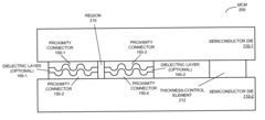
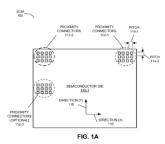
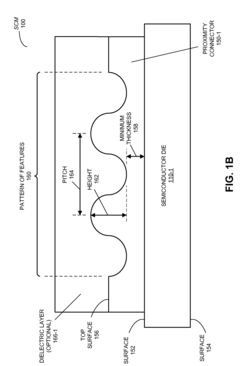
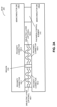
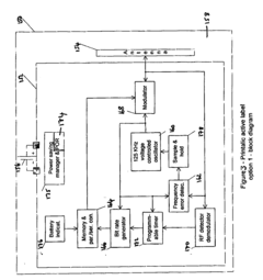
Capactive connectors with enhanced capacitive coupling
PatentActiveUS7863743B1
Innovation
- A single-chip module (SCM) with a pad featuring a pattern of raised elements that increase capacitance, and a multi-chip module (MCM) with interdigited pads, both utilizing a dielectric layer to enhance capacitive coupling, thereby increasing the effective area and reducing spacing between connectors.
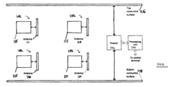
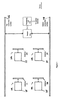
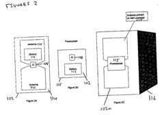
Active capacitive coupling RFID device, system and method of production thereof
PatentInactiveUS20070024425A1
Innovation
- An active RFID system employing capacitive coupling with a transponder that includes a power source, electronic circuitry, and an antenna, allowing for two-way communication on a single frequency, where the transponder and reader communicate on separate time slots, and the antenna can be printed using low-cost conductive materials like carbon ink.
Materials Science Advancements for Flexible Electronics
The evolution of flexible electronics has been fundamentally driven by breakthroughs in materials science. Traditional rigid electronic substrates like silicon and glass have given way to flexible polymers such as polyimide, polyethylene terephthalate (PET), and polydimethylsiloxane (PDMS), enabling bendable and stretchable electronic devices. These materials provide the necessary mechanical flexibility while maintaining electrical performance under deformation conditions.
Recent advancements in conductive materials have addressed the critical challenge of maintaining electrical conductivity during bending and stretching. Silver nanowires, carbon nanotubes, and graphene have emerged as promising alternatives to conventional metal films, offering superior flexibility and conductivity. Particularly noteworthy is the development of liquid metal alloys based on gallium, which maintain conductivity even under extreme deformation, making them ideal for applications requiring high flexibility.
Dielectric materials play a crucial role in capacitive coupling effects in flexible electronics. Novel high-k dielectric materials with maintained performance during mechanical deformation have been developed to enhance capacitive coupling while minimizing parasitic effects. These materials include modified versions of aluminum oxide, hafnium oxide, and various polymer-ceramic composites that maintain their dielectric properties under strain.
Interface engineering between different material layers has become increasingly important for managing capacitive coupling. Research has focused on creating seamless interfaces that minimize impedance mismatches and reduce parasitic capacitance. Surface modification techniques, including plasma treatment and self-assembled monolayers, have proven effective in optimizing these interfaces for improved signal integrity.
Encapsulation materials have evolved significantly to protect flexible electronic components while minimizing their impact on capacitive coupling. Thin-film barrier materials with multiple alternating organic and inorganic layers provide excellent protection against environmental factors while maintaining the flexibility of the overall device. These materials effectively isolate sensitive components from external electromagnetic interference that could disrupt capacitive coupling.
Emerging materials like MXenes (two-dimensional transition metal carbides and nitrides) show exceptional promise for flexible electronics applications due to their unique combination of metallic conductivity and hydrophilicity. Their tunable surface terminations allow for precise control of capacitive coupling effects, potentially enabling more efficient and reliable flexible electronic systems.
Manufacturing Process Optimization for Coupling Reduction
Optimizing manufacturing processes is critical for reducing capacitive coupling effects in flexible electronics. Current manufacturing techniques often introduce unintended coupling due to material inconsistencies, alignment errors, and process variations. Advanced lithography techniques with sub-micron precision can significantly reduce parasitic capacitance by ensuring precise patterning of conductive traces with optimal separation distances.
Material selection plays a crucial role in coupling reduction. By implementing multi-layer dielectric structures with carefully controlled thicknesses and dielectric constants, manufacturers can create effective isolation barriers between signal paths. Recent developments in low-k dielectric materials specifically engineered for flexible substrates have demonstrated up to 40% reduction in cross-talk compared to traditional materials.
Process temperature control represents another optimization frontier. Maintaining precise thermal profiles during deposition and curing processes prevents material expansion and contraction that can lead to misalignment and variable coupling effects. Implementation of real-time temperature monitoring systems with feedback control loops has shown to improve coupling consistency by 25-30% across production batches.
Surface treatment technologies have emerged as effective coupling mitigation strategies. Plasma treatment processes that modify the surface energy of substrates before conductor deposition improve adhesion while creating more uniform interfaces with predictable electrical characteristics. These treatments, when combined with specialized encapsulation techniques, create more stable electrical environments that resist environmental factors known to exacerbate coupling.
Roll-to-roll manufacturing optimization presents unique challenges for coupling reduction. Tension control systems with advanced feedback mechanisms help maintain consistent substrate dimensions throughout the process. Web handling innovations that reduce substrate deformation during processing have demonstrated significant improvements in maintaining designed spacing between conductive elements.
Post-production tuning methods offer additional coupling reduction opportunities. Laser trimming techniques can fine-tune critical dimensions after initial manufacturing, while selective application of dielectric overlays can provide targeted isolation where coupling effects are most problematic. These approaches allow for remediation of coupling issues identified during electrical testing.
Quality control integration throughout the manufacturing process is essential for coupling reduction. Implementing in-line impedance testing and capacitance mapping enables real-time detection of coupling anomalies. Advanced optical inspection systems with machine learning algorithms can identify potential coupling issues before they manifest in electrical performance, allowing for immediate process adjustments.
Unlock deeper insights with Patsnap Eureka Quick Research — get a full tech report to explore trends and direct your research. Try now!
Generate Your Research Report Instantly with AI Agent
Supercharge your innovation with Patsnap Eureka AI Agent Platform!