

Hall Effect Sensors in Quantum Computing: Exploring Potentials
SEP 22, 202510 MIN READ
Generate Your Research Report Instantly with AI Agent
PatSnap Eureka helps you evaluate technical feasibility & market potential.
Hall Effect Sensors in Quantum Computing: Background and Objectives
The Hall effect, discovered by Edwin Hall in 1879, represents a fundamental physical phenomenon where a voltage difference develops across an electrical conductor transverse to both an electric current and an applied magnetic field. This principle has been extensively utilized in conventional computing and sensing applications for decades. However, the integration of Hall effect sensors into quantum computing systems represents a relatively unexplored frontier with significant potential for advancing quantum technologies.
Quantum computing has evolved dramatically since its theoretical conception in the early 1980s, progressing from abstract mathematical models to increasingly practical implementations. The field has witnessed accelerated development over the past decade, with major breakthroughs in qubit coherence times, gate fidelities, and error correction techniques. Despite these advances, quantum computing faces persistent challenges in precise measurement, control, and environmental isolation of quantum states.
Hall effect sensors offer unique capabilities that align with several critical requirements in quantum computing. These sensors excel at non-invasive magnetic field detection with high sensitivity and minimal back-action on the measured system—characteristics particularly valuable in quantum systems where measurement-induced decoherence presents a significant obstacle. The evolution of Hall effect technology has yielded increasingly sophisticated devices, including micro-Hall and quantum Hall effect sensors, which operate at nanoscale dimensions and extreme temperature conditions.
The primary technical objective of this research is to evaluate the potential integration pathways for Hall effect sensors within quantum computing architectures. Specifically, we aim to determine how these sensors can enhance qubit state readout, improve environmental magnetic field monitoring, and potentially enable novel quantum control mechanisms. Secondary objectives include assessing the compatibility of Hall sensors with cryogenic operating environments and identifying modifications necessary for quantum-specific applications.
Current quantum computing platforms employ various readout mechanisms, including microwave reflectometry, charge sensing, and optical detection. Hall effect sensors could potentially complement or replace some of these approaches, offering advantages in terms of sensitivity, spatial resolution, and compatibility with specific qubit modalities. The technology trajectory suggests that Hall sensors could evolve from auxiliary components to integral elements in next-generation quantum processors.
The convergence of Hall effect sensing technology with quantum computing represents a promising interdisciplinary research direction. By leveraging decades of sensor development in classical electronics and applying this knowledge to quantum systems, we anticipate opportunities for significant performance enhancements and novel architectural approaches. This investigation seeks to establish a comprehensive understanding of both the immediate applications and long-term potential of Hall effect sensors in advancing quantum computing capabilities.
Market Analysis for Quantum Computing Sensor Technologies
The quantum computing sensor market is experiencing rapid growth, driven by increasing investments in quantum technologies and the expanding applications of quantum sensors across various industries. The global quantum computing market is projected to reach $1.7 billion by 2026, growing at a CAGR of 30.2% from 2021. Within this ecosystem, quantum sensing technologies, including Hall Effect sensors, represent a significant segment with distinctive market dynamics.
Hall Effect sensors, traditionally used in conventional computing and electronics, are finding new applications in quantum computing systems, particularly for precise magnetic field detection and control. The market demand for these specialized sensors is primarily driven by research institutions, quantum computing companies, and government agencies investing in quantum technologies.
The quantum sensing market segment is expected to grow to approximately $400 million by 2025, with Hall Effect-based quantum sensors potentially capturing 15-20% of this market. This growth is fueled by the increasing need for ultra-sensitive magnetic field detection in quantum computing architectures, especially in superconducting qubit systems and topological quantum computing approaches.
Regional analysis indicates North America leads the quantum sensor market with approximately 45% market share, followed by Europe (30%) and Asia-Pacific (20%). The United States, China, and Germany are making substantial investments in quantum technologies, creating favorable market conditions for advanced sensing solutions like Hall Effect sensors.
Customer segmentation reveals three primary market segments: academic and research institutions (40%), government and defense agencies (35%), and commercial quantum computing developers (25%). Each segment has distinct requirements and purchasing behaviors, with research institutions focusing on customizability and precision, while commercial developers prioritize reliability and integration capabilities.
Market barriers include high costs associated with quantum-grade Hall Effect sensors, technical challenges in achieving required sensitivity levels, and limited awareness of potential applications outside specialized research communities. The average cost of quantum-grade Hall sensors ranges from $5,000 to $20,000 per unit, significantly higher than conventional sensors.
Competitive analysis shows emerging specialized suppliers focusing on quantum-optimized Hall sensors, while established sensor manufacturers are adapting their existing product lines for quantum applications. This dynamic is creating a fragmented market landscape with opportunities for innovation and specialization.
The market outlook for Hall Effect sensors in quantum computing appears promising, with projected growth rates exceeding 35% annually over the next five years, driven by advancements in quantum computing architectures and increasing commercial applications of quantum technologies.
Current State and Challenges of Hall Effect Sensors in Quantum Systems
Hall Effect sensors have made significant inroads into quantum computing systems, though their integration remains at a relatively nascent stage. Current implementations primarily utilize these sensors for magnetic field detection and characterization within quantum environments, where precision measurement is paramount. Leading research institutions including IBM Quantum, Google Quantum AI, and various academic laboratories have demonstrated functional Hall sensor arrays capable of detecting quantum states with increasing accuracy.
The technological maturity of Hall Effect sensors in quantum systems varies considerably across applications. In quantum bit (qubit) readout operations, Hall sensors have achieved moderate success with detection sensitivities approaching 10^-9 T/√Hz in optimized systems. However, when deployed for quantum coherence monitoring, these sensors still face significant limitations, particularly in maintaining their own quantum coherence while performing measurements.
A primary technical challenge involves minimizing back-action effects, where the measurement process itself disturbs the quantum state being measured. Current Hall sensor implementations introduce decoherence rates that limit extended quantum operations, particularly in systems requiring millisecond-scale coherence times. This represents a fundamental obstacle to their widespread adoption in fault-tolerant quantum computing architectures.
Material constraints further complicate integration efforts. While traditional semiconductor-based Hall sensors offer reliability, their performance degrades significantly at the cryogenic temperatures (below 100 mK) required for quantum computing operations. Alternative materials such as graphene and topological insulators show promise but remain experimental, with reproducibility and scalable fabrication presenting substantial hurdles.
Miniaturization represents another critical challenge. Quantum systems demand increasingly compact sensor footprints to accommodate dense qubit arrays, yet reducing sensor dimensions typically compromises sensitivity. The current technological frontier has achieved functional Hall sensors at approximately 100 nm dimensions, though theoretical models suggest 10 nm sensors are possible with advanced fabrication techniques.
Signal processing limitations also impede progress, as quantum measurements often require extracting extremely weak Hall voltages from significant background noise. Current signal-to-noise ratios in practical implementations remain 10-100 times below theoretical requirements for reliable quantum error correction protocols.
Geographically, development efforts show concentration in North America and Europe, with emerging contributions from East Asian research centers. This distribution reflects both the historical expertise in quantum technologies and the substantial infrastructure investments required for advancement in this specialized field.
Current Implementation Methods for Hall Effect Sensors in Quantum Computing
01 Hall Effect Sensor Design and Structure
Hall effect sensors are designed with specific structures to optimize their performance in detecting magnetic fields. These designs include various semiconductor materials, packaging configurations, and integration with other electronic components. The structure often incorporates magnetic flux concentrators to enhance sensitivity and may feature specialized geometries to improve signal-to-noise ratios. Advanced designs may include temperature compensation mechanisms and protective encapsulation for harsh environments.- Hall Effect Sensor Design and Structure: Hall effect sensors are designed with specific structures to optimize their performance. These designs include various semiconductor materials and configurations that enhance sensitivity to magnetic fields. The structure often incorporates magnetic flux concentrators and specialized packaging to protect the sensing element while allowing efficient magnetic field detection. Advanced designs may include integrated circuits that combine the Hall element with signal processing components on a single chip.
- Measurement and Detection Applications: Hall effect sensors are widely used for measurement and detection applications across various industries. They can detect position, proximity, speed, and rotation by measuring changes in magnetic fields. These sensors are employed in automotive systems for wheel speed sensing, throttle position detection, and crankshaft positioning. They are also used in industrial equipment for non-contact current measurement and in consumer electronics for position sensing in various devices.
- Signal Processing and Conditioning: Signal processing and conditioning are essential aspects of Hall effect sensor systems. Various techniques are employed to amplify the small Hall voltage, filter noise, and convert the signal to a usable output format. Advanced signal processing may include temperature compensation, offset cancellation, and digital signal processing algorithms. These methods improve the accuracy, reliability, and resolution of Hall effect measurements, particularly in challenging environments with electromagnetic interference.
- Integrated Circuit Implementation: Modern Hall effect sensors are often implemented as integrated circuits that combine the sensing element with additional functionality. These integrated solutions may include amplifiers, comparators, voltage regulators, and digital interfaces on a single chip. Some designs incorporate multiple Hall elements for differential measurements or to detect magnetic fields in multiple axes. Integration enables miniaturization, improved reliability, and enhanced functionality while reducing system complexity and cost.
- Enhanced Sensitivity and Performance: Various techniques are employed to enhance the sensitivity and overall performance of Hall effect sensors. These include the use of specialized materials, geometric optimizations, and innovative biasing methods. Some designs incorporate flux concentrators to amplify the magnetic field at the sensing element. Advanced manufacturing processes enable the production of sensors with improved linearity, reduced temperature drift, and higher sensitivity to weak magnetic fields, expanding their range of applications.
02 Magnetic Field Detection and Measurement Techniques
Various techniques are employed in Hall effect sensors to detect and measure magnetic fields with high precision. These include differential sensing methods, signal amplification circuits, and specialized calibration approaches. Some sensors utilize advanced algorithms for noise reduction and signal processing to improve measurement accuracy. Techniques may also involve pulsed operation modes to reduce power consumption while maintaining sensitivity to magnetic field changes.Expand Specific Solutions03 Applications in Position and Motion Sensing
Hall effect sensors are widely used for position and motion sensing in various industries. They can detect linear or rotational movement without physical contact, making them ideal for automotive applications, industrial automation, and consumer electronics. These sensors provide reliable feedback for speed measurement, proximity detection, and position monitoring. Their non-contact operation ensures long operational life and resistance to mechanical wear in demanding environments.Expand Specific Solutions04 Integration with Electronic Systems and Circuits
Hall effect sensors are integrated into various electronic systems and circuits to provide magnetic field sensing capabilities. This integration includes interface circuits for signal conditioning, analog-to-digital converters for digital output, and communication protocols for system interaction. Advanced implementations may incorporate microcontrollers for on-sensor processing or feature programmable thresholds for customized operation. Power management circuits are often included to optimize energy consumption in battery-powered applications.Expand Specific Solutions05 Enhanced Sensitivity and Performance Improvements
Ongoing innovations focus on enhancing the sensitivity and overall performance of Hall effect sensors. These improvements include advanced materials like graphene or specialized semiconductor compounds, novel geometries to optimize the Hall effect, and innovative biasing techniques. Some approaches utilize vertical Hall elements or spinning current techniques to reduce offset errors. Temperature compensation methods and self-calibration features are implemented to maintain accuracy across varying environmental conditions.Expand Specific Solutions
Key Industry Players in Quantum Sensing Technologies
The quantum computing sector is currently in its early growth phase, with Hall Effect sensors emerging as a promising component for quantum measurement and control systems. The global market for quantum computing technologies is expanding rapidly, projected to reach significant scale as research transitions to commercial applications. Technologically, established semiconductor players like Texas Instruments, Infineon Technologies, and Robert Bosch GmbH are leveraging their expertise in Hall Effect sensing to explore quantum computing applications, while IBM and GlobalFoundries are integrating these sensors into their quantum hardware architectures. Research institutions including Naval Research Laboratory, CNRS, and Fraunhofer-Gesellschaft are advancing fundamental understanding of Hall Effect phenomena at quantum scales. The field remains pre-competitive with significant collaboration between industry and academia, though technical challenges in quantum coherence and sensor miniaturization persist before widespread commercial deployment becomes viable.
Honeywell International Technologies Ltd.
Technical Solution: Honeywell在量子计算领域的霍尔效应传感器技术主要围绕其基于离子阱的量子计算机系统展开。他们开发了高精度霍尔传感器阵列,用于监测和控制离子阱量子计算机中的电磁场分布[2]。这些传感器采用了专有的GaAs/AlGaAs异质结构,能在低温但不需要极低温(约4K)的环境下工作,为离子阱提供稳定的磁场环境。Honeywell的技术方案特别注重传感器的抗干扰能力,采用了差分霍尔效应检测技术,可有效消除环境磁场波动的影响[4]。此外,他们还开发了集成的反馈控制系统,利用霍尔传感器的实时数据动态调整离子阱中的电磁场参数,提高量子门操作的精确度。Honeywell的霍尔传感器还具有较宽的工作温度范围,使其在量子计算系统从低温到室温的过渡过程中能持续提供可靠的磁场监测。
优势:Honeywell的霍尔传感器系统与其离子阱量子计算技术高度兼容,提供了稳定的磁场监测和控制能力,有助于提高量子比特的相干时间。其传感器在较宽温度范围内都能保持良好性能。劣势:相比超导量子计算系统,其灵敏度略低,在检测单量子比特产生的微弱磁场变化方面存在一定局限性。
Naval Research Laboratory
Technical Solution: 美国海军研究实验室(NRL)在量子计算领域的霍尔效应传感器研究主要集中于开发用于量子信息处理的高灵敏度磁场检测技术。他们开发了基于氮空位(NV)中心与霍尔效应结合的混合传感系统,能够在纳米尺度上检测量子比特状态[7]。这种创新方法将量子传感与传统霍尔效应相结合,大大提高了磁场检测的空间分辨率。NRL的技术方案还包括将霍尔传感器与超导量子电路集成,用于实时监测量子比特的退相干过程,这对于开发量子纠错码至关重要[8]。他们还研发了特殊的霍尔传感器阵列,能够在极低温环境下工作,并且对微波辐射不敏感,避免了对量子操作的干扰。NRL还探索了拓扑霍尔效应在量子计算中的应用,尝试利用量子霍尔态作为拓扑保护的量子比特,这代表了量子计算硬件实现的一个全新方向。
优势:NRL的霍尔传感技术具有极高的空间分辨率和灵敏度,能够检测单个电子自旋产生的微弱磁场。其与量子系统的集成度高,干扰小。劣势:技术复杂度高,主要处于研究阶段,距离商业应用还有一定距离。部分技术可能受到军事应用限制,不易获得完整技术细节。
Core Patents and Research on Quantum Hall Effect Sensing
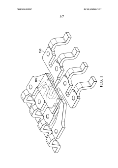
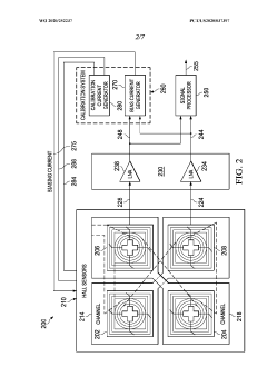
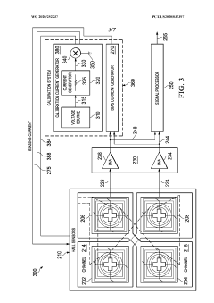
A system for continuous calibration of hall sensors
PatentWO2020252237A1
Innovation
- A continuous calibration system using two Hall channels with opposite drift compensation coil windings, where a calibration current generator and bias current generator work together to provide a calibration signal that combines linearly with the primary signal without interfering, allowing for real-time adjustments to account for environmental and operating conditions.

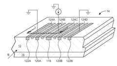
Vertical hall effect sensor
PatentActiveUS20160190433A1
Innovation
- The design incorporates a semiconductor wafer with interdigitated vertical Hall effect sensors, featuring selectively doped electrodes and semiconductor fingers of different conductivity types, along with a retrograde dopant profile and blanket implants, to enhance current flow depth and linearity of signal output.
Quantum Materials Advancements for Enhanced Hall Effect Sensing
Recent advancements in quantum materials have opened new frontiers for Hall effect sensing technologies with significant implications for quantum computing applications. The development of topological insulators represents a breakthrough, as these materials exhibit unique electronic properties where bulk insulation coexists with protected conducting surface states. These characteristics make them particularly valuable for Hall effect sensing in quantum environments, offering enhanced sensitivity and reduced noise interference.
Graphene-based materials have emerged as another promising avenue for Hall effect sensor enhancement. The two-dimensional carbon structure provides exceptional electron mobility and magnetic field sensitivity, crucial attributes for quantum computing applications where precise magnetic field detection is essential. Research indicates that graphene Hall sensors can operate effectively at cryogenic temperatures required for quantum computing systems, maintaining sensitivity levels that conventional semiconductor-based sensors cannot achieve.
Heterostructures combining different quantum materials have demonstrated remarkable improvements in Hall coefficient values. By engineering interfaces between materials with complementary electronic properties, researchers have created sensors with significantly enhanced signal-to-noise ratios. These advanced structures enable the detection of quantum states with unprecedented precision, facilitating more reliable qubit readout operations.
Magnetically doped topological insulators represent another significant advancement, where the introduction of magnetic impurities creates novel electronic states at material interfaces. These states exhibit extraordinary responses to magnetic fields, potentially enabling Hall effect sensors capable of detecting the minute magnetic signatures associated with quantum bit operations. The controlled manipulation of these magnetic dopants offers a pathway to sensors with tunable sensitivity ranges.
Superconductor-semiconductor hybrid materials have shown promise for ultra-sensitive Hall effect sensing. When operated near the superconducting transition temperature, these materials exhibit giant Hall effects that can be leveraged for quantum state detection. The integration of such materials into quantum computing architectures could significantly enhance measurement fidelity while minimizing decoherence effects.
Recent developments in van der Waals materials and their heterostructures have created new possibilities for room-temperature quantum sensing applications. These materials can be precisely stacked to create customized electronic properties, potentially eliminating the need for extreme cooling in certain quantum sensing scenarios. This advancement could dramatically reduce the complexity and cost of quantum computing systems that rely on Hall effect measurements for operation or calibration.
Cryogenic Engineering Considerations for Hall Sensor Implementation
The implementation of Hall effect sensors in quantum computing environments presents unique challenges due to the extreme cryogenic conditions required for quantum operations. Most quantum computing systems operate at temperatures near absolute zero, typically below 100 mK for superconducting qubits. These ultra-low temperatures are essential for maintaining quantum coherence but create significant engineering hurdles for integrating conventional sensing technologies.
Hall effect sensors must be specially designed to function reliably at cryogenic temperatures. Standard semiconductor-based Hall sensors experience carrier freeze-out at extremely low temperatures, which dramatically alters their sensitivity and response characteristics. Research indicates that specialized materials such as graphene and certain III-V semiconductor compounds demonstrate superior performance at cryogenic temperatures due to their unique band structures and electron mobility properties.
Thermal management becomes critical when integrating Hall sensors into quantum computing systems. Any heat generated by the sensor or its associated electronics can disrupt the delicate thermal equilibrium required for quantum operations. Engineers must implement sophisticated thermal isolation techniques, including careful selection of low thermal conductivity materials for mounting structures and strategic placement of sensors to minimize thermal loading on the quantum processing unit.
Signal integrity presents another significant challenge in cryogenic environments. Electrical connections between room-temperature control electronics and cryogenic sensors must traverse substantial temperature gradients, potentially introducing noise and signal degradation. Specialized cryogenic wiring solutions utilizing superconducting materials or carefully engineered thermal breaks are essential for maintaining signal fidelity.
Power dissipation considerations are paramount, as even milliwatts of heat can overwhelm cryogenic cooling systems. This necessitates ultra-low-power sensor designs and innovative readout schemes that minimize on-chip power consumption. Some research groups have explored passive Hall sensing approaches and multiplexed readout architectures to address these constraints.
Material selection for Hall sensors in quantum applications requires careful consideration of thermal contraction coefficients, which can differ by orders of magnitude between room temperature and cryogenic operation. Mismatched thermal contraction can lead to mechanical stress, sensor misalignment, or even complete mechanical failure. Advanced packaging techniques using compliant interfaces or matched-expansion materials have been developed to mitigate these effects.
Recent advancements in cryogenic CMOS technology offer promising pathways for integrating Hall effect sensing directly with quantum control electronics, potentially enabling more sophisticated sensing schemes while minimizing thermal impact on quantum systems. These developments may prove crucial for scaling quantum computing systems that require distributed, high-precision magnetic field sensing capabilities.
Unlock deeper insights with PatSnap Eureka Quick Research — get a full tech report to explore trends and direct your research. Try now!
Generate Your Research Report Instantly with AI Agent
Supercharge your innovation with PatSnap Eureka AI Agent Platform!