Design Considerations for Hall Effect Sensors in Large-Scale Deployments
SEP 22, 20259 MIN READ
Generate Your Research Report Instantly with AI Agent
Patsnap Eureka helps you evaluate technical feasibility & market potential.
Hall Effect Sensor Technology Background and Objectives
Hall Effect sensors, discovered by Edwin Hall in 1879, have evolved from simple magnetic field detection devices to sophisticated components integral to modern electronic systems. These sensors operate on the principle of the Hall Effect, where a voltage difference is generated across an electrical conductor transverse to an electric current when exposed to a magnetic field. This fundamental principle has remained unchanged, while the implementation technology has advanced significantly over the decades.
The evolution of Hall Effect sensors has been marked by several key technological milestones. Early implementations in the mid-20th century were bulky and limited in sensitivity. The semiconductor revolution in the 1970s enabled the miniaturization of these sensors, leading to their integration into various industrial applications. The 1990s saw further advancements with the development of integrated circuits incorporating Hall Effect elements, significantly enhancing their functionality and reliability.
Recent technological trends in Hall Effect sensors include increased sensitivity, reduced power consumption, and enhanced integration capabilities. Modern sensors can detect magnetic fields in the microtesla range, operate on milliwatt power levels, and often include on-chip signal processing capabilities. The miniaturization trend continues, with some sensors now available in packages smaller than 2mm², facilitating their deployment in space-constrained applications.
For large-scale deployments, the objectives of Hall Effect sensor technology focus on several critical aspects. Scalability is paramount, requiring sensors that can be mass-produced with consistent performance characteristics. Reliability under varied environmental conditions is essential, as large deployments may span diverse operating environments. Energy efficiency becomes increasingly important when multiplied across thousands of units, driving the development of ultra-low-power variants.
Connectivity represents another key objective, with modern deployments requiring sensors that can integrate seamlessly with IoT networks and cloud-based monitoring systems. This has led to the development of Hall Effect sensors with built-in communication protocols such as I²C, SPI, or wireless capabilities. Data processing capabilities at the edge are also becoming increasingly important to reduce bandwidth requirements and enable real-time decision making.
The technical goals for next-generation Hall Effect sensors in large deployments include achieving sub-microtesla sensitivity while maintaining stability across temperature ranges from -40°C to +125°C. Power consumption targets are pushing below 10μW during active sensing, with sleep-mode consumption in the nanowatt range. Durability objectives include operational lifespans exceeding 10 years in industrial environments, with mean time between failures (MTBF) ratings above 1 million hours.
Market Demand Analysis for Large-Scale Hall Sensor Applications
The global market for Hall Effect sensors in large-scale deployments has experienced significant growth over the past decade, primarily driven by increasing automation across multiple industries. Current market analysis indicates that the automotive sector remains the largest consumer of Hall Effect sensors, accounting for approximately 35% of the total market share. This dominance stems from the expanding use of these sensors in advanced driver assistance systems (ADAS), electric vehicle battery management, and position sensing applications.
Industrial automation represents the second-largest market segment, with manufacturing facilities increasingly adopting Hall Effect sensors for precise position detection, speed monitoring, and current measurement. The transition toward Industry 4.0 and smart manufacturing has accelerated demand, as these sensors provide reliable non-contact measurement capabilities essential for automated production environments.
Consumer electronics constitutes another rapidly growing sector, with Hall Effect sensors being integrated into smartphones, tablets, and wearable devices for functions ranging from lid detection to compass applications. The miniaturization trend in consumer electronics has pushed manufacturers to develop increasingly compact Hall sensor solutions without compromising performance.
Market research reveals that large-scale deployments of Hall Effect sensors face specific demands that differ from small-scale applications. These include requirements for enhanced durability under harsh environmental conditions, improved energy efficiency for battery-powered applications, and cost-effectiveness when deployed in thousands of units. Additionally, there is growing demand for sensors with digital interfaces and networking capabilities to support IoT integration.
Regional analysis shows North America and Europe currently leading in Hall sensor adoption for industrial applications, while Asia-Pacific demonstrates the fastest growth rate, particularly in automotive and consumer electronics sectors. China's manufacturing sector alone has increased its Hall sensor consumption by nearly 28% annually over the past three years.
Future market projections indicate that the demand for Hall Effect sensors in large-scale deployments will continue to grow at a compound annual growth rate of 8.7% through 2028. This growth will be particularly pronounced in emerging applications such as renewable energy systems, smart city infrastructure, and advanced healthcare equipment. The renewable energy sector specifically shows promise as solar tracking systems and wind turbines increasingly utilize Hall sensors for position feedback and current monitoring.
Customer requirements analysis reveals a clear trend toward multi-functional sensor solutions that combine Hall Effect sensing with other measurement capabilities in integrated packages. This trend is driven by the need to reduce component count, simplify installation, and lower overall system costs in large-scale deployments.
Current Technical Challenges in Hall Effect Sensor Deployments
Hall effect sensors face significant challenges in large-scale deployments across various industrial and commercial applications. One of the primary technical hurdles is maintaining consistent sensitivity across temperature variations. When deployed in environments with fluctuating temperatures, these sensors often exhibit drift in their output characteristics, leading to measurement inaccuracies. This is particularly problematic in outdoor installations or industrial settings where temperature gradients can be substantial throughout operational cycles.
Signal-to-noise ratio degradation presents another major challenge, especially in environments with electromagnetic interference (EMI). Large-scale deployments frequently place sensors near power lines, motors, or other electrical equipment that generate magnetic fields, compromising measurement integrity. Current shielding solutions add bulk and cost, making them impractical for high-density sensor networks.
Power consumption remains a critical constraint, particularly for battery-operated or energy-harvesting sensor nodes in remote locations. While low-power Hall effect sensors exist, they typically sacrifice performance parameters such as response time or sensitivity. This trade-off becomes increasingly problematic as deployment scales increase, necessitating more frequent maintenance interventions.
Miniaturization challenges persist despite advances in semiconductor manufacturing. As deployments grow, spatial constraints become more pressing, yet reducing sensor size often impacts magnetic field detection capabilities. The current generation of sensors struggles to maintain performance metrics when scaled down beyond certain thresholds, limiting installation options in space-constrained applications.
Calibration and drift compensation represent significant operational challenges in large networks. Each sensor requires individual calibration to account for manufacturing variations, and this calibration tends to degrade over time. Current automated calibration methods are insufficient for maintaining measurement accuracy across thousands of sensors without substantial maintenance overhead.
Integration with existing infrastructure poses compatibility issues, particularly regarding signal processing and data transmission protocols. Many large-scale deployments must interface with legacy systems that weren't designed for the data volumes generated by modern sensor networks. The resulting bottlenecks in data processing and transmission can undermine the benefits of comprehensive sensor coverage.
Reliability and mean time between failures (MTBF) metrics become increasingly critical as deployment scale increases. Current Hall effect sensors exhibit varying failure rates depending on environmental conditions, with moisture ingress and mechanical stress being common failure modes. The statistical probability of sensor failures increases proportionally with deployment size, creating maintenance challenges that current predictive failure models inadequately address.
Current Implementation Solutions for Large-Scale Deployments
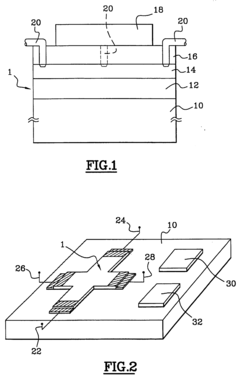
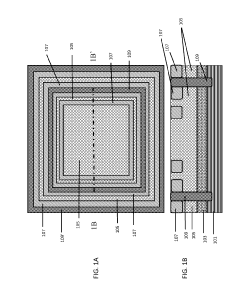
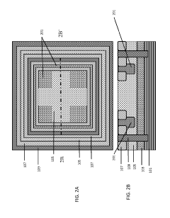
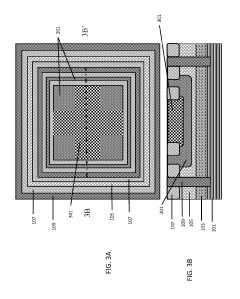
01 Hall Effect Sensor Design and Structure
Hall effect sensors are designed with specific structures to detect magnetic fields. These designs include various semiconductor materials and configurations to optimize sensitivity and performance. The structure typically includes a thin semiconductor layer with electrical contacts for current input and voltage measurement. Advanced designs may incorporate multiple sensing elements or specialized geometries to enhance detection capabilities.- Hall Effect Sensor Design and Structure: Hall effect sensors are designed with specific structures to optimize their performance. These designs include various semiconductor materials and configurations that enhance sensitivity to magnetic fields. The structure typically includes a thin semiconductor layer with electrical contacts for current input and voltage measurement. Advanced designs may incorporate multiple sensing elements or specialized geometries to improve directional sensitivity and reduce interference.
- Magnetic Field Detection and Measurement: Hall effect sensors operate by detecting magnetic fields through the Hall effect principle, where a voltage is generated perpendicular to both the current flow and magnetic field. These sensors can measure field strength, direction, and variations with high precision. Applications include position sensing, speed detection, and current measurement. Various techniques are employed to enhance sensitivity and reduce noise in magnetic field measurements.
- Integration with Electronic Systems: Hall effect sensors are integrated into various electronic systems for sensing and control applications. They can be incorporated into integrated circuits with signal processing capabilities, allowing for direct digital output. These sensors interface with microcontrollers and other electronic components to provide real-time feedback for system control. Integration techniques focus on minimizing size while maintaining performance and reliability in diverse operating environments.
- Enhanced Sensitivity and Calibration Methods: Various techniques are employed to enhance the sensitivity of Hall effect sensors and ensure accurate measurements. These include specialized amplification circuits, temperature compensation methods, and advanced calibration techniques. Sensor designs may incorporate offset cancellation, chopper stabilization, or spinning current techniques to reduce drift and improve accuracy. Calibration methods ensure consistent performance across manufacturing variations and operating conditions.
- Application-Specific Hall Sensor Implementations: Hall effect sensors are customized for specific applications with unique requirements. Automotive applications may focus on robustness and reliability under harsh conditions. Industrial implementations might prioritize high precision and long-term stability. Consumer electronics applications typically emphasize miniaturization and low power consumption. Each implementation involves specific design considerations to optimize performance for the intended use case.
02 Magnetic Field Detection and Measurement Applications
Hall effect sensors are widely used for detecting and measuring magnetic fields in various applications. They can accurately determine the strength and direction of magnetic fields, making them valuable in position sensing, speed detection, and current measurement systems. These sensors provide non-contact measurement capabilities, allowing for reliable operation in harsh environments where mechanical sensors might fail.Expand Specific Solutions03 Integrated Circuit Implementation and Signal Processing
Modern Hall effect sensors are often implemented as integrated circuits that combine the sensing element with signal conditioning and processing capabilities. These integrated solutions may include amplifiers, temperature compensation circuits, and digital interfaces. Advanced signal processing techniques help improve accuracy, reduce noise, and enable features such as programmable thresholds or digital output formats.Expand Specific Solutions04 Enhanced Sensitivity and Interference Reduction
Techniques for improving Hall effect sensor sensitivity and reducing interference are critical for high-performance applications. These include specialized materials, geometric optimizations, and shielding methods. Chopper stabilization, spinning current techniques, and differential sensing approaches are employed to minimize offset errors and temperature drift. These enhancements allow for detection of weaker magnetic fields and operation in electromagnetically noisy environments.Expand Specific Solutions05 Automotive and Industrial Applications
Hall effect sensors find extensive use in automotive and industrial applications due to their reliability and durability. They are employed in wheel speed sensors, throttle position sensors, current monitoring systems, and motor control applications. In industrial settings, they serve in proximity detection, flow meters, and security systems. Their non-contact operation and resistance to environmental factors make them ideal for these demanding applications.Expand Specific Solutions
Key Industry Players in Hall Effect Sensor Manufacturing
The Hall Effect Sensor market is currently in a growth phase, with increasing adoption across automotive, industrial, and consumer electronics sectors. The global market size is estimated to reach approximately $2 billion by 2025, growing at a CAGR of 8-10%. Technologically, the field is maturing with key players like Infineon Technologies, Allegro MicroSystems, and Texas Instruments leading innovation in miniaturization and sensitivity improvements. Established industrial giants such as Robert Bosch, Honeywell, and Siemens are integrating these sensors into comprehensive systems solutions. The competitive landscape shows a mix of semiconductor specialists and diversified technology corporations, with recent advancements focusing on enhanced temperature stability, reduced power consumption, and improved signal-to-noise ratios for large-scale deployments. Asian manufacturers like Nanjing Xinjie Zhongxu are rapidly gaining market share through cost-effective solutions.
Infineon Technologies AG
Technical Solution: Infineon's design approach for large-scale Hall effect sensor deployments centers on their TLE4966 and TLE4964 series, which incorporate integrated signal processing and temperature compensation circuits. Their solution includes dual-die redundancy architecture that enables fault detection capabilities with >99% diagnostic coverage[1]. For industrial and automotive applications, Infineon implements stress-resistant chip packaging with specialized molding compounds that can withstand temperatures from -40°C to +170°C while maintaining sensing accuracy within ±1.5%[2]. Their large-scale deployment strategy incorporates digital interfaces (SPI/I2C) with configurable addressing schemes allowing up to 32 sensors on a single bus, reducing wiring complexity in distributed sensing networks. Infineon's sensors feature programmable magnetic thresholds and hysteresis settings that can be calibrated post-installation via software, enabling remote configuration updates across deployed sensor networks without physical intervention[3].
Strengths: Superior temperature stability with integrated compensation circuits; advanced diagnostic capabilities through dual-die architecture; programmable thresholds allowing remote reconfiguration. Weaknesses: Higher power consumption compared to simpler Hall sensors; premium pricing may impact large-scale deployment economics; proprietary interfaces may require specialized integration knowledge.
Honeywell International Technologies Ltd.
Technical Solution: Honeywell's approach to large-scale Hall effect sensor deployments leverages their SS360/SS460 series with non-contact sensing technology designed specifically for harsh environments. Their solution incorporates solid-state reliability with MTBF (Mean Time Between Failures) exceeding 100 million operations[1], critical for minimizing maintenance in large installations. Honeywell implements a modular design philosophy with standardized form factors and interfaces, allowing for simplified installation and replacement across diverse deployment scenarios. Their sensors feature built-in EMC protection with immunity up to 10 V/m RF fields and 8kV ESD protection[2], addressing electromagnetic interference challenges in industrial environments. For power efficiency in large networks, Honeywell's sensors operate with supply voltages ranging from 3-24V with typical current draw under 4mA, supporting both battery-powered and wired deployments. Their design includes hermetically sealed packages with IP67/IP68 ratings, enabling deployment in outdoor and exposed locations without additional protective enclosures[3].
Strengths: Exceptional reliability metrics with high MTBF; wide operating voltage range supporting diverse power infrastructures; superior environmental protection with IP67/IP68 ratings. Weaknesses: Limited programmability compared to digital sensor variants; higher unit cost than simpler alternatives; larger physical footprint may constrain installation in space-limited applications.
Critical Patents and Technical Innovations in Hall Sensing
Hall-effect sensor and integrated circuit comprising such a sensor
PatentInactiveEP1091425A2
Innovation
- A Hall effect sensor structure with a thin active Si layer (less than 100 nm) and a SiO2 insulation layer, along with an insulating dielectric layer, which reduces temperature dependence and enhances magnetic field sensitivity, utilizing a quasi-two-dimensional electron gas and a guard electrode to minimize thermal effects.
Hall element for 3-d sensing and method for producing the same
PatentActiveUS20190259936A1
Innovation
- The development of a 3D Hall element with separate sensing for each magnetic field component, utilizing deep trench isolation (DTI) and shallow trench isolation (STI) regions, along with p-type and n-type wells, to optimize both planar and vertical Hall elements for improved sensitivity and reduced interference, compatible with CMOS technology nodes.
Environmental Impact and Sustainability Considerations
The environmental impact of Hall Effect sensors in large-scale deployments warrants careful consideration throughout their lifecycle. These sensors typically contain materials like gallium arsenide, indium antimonide, and various rare earth elements that require responsible sourcing and disposal. Mining these materials can lead to habitat disruption, water pollution, and significant carbon emissions. Organizations implementing large-scale sensor networks must therefore develop comprehensive procurement policies that prioritize suppliers with sustainable mining practices and transparent supply chains.
Manufacturing processes for Hall Effect sensors also present environmental challenges, particularly in terms of energy consumption and chemical usage. The semiconductor fabrication techniques employed typically require cleanroom environments with substantial energy demands for temperature and humidity control. Additionally, the etching and deposition processes utilize potentially harmful chemicals that necessitate proper handling and disposal protocols to prevent environmental contamination.
During the operational phase, Hall Effect sensors generally demonstrate favorable environmental characteristics compared to alternative sensing technologies. Their low power consumption contributes to reduced energy requirements in large-scale deployments, particularly when implemented with efficient power management systems. The long operational lifespan of properly designed Hall Effect sensors—often exceeding 10 years—further enhances their sustainability profile by minimizing replacement frequency and associated material consumption.
End-of-life considerations represent a critical aspect of environmental planning for large-scale sensor deployments. The electronic waste generated from decommissioned sensors contains valuable materials that can be recovered through proper recycling processes. Organizations should establish take-back programs and partner with certified e-waste recyclers to ensure responsible disposal and maximize material recovery rates. Design for disassembly principles should be incorporated early in the sensor development process to facilitate easier separation of components and materials at end-of-life.
Carbon footprint reduction strategies should be integrated throughout the deployment lifecycle. This includes optimizing transportation logistics during installation, implementing energy-efficient data transmission protocols, and utilizing renewable energy sources to power sensor networks where feasible. Life cycle assessment (LCA) methodologies can provide valuable insights into the environmental impacts across different deployment scenarios, enabling organizations to make data-driven decisions that minimize ecological harm while maintaining operational effectiveness.
Reliability and Longevity Testing Methodologies
Reliability and longevity testing for Hall Effect sensors in large-scale deployments requires comprehensive methodologies to ensure consistent performance throughout their operational lifetime. These testing approaches must account for the diverse environmental conditions and operational stresses that sensors will encounter in real-world applications.
Accelerated life testing (ALT) represents a cornerstone methodology, subjecting sensors to elevated stress levels to precipitate failures that might otherwise take years to manifest. For Hall Effect sensors, this typically involves temperature cycling between -40°C and 150°C, with dwell times calibrated to simulate thermal expansion and contraction stresses. Highly Accelerated Life Testing (HALT) extends this approach by combining multiple stressors simultaneously, including vibration, humidity, and voltage variations.
Environmental chamber testing forms another critical component, where sensors are exposed to controlled humidity (10-95% RH), salt spray conditions, and dust ingress scenarios. These tests are particularly relevant for Hall Effect sensors deployed in outdoor or industrial environments where contamination can interfere with magnetic field detection accuracy. Standardized testing protocols such as IP67/IP68 for water and dust resistance provide benchmarks for comparing sensor resilience.
Mechanical stress testing evaluates sensor robustness against physical forces, including shock testing (up to 1500g for automotive applications), vibration testing across frequency ranges typical in deployment environments (10-2000 Hz), and mounting stress simulations. These tests are essential as mechanical deformation can alter the magnetic properties and alignment critical to Hall Effect sensor operation.
Long-term drift analysis tracks sensor output stability over extended periods, typically 1000+ hours under constant conditions, to identify gradual performance degradation. This methodology is particularly important for Hall Effect sensors where magnetic sensitivity can change over time due to material aging or stress relaxation in packaging components.
Statistical reliability modeling complements physical testing by applying Weibull distribution analysis to failure data, enabling Mean Time Between Failures (MTBF) predictions. For large-scale deployments, this approach helps establish replacement schedules and maintenance protocols based on quantitative reliability metrics rather than reactive maintenance.
Field testing in actual deployment environments provides the ultimate validation, with sensors installed in pilot locations and monitored for 6-12 months. This methodology captures interaction effects between environmental factors that laboratory testing might miss, particularly important for Hall Effect sensors where magnetic interference from nearby systems can impact performance in ways difficult to simulate in isolation.
Unlock deeper insights with Patsnap Eureka Quick Research — get a full tech report to explore trends and direct your research. Try now!
Generate Your Research Report Instantly with AI Agent
Supercharge your innovation with Patsnap Eureka AI Agent Platform!