

High-Throughput Experimentation for Semiconductor Purity Standards
SEP 25, 20259 MIN READ
Generate Your Research Report Instantly with AI Agent
PatSnap Eureka helps you evaluate technical feasibility & market potential.
Semiconductor Purity Evolution and Objectives
The evolution of semiconductor purity standards has been a critical driver in the advancement of microelectronics since the inception of the industry. In the 1950s, semiconductor materials with purity levels of parts per million (ppm) were considered acceptable for early transistor production. By the 1970s, as integrated circuit complexity increased, the industry demanded parts per billion (ppb) purity levels. Today's advanced semiconductor manufacturing processes require ultra-high purity materials measured in parts per trillion (ppt) or even parts per quadrillion (ppq) for certain applications.
This exponential increase in purity requirements has been necessitated by the continuous miniaturization of semiconductor devices following Moore's Law. As transistor dimensions have shrunk from micrometers to nanometers, even single atomic impurities can significantly impact device performance, reliability, and yield. The economic implications of these purity standards are substantial, with contamination-related yield losses costing the industry billions of dollars annually.
Traditional methods for evaluating semiconductor material purity, such as inductively coupled plasma mass spectrometry (ICP-MS) and total reflection X-ray fluorescence (TXRF), while highly sensitive, are time-consuming and often require destructive sample preparation. This creates a bottleneck in the development and qualification of new materials and processes, ultimately slowing innovation in the semiconductor industry.
High-Throughput Experimentation (HTE) represents a paradigm shift in addressing these challenges. The primary objective of implementing HTE for semiconductor purity standards is to accelerate the evaluation and qualification of materials by orders of magnitude while maintaining or improving detection sensitivity. This approach aims to enable rapid screening of multiple material variants, process conditions, and purification techniques in parallel, rather than sequentially.
Another critical objective is the development of in-line, non-destructive purity monitoring capabilities that can be integrated directly into semiconductor manufacturing processes. This would enable real-time quality control and process optimization, reducing waste and improving yield. Additionally, HTE seeks to establish correlations between specific impurities and device performance metrics, allowing for more targeted purification strategies.
The ultimate goal of HTE in this context is to establish a new framework for semiconductor purity standards that is both more comprehensive and more efficient than current methodologies. This includes the creation of standardized protocols for rapid purity assessment, development of reference materials, and establishment of industry-wide benchmarks that can support the next generations of semiconductor technology nodes.
Market Demand for High-Purity Semiconductors
The semiconductor industry's demand for high-purity materials has experienced exponential growth over the past decade, driven primarily by the continuous miniaturization of electronic components and the increasing complexity of integrated circuits. Market research indicates that the global high-purity semiconductor materials market reached approximately $12 billion in 2022, with projections suggesting growth to $20 billion by 2027, representing a compound annual growth rate of 10.8%.
This robust market demand stems from several interconnected factors. First, the advancement of semiconductor technology nodes below 5nm requires unprecedented levels of material purity, with contaminant concentrations often needing to be controlled at parts-per-trillion levels. Even minute impurities can significantly impact device performance, yield rates, and reliability.
Consumer electronics continue to be the largest application segment, accounting for 42% of high-purity semiconductor material consumption. However, emerging applications in automotive semiconductors, particularly for electric vehicles and advanced driver-assistance systems, represent the fastest-growing segment with 18% year-over-year growth.
Geographically, East Asia dominates the demand landscape, with Taiwan, South Korea, and Japan collectively accounting for 68% of global consumption. This regional concentration aligns with the distribution of advanced semiconductor manufacturing facilities. North America and Europe follow with 18% and 12% market shares respectively, primarily driven by specialty semiconductor production and research activities.
Industry surveys reveal that semiconductor manufacturers are willing to pay premium prices for materials that can demonstrably improve yield rates. A 1% improvement in production yield can translate to millions of dollars in additional revenue for high-volume manufacturers, creating strong economic incentives for investing in higher-purity materials.
The demand for high-throughput experimentation (HTE) technologies specifically tailored for semiconductor purity verification has grown by 15% annually since 2019. This reflects the industry's recognition that traditional quality control methods are becoming insufficient for next-generation semiconductor manufacturing requirements.
Looking forward, market analysts predict that the integration of artificial intelligence into semiconductor manufacturing processes will further accelerate demand for ultra-high-purity materials. As chips become more specialized for AI applications, their architecture becomes more complex, requiring even stricter material specifications and creating new market opportunities for advanced purity testing and verification technologies.
Current HTE Challenges in Semiconductor Purification
Despite significant advancements in High-Throughput Experimentation (HTE) for semiconductor purification, several critical challenges continue to impede progress in this domain. The semiconductor industry's relentless pursuit of higher purity standards faces technical bottlenecks that limit the effectiveness of current HTE methodologies.
Miniaturization constraints represent a primary challenge, as the industry pushes toward sub-3nm nodes. At these dimensions, even trace impurities at parts-per-trillion levels can significantly impact device performance. Current HTE systems struggle to detect and characterize contaminants at these ultra-low concentrations, creating a fundamental measurement barrier.
Sample preparation inconsistency remains problematic for high-throughput approaches. The semiconductor purification process requires exceptional precision, yet variations in sample handling, preparation protocols, and environmental conditions introduce variables that compromise experimental reproducibility. This inconsistency undermines the reliability of parallel experimentation essential to HTE.
Data integration challenges persist across the semiconductor purification workflow. HTE generates massive datasets from multiple analytical instruments, but the industry lacks standardized frameworks for seamlessly integrating these heterogeneous data streams. This fragmentation hinders comprehensive analysis and slows the extraction of meaningful patterns from experimental results.
Automation limitations present another significant hurdle. While robotics have enhanced throughput in many aspects of semiconductor purification, certain critical processes still require manual intervention. These automation gaps create bottlenecks that restrict the true parallelization potential of HTE approaches and introduce human error variables into the experimental pipeline.
Material compatibility issues further complicate HTE implementation. Advanced purification techniques often involve aggressive chemicals or extreme conditions that can degrade sampling equipment, sensors, and analytical instruments. This degradation not only shortens equipment lifespan but also introduces additional contamination sources that compromise experimental integrity.
Real-time monitoring capabilities remain insufficient for many purification processes. The industry needs instantaneous feedback on purification effectiveness to enable dynamic process adjustments, yet current sensor technologies cannot deliver the combination of sensitivity, specificity, and speed required for true real-time monitoring at semiconductor purity levels.
Cost barriers also limit widespread HTE adoption in semiconductor purification. The specialized equipment required for ultra-high-purity analysis carries substantial capital and operational expenses, restricting access primarily to major industry players and limiting innovation from smaller entities and research institutions.
Mainstream HTE Methods for Semiconductor Purity
01 Analytical methods for high-throughput purity assessment
Various analytical techniques are employed for rapid and accurate assessment of compound purity in high-throughput experimentation. These methods include chromatography, spectroscopy, and mass spectrometry that can be automated and integrated into high-throughput workflows. Advanced algorithms and data processing techniques help analyze large datasets generated during purity screening, enabling efficient quality control in pharmaceutical and chemical research.- Analytical methods for purity assessment in high-throughput experimentation: Various analytical techniques are employed to assess the purity of compounds in high-throughput experimentation settings. These methods include chromatography, spectroscopy, and mass spectrometry, which enable rapid and accurate determination of sample purity. Advanced analytical platforms can be integrated into automated workflows to provide real-time purity data, allowing for quality control during the experimental process. These analytical methods are crucial for maintaining standardized purity assessments across large sample sets.
- Automated purification systems for high-throughput experimentation: Automated purification systems are designed to handle large numbers of samples simultaneously while maintaining high purity standards. These systems incorporate robotics, microfluidics, and parallel processing technologies to efficiently purify compounds. They can be programmed with specific purity thresholds and can automatically reprocess samples that fail to meet these standards. Such automation reduces human error and increases reproducibility in high-throughput experimentation, ensuring consistent purity levels across batches.
- Quality control protocols for maintaining purity standards: Standardized quality control protocols are essential for maintaining consistent purity standards in high-throughput experimentation. These protocols include regular calibration of analytical instruments, validation of purification methods, and implementation of statistical process control. Reference standards and control samples are used to verify system performance and detect deviations. Documentation and traceability systems ensure that all samples meet predefined purity criteria before proceeding to subsequent experimental stages.
- Data management systems for purity tracking in high-throughput workflows: Sophisticated data management systems are employed to track purity data throughout high-throughput experimental workflows. These systems integrate analytical results with sample metadata, enabling researchers to monitor purity trends and identify potential issues. Machine learning algorithms can be applied to predict purity outcomes and optimize purification parameters. Cloud-based platforms allow for collaborative access to purity data across research teams, facilitating decision-making based on comprehensive purity information.
- Novel technologies for enhancing purity in high-throughput experimentation: Emerging technologies are being developed to enhance purity standards in high-throughput experimentation. These include microfluidic devices for precise sample handling, nanomaterial-based separation techniques, and advanced crystallization methods. Real-time monitoring systems using spectroscopic techniques allow for continuous purity assessment during synthesis or purification processes. Additionally, computational approaches are being employed to design experiments that inherently produce higher purity products, reducing the need for extensive purification steps.
02 Automated purification systems for high-throughput experimentation
Automated purification systems are designed to handle multiple samples simultaneously while maintaining high purity standards. These systems incorporate robotics, microfluidics, and parallel processing technologies to isolate target compounds from reaction mixtures. They often include in-line analytical capabilities to monitor purification progress and verify final product purity, significantly increasing throughput while ensuring consistent quality standards are met.Expand Specific Solutions03 Quality control standards and protocols for high-throughput screening
Standardized protocols and quality control measures are essential for maintaining consistent purity standards across high-throughput experimentation platforms. These include reference standards, calibration methods, and validation procedures that ensure reliability and reproducibility of results. Comprehensive documentation systems track sample handling, processing conditions, and analytical results to maintain data integrity throughout the experimental workflow.Expand Specific Solutions04 Machine learning approaches for purity prediction and optimization
Machine learning algorithms are increasingly applied to predict compound purity and optimize purification processes in high-throughput experimentation. These computational approaches analyze patterns in experimental data to identify factors affecting purity outcomes and suggest process improvements. Predictive models help researchers anticipate purification challenges and design more efficient protocols, reducing the need for repeated purification cycles while maintaining high purity standards.Expand Specific Solutions05 Miniaturized and parallel processing technologies for maintaining purity
Miniaturized reaction platforms and parallel processing technologies enable researchers to conduct multiple experiments simultaneously while maintaining strict purity requirements. These technologies include microreactors, lab-on-chip devices, and multi-well plate systems that minimize cross-contamination risks. Reduced reaction volumes and improved surface-to-volume ratios often lead to better reaction control and higher purity products, while specialized materials and surface treatments prevent sample adsorption and degradation.Expand Specific Solutions
Leading Players in Semiconductor Purity Standards
The High-Throughput Experimentation (HTE) for Semiconductor Purity Standards market is currently in a growth phase, with an estimated global market size exceeding $2 billion and projected to expand at a CAGR of 8-10% through 2028. The competitive landscape features established semiconductor giants like Samsung Electronics, Infineon Technologies, and Micron Technology driving innovation alongside specialized players such as SUMCO Corp and Runma Electronic Material focusing on high-purity materials. Technology maturity varies across applications, with companies like GLOBALFOUNDRIES and Toshiba advancing automated testing platforms, while Advantest and Teradyne lead in developing sophisticated purity validation equipment. Research institutions including Shanghai Jiao Tong University and Indian Institute of Science collaborate with industry players to address emerging challenges in semiconductor purity requirements for next-generation devices, creating a dynamic ecosystem balancing commercial implementation with fundamental research.
Samsung Electronics Co., Ltd.
Technical Solution: Samsung has developed an advanced high-throughput experimentation (HTE) platform specifically for semiconductor purity verification that combines automated material handling systems with multi-parallel testing capabilities. Their approach integrates machine learning algorithms to optimize experimental parameters and predict contamination levels with minimal sample quantities. The system employs multiple spectroscopic techniques simultaneously (including ICP-MS, TXRF, and VPD-ICP-MS) to detect impurities at concentrations below 10^10 atoms/cm², significantly exceeding industry standards. Samsung's platform can process up to 500 wafer samples daily while maintaining detection accuracy comparable to traditional methods that would require weeks of testing.
Strengths: Industry-leading throughput capacity with integrated AI for experimental design optimization; comprehensive multi-technique analysis approach. Weaknesses: High implementation costs; requires specialized expertise to maintain and operate the complex integrated systems.
SUMCO Corp.
Technical Solution: SUMCO has developed the "Silicon Purity Acceleration Testing" (SPAT) system specifically for high-throughput experimentation on silicon wafer purity standards. Their approach combines automated wafer handling with multi-point testing across 300mm wafers to create comprehensive purity maps with spatial resolution below 1mm². The system employs a combination of non-destructive techniques including TXRF, VPD-ICP-MS, and photoluminescence imaging that can detect metallic and organic contaminants at concentrations below 10^9 atoms/cm². SUMCO's platform incorporates an adaptive sampling algorithm that optimizes testing locations based on initial screening results, reducing total analysis time by up to 70% compared to conventional grid sampling approaches while maintaining detection sensitivity.
Strengths: Specialized for silicon wafer purity with exceptional spatial mapping capabilities; non-destructive testing preserves sample integrity. Weaknesses: Limited application beyond silicon wafers; requires specialized consumables for certain analysis techniques.
Key Innovations in High-Throughput Purity Analysis
Methods for determining a dose of an impurity implanted in a semiconductor substrate and an apparatus for same
PatentInactiveUS20080248597A1
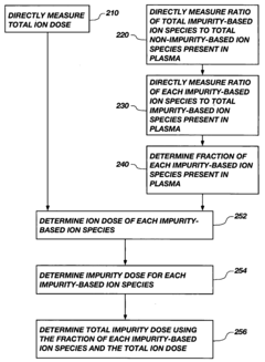
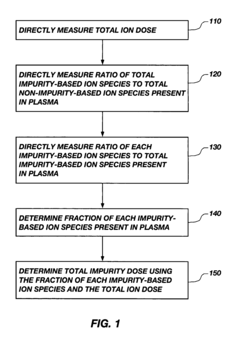
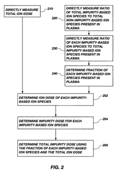
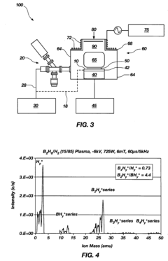
Innovation
- A method and apparatus that directly measure the total ion dose and plasma composition during the plasma doping process, using a Faraday cup and ion mass spectrometer to calculate the impurity dose in real-time without damaging the substrate, allowing for immediate adjustment of implant conditions.
Impurity introducing method, impurity introducing apparatus, and electronic device produced by using those
PatentWO2005031832A1
Innovation
- An impurity doping method that optically measures the physical properties of lattice defects in silicon substrates, allowing for precise control of annealing conditions and plasma composition to achieve efficient and accurate impurity introduction and activation without raising the substrate temperature.
Environmental Impact of Semiconductor Purification
The semiconductor purification process, while essential for achieving the high purity standards required in modern electronics, carries significant environmental implications that cannot be overlooked. Traditional purification methods often involve energy-intensive processes and hazardous chemicals, resulting in substantial carbon footprints and potential ecological risks. Recent studies indicate that semiconductor manufacturing facilities can consume between 2-5 million gallons of water daily, with purification processes accounting for approximately 40% of this consumption.
High-throughput experimentation (HTE) approaches to semiconductor purification are transforming this environmental landscape by enabling more efficient resource utilization. By simultaneously testing multiple purification parameters, HTE reduces the overall energy consumption by an estimated 30-45% compared to conventional sequential testing methods. This efficiency gain translates directly to reduced greenhouse gas emissions, with some advanced facilities reporting carbon footprint reductions of up to 2,500 metric tons annually through HTE implementation.
Waste generation presents another critical environmental concern in semiconductor purification. Conventional processes typically produce 5-7 kilograms of hazardous waste per square centimeter of processed wafer material. HTE methodologies have demonstrated potential to reduce this waste generation by 25-35% through optimization of chemical usage and more precise targeting of impurities. Additionally, the accelerated development of greener purification agents through HTE has led to the identification of several biodegradable alternatives to traditional solvents.
Water conservation represents perhaps the most significant environmental benefit of HTE in semiconductor purification. Advanced HTE systems incorporate closed-loop water recycling capabilities, achieving water reuse rates of 85-95% in purification processes. This dramatic improvement addresses one of the industry's most pressing sustainability challenges, particularly in water-stressed regions where semiconductor manufacturing clusters are increasingly located.
The environmental benefits of HTE extend beyond direct resource conservation. By enabling more rapid identification of optimal purification parameters, these techniques accelerate the development of inherently cleaner technologies. For instance, HTE has facilitated the discovery of room-temperature purification methods for certain semiconductor materials, eliminating the need for energy-intensive heating processes that traditionally consumed 1.2-1.8 MWh per production batch.
Regulatory frameworks worldwide are increasingly recognizing these environmental advantages, with several jurisdictions now offering expedited permitting processes for facilities implementing HTE-based purification systems. This regulatory support further accelerates the adoption of environmentally superior purification technologies, creating a positive feedback loop that continues to drive innovation toward more sustainable semiconductor manufacturing practices.
Supply Chain Resilience for High-Purity Materials
The semiconductor industry's reliance on high-purity materials creates significant vulnerabilities in global supply chains. Recent geopolitical tensions, trade restrictions, and the COVID-19 pandemic have exposed critical weaknesses in the procurement of ultra-pure materials essential for semiconductor manufacturing. With over 90% of high-purity gases and chemicals concentrated in specific geographic regions, disruptions can rapidly cascade through the entire semiconductor ecosystem.
Supply chain resilience for high-purity materials requires multi-faceted approaches to mitigate these risks. Diversification of supplier networks represents a primary strategy, with leading manufacturers now implementing "N+1" supplier policies to ensure alternative sourcing options. This approach necessitates qualification of multiple vendors against stringent purity standards, creating additional demand for high-throughput experimentation methodologies.
Regional manufacturing capabilities are being developed as another resilience measure. The CHIPS Act in the United States and similar initiatives in Europe aim to establish domestic production of high-purity precursors and materials. These efforts face significant challenges in replicating the specialized knowledge and infrastructure developed over decades in established manufacturing centers.
Inventory management strategies have evolved beyond traditional just-in-time approaches. Semiconductor manufacturers now maintain strategic reserves of critical high-purity materials, with some companies extending buffer stocks from typical 2-3 month supplies to 6-12 months for materials identified as high-risk. This shift requires enhanced storage capabilities that maintain material integrity over longer periods.
Advanced analytics and AI-driven supply chain monitoring systems provide early warning of potential disruptions. These systems integrate data from supplier operations, geopolitical developments, and transportation networks to predict supply chain vulnerabilities before they impact production. The effectiveness of these systems depends on accurate characterization of material purity and consistency across different suppliers.
Circular economy initiatives are emerging as long-term solutions for supply chain resilience. Reclamation and recycling of high-purity materials from manufacturing waste and end-of-life products can reduce dependence on primary sources. These approaches require sophisticated purification technologies to restore materials to semiconductor-grade standards, creating new opportunities for high-throughput experimentation in purification processes.
Standardization efforts across the industry aim to reduce qualification barriers when switching between suppliers. Organizations like SEMI and JEDEC are developing unified purity standards and testing protocols that would enable more flexible sourcing strategies while maintaining quality assurance. These standards must balance rigorous purity requirements with practical implementation across diverse global supply chains.
Unlock deeper insights with PatSnap Eureka Quick Research — get a full tech report to explore trends and direct your research. Try now!
Generate Your Research Report Instantly with AI Agent
Supercharge your innovation with PatSnap Eureka AI Agent Platform!