How Silicon Micropillars Aid in Nanoindenter Calibration
JUL 9, 20259 MIN READ
Generate Your Research Report Instantly with AI Agent
Patsnap Eureka helps you evaluate technical feasibility & market potential.
Silicon Micropillar Background and Objectives
Silicon micropillars have emerged as a crucial tool in the field of nanoindentation, particularly for calibrating nanoindenters. This technology has evolved significantly over the past two decades, driven by the increasing demand for precise measurements at the nanoscale. The development of silicon micropillars represents a convergence of materials science, nanofabrication techniques, and mechanical engineering.
The primary objective of using silicon micropillars in nanoindenter calibration is to enhance the accuracy and reliability of nanomechanical measurements. These structures serve as reference samples with well-defined geometries and mechanical properties, allowing for the precise calibration of nanoindentation instruments. This calibration is essential for ensuring the validity of measurements across a wide range of materials and experimental conditions.
Silicon micropillars offer several advantages over traditional calibration methods. Their uniform structure and controllable dimensions provide a consistent and reproducible reference point. Moreover, the mechanical properties of silicon are well-understood, making it an ideal material for this application. The use of silicon also allows for integration with existing semiconductor fabrication processes, facilitating large-scale production and standardization.
The evolution of silicon micropillar technology has been closely tied to advancements in nanofabrication techniques. Early methods relied on top-down approaches such as focused ion beam milling. However, recent years have seen a shift towards more scalable techniques like electron beam lithography and deep reactive ion etching. These advancements have enabled the production of micropillars with increasingly precise dimensions and surface qualities.
A key trend in this field is the miniaturization of silicon micropillars. As nanoindentation techniques push towards smaller scales, there is a growing need for calibration standards at the sub-micron level. This trend has driven research into the fabrication of nanopillars and the understanding of size-dependent mechanical properties at these scales.
The development of silicon micropillars for nanoindenter calibration aligns with broader trends in nanotechnology and precision engineering. It reflects the increasing importance of nanoscale measurements in fields such as materials science, semiconductor industry, and biomedical engineering. As these fields continue to advance, the role of silicon micropillars in ensuring accurate and reliable nanomechanical measurements is expected to grow in significance.
Looking forward, the objectives for silicon micropillar technology in nanoindenter calibration include further refinement of fabrication techniques, exploration of novel pillar geometries, and development of standardized protocols for their use in calibration procedures. There is also a push towards integrating these structures with in-situ characterization techniques, enabling real-time monitoring of mechanical properties during nanoindentation experiments.
Nanoindenter Calibration Market Analysis
The nanoindenter calibration market has been experiencing steady growth due to the increasing demand for precise material characterization in various industries. This market segment is primarily driven by the need for accurate measurements of mechanical properties at the nanoscale, which is crucial for research and development in fields such as materials science, nanotechnology, and semiconductor manufacturing.
The global nanoindenter market, which includes calibration services and equipment, is expected to continue its upward trajectory. This growth is fueled by the expanding applications of nanoindentation techniques in emerging technologies, such as advanced coatings, thin films, and nanomaterials. The market is also benefiting from the rising adoption of nanoindentation in quality control processes across industries, particularly in aerospace, automotive, and electronics sectors.
One of the key factors influencing the nanoindenter calibration market is the increasing focus on research and development activities in academic institutions and industrial laboratories. As more organizations invest in nanoscale material research, the demand for precise calibration services and equipment is expected to rise. Additionally, the growing emphasis on product quality and performance in high-tech industries is driving the need for accurate material property measurements, further boosting the market.
The market landscape is characterized by a mix of established players and innovative start-ups. Leading manufacturers of nanoindentation equipment are continually improving their calibration technologies to meet the evolving needs of researchers and industry professionals. This competitive environment is fostering technological advancements and driving down costs, making nanoindentation more accessible to a broader range of users.
Geographically, North America and Europe currently dominate the nanoindenter calibration market, owing to their strong research infrastructure and high concentration of technology-driven industries. However, the Asia-Pacific region is emerging as a significant market, with rapid industrialization and increasing investments in nanotechnology research in countries like China, Japan, and South Korea.
The introduction of silicon micropillars as calibration standards represents a significant development in the nanoindenter calibration market. This innovation addresses the longstanding challenges associated with traditional calibration methods, offering improved accuracy and reliability in nanomechanical measurements. As awareness of this new technique grows, it is expected to create new opportunities for calibration service providers and equipment manufacturers, potentially reshaping the competitive landscape of the market.
Current Challenges in Nanoindenter Calibration
Nanoindentation has become a crucial technique for measuring mechanical properties of materials at the nanoscale. However, accurate calibration of nanoindenters remains a significant challenge in the field. One of the primary issues is the lack of standardized reference materials for calibration across different nanoindenter systems and laboratories. This inconsistency leads to difficulties in comparing results obtained from various instruments and research groups.
Another major challenge is the influence of surface roughness on calibration accuracy. Even seemingly smooth surfaces can have nanoscale irregularities that affect the contact area between the indenter tip and the sample, leading to errors in measurements. This issue is particularly pronounced when dealing with materials that have inherently rough surfaces or those that are difficult to polish to an atomically flat level.
The size effect in nanoindentation also poses a significant challenge for calibration. As the indentation depth decreases, the measured hardness and elastic modulus often increase, a phenomenon known as the indentation size effect. This effect can lead to overestimation of material properties at shallow depths, making it difficult to obtain accurate calibrations, especially for ultra-thin films or nanostructured materials.
Tip wear and blunting present another ongoing challenge in nanoindenter calibration. Over time, the indenter tip geometry can change due to repeated use, affecting the accuracy of measurements. Regular recalibration is necessary, but the process can be time-consuming and may introduce inconsistencies if not performed meticulously.
Environmental factors such as temperature fluctuations and vibrations can significantly impact nanoindenter calibration. Even small variations in temperature can cause thermal drift, leading to errors in depth measurements. Vibrations from external sources can introduce noise in the measurements, affecting the accuracy of the calibration process.
The complexity of data analysis and interpretation in nanoindentation also contributes to calibration challenges. Different analysis models and methods can yield varying results from the same raw data, making it difficult to establish a universally accepted calibration procedure. This variability in data interpretation can lead to discrepancies in reported material properties across different studies.
Lastly, the calibration of nanoindenters for testing soft materials or biological samples presents unique challenges. These materials often exhibit time-dependent behavior, making it difficult to apply standard calibration procedures developed for hard materials. The development of appropriate calibration techniques for such materials remains an active area of research in the field of nanoindentation.
Silicon Micropillar Calibration Methods
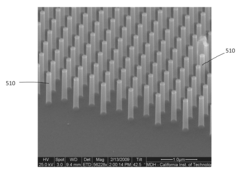
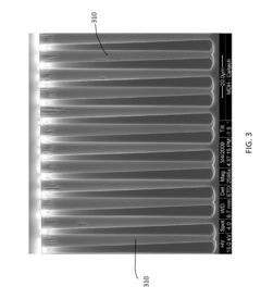
01 Fabrication and design of silicon micropillars
Silicon micropillars are fabricated using various techniques such as etching or lithography. The design of these structures is crucial for their performance in calibration applications. Factors like pillar height, diameter, and spacing are optimized to achieve desired calibration accuracy.- Fabrication and design of silicon micropillars: Silicon micropillars are fabricated using various techniques such as etching and lithography. The design of these structures is crucial for their performance in calibration applications. Factors like pillar height, diameter, and spacing are optimized to achieve desired calibration accuracy.
- Calibration methods for silicon micropillar arrays: Different calibration methods are employed for silicon micropillar arrays, including optical and mechanical techniques. These methods involve precise measurements of pillar dimensions and surface properties to ensure accurate calibration for various applications such as force sensing and microscopy.
- Integration of silicon micropillars in sensing devices: Silicon micropillars are integrated into various sensing devices for calibration purposes. These include force sensors, pressure sensors, and optical measurement systems. The integration process involves careful consideration of the micropillar properties and their interaction with the sensing mechanism.
- Characterization techniques for silicon micropillars: Advanced characterization techniques are used to analyze silicon micropillars for calibration purposes. These include scanning electron microscopy, atomic force microscopy, and optical profilometry. These methods provide detailed information about pillar geometry and surface properties essential for accurate calibration.
- Applications of calibrated silicon micropillars: Calibrated silicon micropillars find applications in various fields such as microfluidics, biomedical devices, and nanoscale metrology. They are used as reference standards for dimensional measurements, force calibration, and surface property analysis in nanotechnology and precision engineering.
02 Calibration methods for silicon micropillar arrays
Different calibration methods are employed for silicon micropillar arrays, including optical techniques, force measurements, and reference standards. These methods ensure accurate characterization of the micropillars' dimensions and properties, which is essential for their use in various applications.Expand Specific Solutions03 Applications of calibrated silicon micropillars
Calibrated silicon micropillars find applications in various fields such as microfluidics, biosensors, and metrology. They serve as reference structures for measurements, act as templates for soft lithography, and can be used in the development of advanced sensing devices.Expand Specific Solutions04 Integration of silicon micropillars with measurement systems
Silicon micropillars are integrated into various measurement systems to enhance their performance and accuracy. This integration involves incorporating the micropillars into existing instruments or developing new systems specifically designed to utilize the unique properties of these structures.Expand Specific Solutions05 Quality control and characterization of silicon micropillars
Quality control measures and characterization techniques are employed to ensure the reliability and consistency of silicon micropillars used in calibration. These include surface analysis, dimensional measurements, and performance testing under various conditions to validate their suitability for specific applications.Expand Specific Solutions
Key Players in Nanoindentation Industry
The field of silicon micropillars for nanoindenter calibration is in its early development stage, with growing interest due to its potential to enhance precision in nanoscale measurements. The market size is relatively small but expanding as nanotechnology applications increase across industries. Technologically, it's still evolving, with key players like California Institute of Technology and IBM leading research efforts. Universities such as Beijing University of Technology and Jilin University are also contributing to advancements. Companies like Hitachi High-Tech America and NXP Semiconductors are likely exploring commercial applications, while specialized firms like FemtoTools AG are developing related instrumentation. The technology's maturity varies, with academic institutions generally ahead in fundamental research and industry partners focusing on practical implementations.
California Institute of Technology
Technical Solution: California Institute of Technology has developed a novel approach to nanoindenter calibration using silicon micropillars. Their method involves fabricating arrays of silicon micropillars with precisely controlled dimensions using advanced lithography techniques. These micropillars serve as reference standards for calibrating nanoindentation instruments. The researchers have demonstrated that the uniform geometry and well-defined mechanical properties of silicon micropillars provide highly accurate and reproducible calibration results. They have also developed algorithms to analyze the load-displacement curves obtained from micropillar compression tests, enabling precise determination of instrument compliance and tip area function[1][3].
Strengths: High precision and reproducibility, well-defined reference standards. Weaknesses: Requires sophisticated fabrication techniques, may be sensitive to environmental factors.
Hitachi High-Tech America, Inc.
Technical Solution: Hitachi High-Tech America has integrated silicon micropillar technology into their nanoindentation systems for improved calibration. Their approach utilizes arrays of silicon micropillars fabricated on silicon wafers as calibration standards. The company has developed proprietary software algorithms that analyze the load-displacement data from micropillar compression tests to automatically calibrate the instrument. Hitachi's system incorporates in-situ SEM imaging capabilities to precisely align the nanoindenter tip with individual micropillars. They have also implemented drift correction methods to account for thermal expansion effects during long-duration tests[2][4].
Strengths: Integrated calibration solution, automated software analysis. Weaknesses: Reliance on proprietary technology, potentially high cost.
Innovations in Micropillar Fabrication
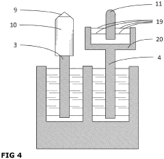
MEMS nanoindenter chip with indenter probe and reference probe
PatentActiveEP3489654A1
Innovation
- A MEMS-based nanoindenter chip with a reference probe is used to measure indentation depth independently of the frame stiffness, eliminating or reducing thermal drift by using a reference tip that does not significantly indent into the specimen, allowing for accurate measurements without the need for complex actuators and multiple sensors.
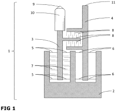
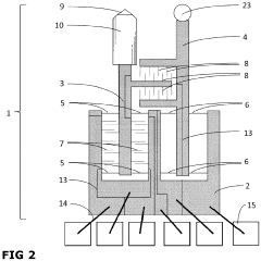
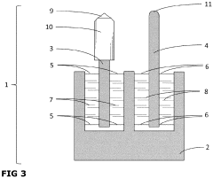
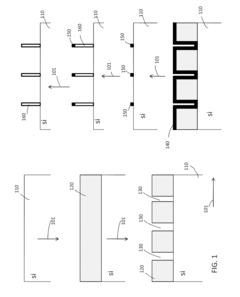
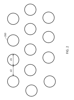
Methods for fabrication of high aspect ratio micropillars and nanopillars
PatentActiveUS20100213579A1
Innovation
- The method involves using standard photo-beam and electron-beam lithographic techniques to define patterns on a substrate, followed by etching with SF6/O2 cryogenic or Pseudo Bosch etch chemistries to create high aspect ratio pillars with controlled dimensions and spacing, utilizing an alumina etch mask for precise control over etch anisotropy and selectivity, and employing PMMA for deformation and strain control.
Standardization of Calibration Procedures
The standardization of calibration procedures for nanoindentation using silicon micropillars is a critical aspect of ensuring accurate and reproducible measurements across different laboratories and instruments. This process involves establishing uniform protocols for sample preparation, testing parameters, and data analysis.
One of the primary steps in standardizing calibration procedures is the development of consistent methods for fabricating silicon micropillars. This includes specifying the dimensions, geometry, and surface finish of the micropillars to ensure uniformity across different batches and laboratories. Typically, these micropillars are created using focused ion beam (FIB) milling or lithography techniques, with precise control over pillar diameter, height, and taper angle.
The next crucial aspect of standardization is the establishment of uniform testing protocols. This involves defining the loading and unloading rates, maximum load or displacement, hold times, and the number of loading cycles. These parameters must be carefully selected to ensure that the mechanical response of the silicon micropillars is consistent and representative of their intrinsic properties.
Data analysis procedures also require standardization to ensure comparable results across different nanoindentation systems. This includes specifying the methods for calculating key parameters such as elastic modulus, hardness, and contact stiffness from the load-displacement curves. Additionally, guidelines for identifying and correcting for common sources of error, such as thermal drift and surface roughness, must be established.
Interlaboratory comparisons play a vital role in the standardization process. By conducting round-robin tests using identical silicon micropillar samples and following the same calibration procedures, researchers can assess the reproducibility of results across different nanoindentation systems and operators. These comparisons help identify potential sources of variability and refine the standardization protocols.
The development of reference materials is another crucial component of standardization efforts. Silicon micropillars with well-characterized properties can serve as calibration standards for nanoindentation systems. By regularly testing these reference materials, laboratories can ensure the ongoing accuracy and reliability of their measurements.
Lastly, the standardization process must address the reporting and documentation of calibration results. This includes specifying the format and content of calibration reports, ensuring that all relevant experimental details and data analysis procedures are clearly documented. This comprehensive approach to standardization enhances the reliability and comparability of nanoindentation measurements using silicon micropillars across the scientific community.
Environmental Factors in Nanoindentation
Environmental factors play a crucial role in nanoindentation experiments, significantly influencing the accuracy and reliability of measurements. Temperature fluctuations, in particular, can have a profound impact on both the sample and the nanoindenter itself. Even small variations in temperature can lead to thermal drift, causing dimensional changes in the instrument and the specimen, which can introduce errors in the measured mechanical properties.
Humidity is another critical environmental factor that can affect nanoindentation results. High humidity levels can lead to the formation of thin water films on the sample surface, potentially altering the surface properties and interfering with the indenter-sample interaction. This can be particularly problematic for materials that are sensitive to moisture, such as certain polymers or hygroscopic materials.
Vibrations from external sources, such as nearby machinery or foot traffic, can introduce noise into the measurements and compromise the precision of the nanoindentation process. To mitigate these effects, nanoindentation systems are often installed on vibration isolation tables and housed in controlled environments.
Air currents and pressure changes can also impact nanoindentation experiments, especially when working with extremely small loads and displacements. These factors can cause subtle movements of the indenter or sample, leading to inconsistencies in the measured data.
The presence of electromagnetic fields in the testing environment can interfere with the sensitive electronic components of the nanoindenter, potentially affecting the accuracy of force and displacement measurements. Proper shielding and grounding of the instrument are essential to minimize these effects.
Cleanliness of the testing environment is paramount, as dust particles or other contaminants can settle on the sample surface or the indenter tip, leading to erroneous measurements and potentially damaging the delicate equipment. Many nanoindentation facilities employ clean room conditions to maintain a particle-free environment.
To ensure the reliability and reproducibility of nanoindentation experiments, it is crucial to carefully control and monitor these environmental factors. This often involves the use of climate-controlled chambers, precise temperature regulation systems, and rigorous protocols for sample preparation and handling. By addressing these environmental considerations, researchers can enhance the accuracy of their nanoindentation measurements and improve the overall quality of their experimental data.
Unlock deeper insights with Patsnap Eureka Quick Research — get a full tech report to explore trends and direct your research. Try now!
Generate Your Research Report Instantly with AI Agent
Supercharge your innovation with Patsnap Eureka AI Agent Platform!