

How to Enhance Hall Effect Sensor Resolution for Precision Tasks
SEP 22, 202510 MIN READ
Generate Your Research Report Instantly with AI Agent
PatSnap Eureka helps you evaluate technical feasibility & market potential.
Hall Effect Sensor Technology Background and Objectives
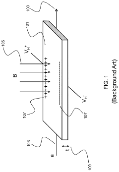
Hall Effect sensors, discovered by Edwin Hall in 1879, have evolved from simple magnetic field detectors to sophisticated precision instruments critical in modern industrial and consumer applications. The fundamental principle remains unchanged: when a current-carrying conductor is placed in a magnetic field, a voltage is generated perpendicular to both the current and magnetic field. This Hall voltage is proportional to the magnetic field strength, enabling measurement of magnetic fields, position, rotation, and current.
The evolution of Hall Effect sensor technology has been marked by significant advancements in materials science, semiconductor fabrication, and signal processing. Early sensors offered limited resolution and were primarily used in simple on/off applications. The introduction of integrated circuits in the 1970s enabled the integration of amplification and signal conditioning circuits directly with the sensing element, dramatically improving performance and reliability.
Recent decades have witnessed exponential growth in precision applications requiring high-resolution magnetic field measurements. Industries such as automotive, aerospace, medical devices, and industrial automation increasingly demand sensors capable of detecting minute changes in magnetic fields with exceptional accuracy. This trend has driven the development of enhanced Hall Effect sensors with resolutions approaching the micro-gauss range.
The current technological landscape presents both opportunities and challenges. While traditional Hall Effect sensors typically achieve resolutions in the 10-100 gauss range, precision tasks in fields like robotics, medical diagnostics, and scientific instrumentation require resolutions orders of magnitude higher. This gap represents a critical area for technological advancement and innovation.
The primary objective of enhancing Hall Effect sensor resolution is to enable new applications in precision measurement and control systems. Specifically, the goals include achieving sub-gauss resolution while maintaining stability across varying environmental conditions, reducing noise susceptibility, minimizing power consumption, and ensuring cost-effectiveness for mass production.
Technical objectives also encompass improving temperature stability, as Hall Effect sensors traditionally suffer from significant temperature drift that limits their precision in variable environments. Additionally, there is a push toward miniaturization without compromising performance, enabling integration into increasingly compact devices and systems.
The convergence of advanced materials research, microfabrication techniques, and sophisticated signal processing algorithms presents promising pathways for resolution enhancement. Emerging technologies such as quantum Hall effect sensors and graphene-based Hall devices represent frontier research areas with potential for breakthrough improvements in resolution capabilities.
As industries continue to demand higher precision in sensing technologies, the evolution of Hall Effect sensors toward higher resolution represents not just a technical challenge but a significant market opportunity. The trajectory of development points toward integrated smart sensor systems combining high-resolution Hall Effect elements with advanced processing capabilities, enabling self-calibration and adaptive performance optimization.
Market Demand Analysis for High-Resolution Position Sensing
The global market for high-resolution position sensing technologies has experienced significant growth in recent years, driven primarily by increasing automation across multiple industries. The demand for Hall Effect sensors with enhanced resolution capabilities is particularly pronounced in precision manufacturing, automotive systems, robotics, and medical devices where accurate position detection is critical for operational success.
In the industrial automation sector, the need for high-precision position sensing has grown at approximately 8% annually since 2019, with manufacturers seeking sensors capable of sub-micron resolution for advanced manufacturing processes. This demand is particularly evident in semiconductor fabrication equipment, where positioning accuracy directly impacts product quality and yield rates.
The automotive industry represents another substantial market segment, with modern vehicles containing an average of 15-25 position sensors per vehicle. The transition toward electric and autonomous vehicles has intensified the need for high-resolution sensing technologies, as these advanced systems require more precise control mechanisms than traditional combustion engine vehicles.
Medical technology applications constitute a rapidly expanding market for high-resolution position sensing, particularly in surgical robotics and imaging equipment. The market size for medical robotics alone reached $5.9 billion in 2022, with position sensing components representing a critical enabling technology within these systems.
Consumer electronics manufacturers are increasingly incorporating position sensing technologies in next-generation devices, creating new market opportunities for miniaturized, high-resolution Hall Effect sensors. This trend is evident in the growing adoption of gesture control interfaces and precision haptic feedback systems in smartphones, wearables, and gaming devices.
Market research indicates that customers across these sectors prioritize several key performance attributes when selecting position sensing solutions: measurement resolution, temperature stability, power consumption, form factor, and cost-effectiveness. The demand for sensors that can maintain high resolution across varying environmental conditions has become particularly important as applications expand into more challenging operational environments.
Regional analysis shows that Asia-Pacific currently leads in market volume, driven by the region's dominant position in electronics manufacturing, while North America leads in high-value applications requiring the most advanced sensing capabilities. Europe shows strong demand in automotive and industrial automation segments, with particular emphasis on sensors meeting stringent reliability and safety standards.
The overall market trajectory suggests continued growth at a compound annual rate of 6.5% through 2028, with the highest growth rates expected in emerging applications such as collaborative robotics, advanced driver assistance systems, and next-generation medical devices where positioning accuracy directly correlates with system performance and safety.
Current Limitations and Technical Challenges in Hall Sensors
Despite significant advancements in Hall effect sensor technology, several critical limitations continue to impede their application in high-precision tasks. The fundamental challenge lies in the inherently low signal-to-noise ratio (SNR) of Hall sensors, particularly when measuring weak magnetic fields. This limitation stems from the relatively small Hall voltage generated in conventional semiconductor materials, which typically ranges from microvolts to millivolts, making it susceptible to various noise sources.
Temperature dependency represents another significant obstacle, as Hall sensor sensitivity can drift by 0.1% to 0.5% per degree Celsius without proper compensation. This thermal drift introduces substantial measurement errors in environments with fluctuating temperatures, severely limiting precision in industrial applications and automotive systems where temperature variations are common.
Nonlinearity issues further compromise measurement accuracy, with most commercial Hall sensors exhibiting nonlinearity errors of 0.5% to 2% across their full measurement range. This nonlinearity becomes particularly problematic when precise measurements are required across a wide dynamic range, such as in position sensing for robotics or advanced manufacturing equipment.
Offset voltage presents an additional challenge, as even in the absence of a magnetic field, Hall sensors produce a non-zero output voltage. This offset can vary between individual sensors and drift over time due to aging effects and environmental factors, necessitating complex calibration procedures that increase system complexity and cost.
Material limitations also constrain performance, as traditional silicon-based Hall sensors suffer from relatively low carrier mobility, limiting their sensitivity. While alternative materials like gallium arsenide (GaAs) and indium antimonide (InSb) offer improved sensitivity, they introduce manufacturing complexities and higher costs that restrict widespread adoption.
Integration challenges persist when incorporating high-resolution Hall sensors into miniaturized systems. The need for signal conditioning circuits, temperature compensation, and noise filtering components increases the overall footprint and power consumption, creating design trade-offs in space-constrained applications like wearable devices and medical implants.
Cross-axis sensitivity represents another significant technical hurdle, where Hall sensors respond to magnetic fields perpendicular to their intended sensing axis. This cross-sensitivity, typically ranging from 1% to 5% of the primary axis sensitivity, introduces measurement errors in applications requiring precise directional magnetic field detection, such as 3D position tracking and navigation systems.
Current High-Resolution Hall Sensor Solutions
01 Design factors affecting Hall sensor resolution
The resolution of Hall effect sensors is influenced by various design factors including the semiconductor material used, the geometry of the sensing element, and the integration with signal processing circuits. Optimizing these design elements can significantly improve the sensor's ability to detect small magnetic field changes, thereby enhancing resolution. Advanced semiconductor materials and precise fabrication techniques allow for more sensitive Hall elements that can detect smaller magnetic field variations.- Enhancing Hall sensor resolution through design optimization: Hall effect sensor resolution can be improved through various design optimizations including geometric modifications, material selection, and structural enhancements. These optimizations focus on increasing the sensitivity of the sensor to magnetic field changes while reducing noise. Advanced semiconductor materials and specialized fabrication techniques can significantly improve the sensor's ability to detect smaller magnetic field variations, thereby enhancing overall resolution.
- Signal processing techniques for improved resolution: Various signal processing techniques can be employed to enhance the resolution of Hall effect sensors. These include amplification circuits, filtering algorithms, and digital signal processing methods that can extract meaningful data from weak Hall voltage signals. Advanced processing techniques help in noise reduction, offset compensation, and can implement dynamic range adjustment to improve the sensor's ability to detect small magnetic field changes accurately.
- Multi-axis and integrated Hall sensor systems: Multi-axis Hall effect sensor systems can provide enhanced resolution by measuring magnetic fields in multiple directions simultaneously. These integrated systems often combine multiple sensing elements with specialized circuitry to provide comprehensive magnetic field measurement. The integration of multiple sensors allows for better spatial resolution and can compensate for cross-axis interference, resulting in more accurate and higher resolution magnetic field measurements.
- Temperature compensation and calibration methods: Temperature variations can significantly affect Hall sensor resolution. Advanced temperature compensation techniques and calibration methods are employed to maintain high resolution across a wide temperature range. These methods include integrated temperature sensors, compensation circuits, and algorithmic approaches that adjust sensor output based on temperature readings. Proper calibration procedures during manufacturing and in-field operation ensure consistent resolution performance under varying environmental conditions.
- Miniaturization and packaging innovations: Advancements in miniaturization and packaging technologies have led to improved Hall sensor resolution. Smaller sensing elements can detect more localized magnetic fields, while innovative packaging solutions reduce interference and noise. These innovations include specialized shielding techniques, optimized placement of sensing elements, and advanced packaging materials that protect the sensor while maintaining its sensitivity. Miniaturized Hall sensors can achieve higher spatial resolution while consuming less power.
02 Signal processing techniques for improved resolution
Various signal processing techniques can be employed to enhance the resolution of Hall effect sensors. These include amplification, filtering, and digital signal processing methods that reduce noise and increase the signal-to-noise ratio. Advanced algorithms can compensate for temperature drift and other environmental factors that might affect measurement accuracy. Implementing these techniques allows Hall sensors to achieve higher resolution measurements even in challenging environments.Expand Specific Solutions03 Integrated circuit implementations for high-resolution sensing
Integrating Hall effect sensors with specialized circuitry on a single chip can significantly improve resolution capabilities. These integrated solutions often incorporate temperature compensation, offset cancellation, and chopper stabilization techniques. By combining the sensing element with dedicated processing circuits, manufacturers can achieve higher resolution while minimizing size and power consumption. These integrated approaches also help standardize performance across different operating conditions.Expand Specific Solutions04 Differential and array-based Hall sensor configurations
Differential Hall sensor configurations and sensor arrays can be used to enhance resolution by canceling common-mode noise and improving signal detection. By using multiple sensing elements in specific arrangements, these configurations can detect smaller magnetic field variations and provide more precise measurements. Array-based approaches also enable spatial mapping of magnetic fields at higher resolutions than single-element sensors, making them suitable for applications requiring detailed magnetic field analysis.Expand Specific Solutions05 Calibration and compensation methods for resolution enhancement
Various calibration and compensation methods can be applied to Hall effect sensors to enhance their resolution. These include techniques for offset voltage compensation, temperature drift correction, and non-linearity adjustment. Factory calibration procedures and self-calibration capabilities built into sensor systems can significantly improve measurement accuracy and resolution. These methods often involve storing calibration parameters in memory and applying corrections during operation to achieve optimal performance across varying conditions.Expand Specific Solutions
Key Industry Players and Competitive Landscape
The Hall Effect sensor resolution enhancement market is currently in a growth phase, with increasing demand for precision applications driving innovation. The market is expanding rapidly due to adoption in automotive, industrial automation, and consumer electronics sectors, with an estimated global value exceeding $2 billion. Leading players like STMicroelectronics, Texas Instruments, and Infineon Technologies are advancing sensor technology through integrated circuit solutions that improve signal-to-noise ratios and digital processing capabilities. Honeywell and Bosch have established strong positions in industrial and automotive applications, while emerging players such as ams-OSRAM and Asahi Kasei Microdevices are focusing on miniaturization and power efficiency. Research institutions including CEA and Tokyo Institute of Technology are collaborating with industry leaders to develop next-generation sensing technologies incorporating quantum effects and novel materials to push resolution boundaries.
STMicroelectronics International NV
Technical Solution: STMicroelectronics has developed the MLX90xxx series of high-precision Hall effect sensors utilizing their proprietary IMC (Integrated Magneto-Concentrator) technology, which significantly enhances magnetic field sensitivity without compromising stability. This approach integrates ferromagnetic flux concentrators directly onto the silicon die, amplifying the magnetic field at the sensing element by factors of 5-10x[2]. Their sensors implement advanced chopper stabilization techniques operating at frequencies above 150kHz to minimize low-frequency noise components that typically limit resolution. ST's approach incorporates on-chip temperature sensors with real-time compensation algorithms that adjust gain and offset parameters across the full operating temperature range (-40°C to +150°C). For precision applications, they've developed sensors with integrated 24-bit sigma-delta ADCs that oversample the Hall voltage at rates up to 200kHz, then apply digital filtering to achieve effective resolutions exceeding 16 bits[4]. Their latest generation implements a multi-Hall element architecture where multiple sensing elements are arranged in optimized geometric patterns and their outputs are combined using proprietary algorithms to cancel systematic errors and enhance signal-to-noise ratio by up to 6dB compared to single-element designs.
Strengths: Exceptional sensitivity (down to 1mV/G) enables detection of very small magnetic field changes, ideal for precision positioning tasks. Their highly integrated approach minimizes external component requirements. Weaknesses: The advanced signal processing introduces latency that may limit suitability for high-speed control applications, and the sensors require careful calibration to achieve specified performance.
Texas Instruments Incorporated
Technical Solution: Texas Instruments has pioneered high-resolution Hall effect sensing through their DRV5000 series, which incorporates BiCMOS technology to combine high-performance analog front-end with digital processing capabilities. Their approach utilizes chopper stabilization techniques operating at frequencies above 200kHz to minimize 1/f noise, a critical factor limiting resolution in conventional Hall sensors[2]. TI's sensors employ spinning current techniques that systematically eliminate offset errors by rotating the bias current through the Hall element and averaging multiple measurements. Their latest generation incorporates on-chip 16-bit sigma-delta ADCs with programmable oversampling ratios, allowing trade-offs between resolution and response time based on application requirements. For precision motion control applications, TI has developed sensors with integrated angle calculation algorithms that can achieve angular resolution below 0.1 degrees when used in rotary position sensing configurations[4]. The company's DRV5053 devices feature programmable gain amplifiers that can be dynamically adjusted to optimize the sensing range for specific operating conditions.
Strengths: Excellent noise performance (down to 8μV/√Hz) and high integration level reducing system complexity. Their programmable architecture allows customization for specific applications. Weaknesses: Higher power consumption compared to simpler Hall sensors and more complex configuration requirements that may increase implementation time.
Core Patents and Innovations in Hall Effect Technology
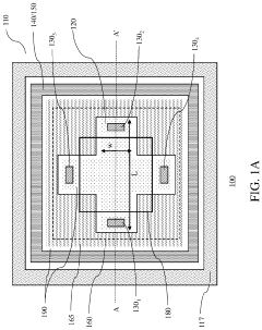
Hall effect sensor with enhanced sensitivity and method for producing the same
PatentActiveUS10707408B2
Innovation
- A Hall effect sensor is formed with a thin Hall plate and optional front and back gates, and reduced or omitted doping to enhance sensitivity, using a silicon-on-insulator (SOI) substrate with shallow trench isolation (STI) structures and N+ dopant ion implantation to create N+ implantation regions.
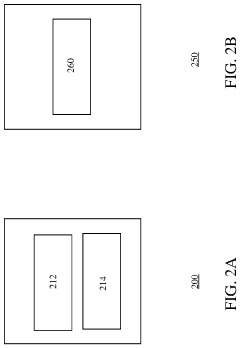
Hall effect sensors with tunable sensitivity and/or resistance
PatentActiveUS11047930B2
Innovation
- A Hall effect sensor design with a tunable Hall plate thickness, achieved through adjustable implants in the separation layer and bias voltage applied to the separation layer, allowing for customizable current sensitivity and resistance, enabling high voltage and current sensitivity in the same device.
Material Science Advancements for Hall Sensor Performance
Material science innovations have become a cornerstone in advancing Hall effect sensor technology, particularly for high-precision applications. Recent developments in semiconductor materials have significantly enhanced sensor sensitivity and resolution capabilities. Traditional silicon-based Hall sensors are increasingly being supplemented or replaced by compound semiconductors such as gallium arsenide (GaAs) and indium antimonide (InSb), which demonstrate superior electron mobility characteristics—up to 20 times higher than conventional silicon.
The emergence of graphene as a two-dimensional material has revolutionized Hall sensor design. With its exceptional carrier mobility exceeding 200,000 cm²/Vs at room temperature, graphene-based Hall sensors can detect magnetic fields in the nano-Tesla range, representing a substantial improvement over traditional materials. This breakthrough enables applications in biomagnetic field detection and quantum computing where ultra-high precision is paramount.
Heterostructure engineering has also contributed significantly to Hall sensor advancement. By creating precisely controlled layers of different semiconductor materials, researchers have developed quantum well structures that confine electrons in two dimensions, dramatically increasing the Hall coefficient and improving signal-to-noise ratios. These quantum well Hall sensors exhibit enhanced temperature stability and reduced drift, critical factors for industrial precision measurement systems.
Nanomaterial integration represents another frontier in Hall sensor development. Magnetic nanoparticles incorporated into sensing elements can amplify the local magnetic field, effectively boosting sensor sensitivity without requiring additional power consumption. This approach has yielded promising results in automotive position sensing applications, where sub-micron precision is increasingly demanded for advanced driver assistance systems.
Thin-film deposition techniques have evolved to enable atomic-level precision in material layering, crucial for creating high-performance Hall sensors. Advanced methods such as atomic layer deposition (ALD) and molecular beam epitaxy (MBE) allow for unprecedented control over material composition and interface quality, reducing carrier scattering and improving overall sensor performance. These techniques have facilitated the development of Hall sensors with resolution improvements of up to 300% compared to conventionally manufactured devices.
The incorporation of rare earth materials as dopants has emerged as another promising direction. Elements such as neodymium and samarium can enhance magnetic field interaction within semiconductor materials, increasing the Hall voltage output for a given field strength. This approach has proven particularly effective in extreme environment applications where traditional sensors would suffer from performance degradation.
Integration Strategies with Signal Processing Systems
Effective integration of Hall Effect sensors with signal processing systems represents a critical pathway to achieving enhanced resolution for precision applications. Modern signal processing architectures can extract maximum performance from these sensors through strategic implementation of both hardware and software solutions. The integration typically begins at the analog front-end, where precision instrumentation amplifiers with low noise characteristics and high common-mode rejection ratios form the first critical interface with the sensor output.
Digital signal processors (DSPs) or field-programmable gate arrays (FPGAs) serve as the computational backbone of advanced Hall sensor systems, enabling real-time filtering and signal enhancement. These platforms support sophisticated algorithms including adaptive filtering, which dynamically adjusts to changing environmental conditions, and oversampling techniques that can effectively increase resolution beyond the native capabilities of the sensor hardware.
Implementation of delta-sigma modulation represents another valuable integration strategy, converting analog signals to high-resolution digital outputs while inherently providing noise shaping benefits. This approach pushes quantization noise to higher frequencies where it can be more easily filtered, resulting in cleaner signals in the frequency band of interest.
For systems requiring maximum precision, closed-loop feedback architectures can be implemented where the processed Hall sensor output drives compensation mechanisms that actively stabilize the measurement environment. This approach is particularly valuable in applications where external magnetic field variations or temperature fluctuations might otherwise compromise measurement accuracy.
Embedded calibration routines represent another critical integration element, allowing systems to periodically self-calibrate against known reference points. These routines can compensate for drift characteristics that develop over time or with changing environmental conditions, maintaining high resolution performance throughout the operational lifetime of the sensor system.
Network connectivity features enable distributed sensor arrays to function as coordinated measurement systems, with centralized signal processing resources handling data from multiple Hall sensors simultaneously. This approach facilitates spatial averaging and differential measurement techniques that can substantially improve overall system resolution beyond what individual sensors might achieve in isolation.
The most advanced integration strategies incorporate machine learning algorithms that can identify and compensate for systematic error patterns in sensor outputs. These systems effectively "learn" the unique characteristics and limitations of specific sensor implementations, applying customized correction factors that optimize performance for particular application requirements and environmental conditions.
Unlock deeper insights with PatSnap Eureka Quick Research — get a full tech report to explore trends and direct your research. Try now!
Generate Your Research Report Instantly with AI Agent
Supercharge your innovation with PatSnap Eureka AI Agent Platform!