How to Enhance Spin Injection Efficiency Using Novel Contact Materials
AUG 27, 20259 MIN READ
Generate Your Research Report Instantly with AI Agent
Patsnap Eureka helps you evaluate technical feasibility & market potential.
Spin Injection Technology Background and Objectives
Spin injection technology has evolved significantly over the past two decades, emerging as a cornerstone of spintronics—a field that leverages electron spin for information processing and storage. The fundamental concept dates back to the 1980s when scientists first proposed utilizing spin-polarized currents for electronic applications. However, practical implementations gained momentum only in the early 2000s with breakthroughs in materials science and nanofabrication techniques.
The evolution trajectory shows a clear shift from theoretical frameworks to experimental validations, with significant milestones including the demonstration of spin injection across various interfaces, particularly metal-semiconductor and ferromagnet-nonmagnet junctions. Recent advancements have focused on overcoming the conductivity mismatch problem, which has been a persistent challenge limiting spin injection efficiency in practical devices.
Current research trends indicate growing interest in novel contact materials beyond traditional ferromagnetic metals, including half-metallic ferromagnets, topological insulators, and two-dimensional materials. These materials offer unique band structures and spin-orbit coupling properties that potentially enable more efficient spin polarization and transport across interfaces.
The primary technical objective in this field is to achieve near-unity spin injection efficiency at room temperature in practical device configurations. This involves developing contact materials and interface engineering techniques that minimize spin scattering, prevent depolarization, and ensure efficient spin transport across heterojunctions.
Secondary objectives include enhancing spin coherence length, reducing energy consumption during the injection process, and ensuring compatibility with existing semiconductor fabrication technologies for seamless integration into commercial electronic devices.
From a broader perspective, efficient spin injection represents a critical enabling technology for next-generation computing paradigms, including spin-based logic, non-volatile magnetic memory, and quantum computing. The ability to reliably inject and detect spin-polarized currents forms the foundation upon which these advanced applications can be built.
The technical roadmap for spin injection technology anticipates several key developments, including the standardization of measurement techniques for accurately quantifying spin injection efficiency, the establishment of theoretical frameworks that better predict material combinations for optimal performance, and the development of scalable fabrication methods for novel contact materials that maintain their spin-selective properties at nanoscale dimensions.
Market Analysis for Spintronics Applications
The global spintronics market is experiencing robust growth, projected to reach $12.8 billion by 2027, with a compound annual growth rate of 34.8% from 2021. This accelerated expansion is primarily driven by increasing demand for energy-efficient data storage solutions and the growing adoption of spintronics-based sensors across multiple industries.
The market segmentation reveals distinct application categories where enhanced spin injection efficiency would create immediate value. Data storage applications currently dominate the market share at approximately 42%, with magnetic random-access memory (MRAM) emerging as the fastest-growing segment due to its non-volatility, high speed, and low power consumption advantages. The development of novel contact materials that improve spin injection efficiency could potentially double MRAM performance metrics, creating a significant competitive advantage.
Sensor applications represent the second-largest market segment at 28%, with automotive and industrial sectors showing particularly strong demand growth. Improved spin injection efficiency would enable higher sensitivity magnetoresistive sensors, expanding their application range in autonomous vehicles, industrial automation, and IoT devices. Market analysis indicates that a 30% improvement in spin injection efficiency could unlock an additional $1.5 billion market opportunity in these sectors by 2025.
Geographically, North America currently leads the spintronics market with 38% share, followed by Asia-Pacific at 34% and Europe at 22%. However, the Asia-Pacific region is demonstrating the highest growth rate, driven by substantial investments in semiconductor manufacturing infrastructure and research initiatives in China, South Korea, and Japan. These regional dynamics create differentiated market entry opportunities for novel contact material technologies.
From an industry perspective, key stakeholders include semiconductor manufacturers, electronic device producers, and automotive companies. Consumer electronics represents 36% of end-user applications, followed by automotive (24%), healthcare (18%), and industrial automation (14%). The healthcare segment is projected to grow at the highest rate due to emerging applications in medical imaging and biosensing that would benefit significantly from enhanced spin injection efficiency.
Market barriers include high initial implementation costs, technical complexity, and competition from established technologies. However, customer surveys indicate willingness to adopt spintronics solutions that demonstrate clear performance advantages and energy efficiency improvements of at least 25% over conventional electronics – a threshold that novel contact materials could potentially achieve.
Current Challenges in Spin Injection Efficiency
Spin injection efficiency remains a critical bottleneck in spintronic device development, with current technologies struggling to achieve the high efficiency levels required for practical applications. The fundamental challenge lies in the conductivity mismatch between ferromagnetic materials and semiconductors, which causes significant spin polarization loss at the interface. This mismatch creates a barrier that filters out spin-polarized electrons, resulting in dramatically reduced spin injection rates that often fall below 1% efficiency in conventional metal-semiconductor junctions.
Material interface quality presents another substantial hurdle, as atomic-level imperfections, interdiffusion, and chemical reactions at contact points create scattering centers that randomize spin orientation. Even minor interface contamination can disrupt the spin coherence length, severely degrading device performance. Additionally, the formation of Schottky barriers at metal-semiconductor interfaces further complicates spin transport by creating depletion regions that impede efficient carrier movement.
Temperature stability poses significant challenges, with many promising materials exhibiting excellent spin injection properties only at extremely low temperatures. As operating temperatures increase toward room temperature, thermal fluctuations induce spin relaxation and decoherence, dramatically reducing injection efficiency. This temperature dependence severely limits practical applications in consumer electronics and industrial settings where ambient temperature operation is essential.
Current fabrication techniques introduce additional complications through process-induced defects and limitations in precise interface control. Conventional deposition methods often create unintended oxidation layers or structural defects that act as spin-flipping centers. The inability to consistently produce atomically clean interfaces at scale represents a major manufacturing challenge that hampers commercialization efforts.
Spin relaxation mechanisms, including Elliott-Yafet and D'yakonov-Perel processes, further reduce efficiency by causing spin depolarization during transport. These intrinsic mechanisms become particularly problematic in materials with strong spin-orbit coupling or in devices requiring longer spin transport distances. The characteristic spin diffusion length in most materials remains too short for practical device dimensions, necessitating either extremely miniaturized components or novel materials with enhanced spin preservation properties.
Measurement and characterization difficulties compound these technical challenges, as accurately quantifying spin injection efficiency requires sophisticated techniques like Hanle effect measurements or spin-resolved spectroscopy. The lack of standardized measurement protocols creates inconsistencies in reported values across research groups, making objective comparison of different contact materials and approaches problematic for systematic advancement of the field.
State-of-the-Art Contact Materials and Interfaces
01 Ferromagnetic materials for spin injection
Ferromagnetic materials are used as contact materials for efficient spin injection in spintronic devices. These materials, which have inherent magnetic properties, can generate spin-polarized currents when in contact with semiconductors or other materials. The efficiency of spin injection depends on the interface quality between the ferromagnetic material and the non-magnetic layer. Various ferromagnetic metals and alloys have been developed to optimize spin polarization and reduce conductivity mismatch issues.- Ferromagnetic materials for spin injection: Ferromagnetic materials are used as contact materials for spin injection in spintronic devices. These materials have inherent magnetic properties that allow for efficient spin polarization of electrons. By optimizing the composition and structure of ferromagnetic contacts, the spin injection efficiency can be significantly improved. Common ferromagnetic materials include iron, cobalt, nickel, and their alloys, which can be engineered to enhance spin polarization at the interface with semiconductors or other materials.
- Half-metallic materials and Heusler alloys: Half-metallic materials and Heusler alloys represent a class of novel contact materials with theoretically 100% spin polarization at the Fermi level. These materials exhibit metallic behavior for one spin direction and semiconducting or insulating behavior for the opposite spin direction, making them ideal for high-efficiency spin injection. The unique band structure of these materials allows for nearly perfect spin filtering, significantly enhancing spin injection efficiency in spintronic devices.
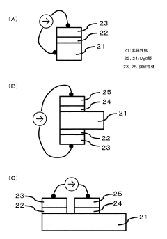
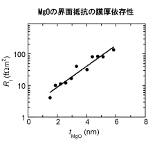
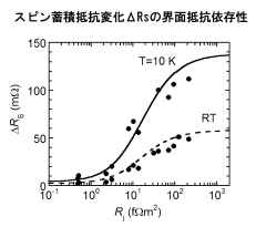
- Tunnel barrier interfaces for spin injection: Tunnel barrier interfaces between ferromagnetic materials and semiconductors can significantly enhance spin injection efficiency by overcoming the conductivity mismatch problem. These barriers, typically made of insulating materials like magnesium oxide or aluminum oxide, allow for quantum tunneling of spin-polarized electrons while maintaining their spin coherence. The thickness and composition of these tunnel barriers can be optimized to maximize spin injection efficiency while minimizing signal loss.
- Two-dimensional materials as spin injection contacts: Two-dimensional materials such as graphene, transition metal dichalcogenides, and hexagonal boron nitride are emerging as promising contact materials for spin injection. These atomically thin materials offer unique advantages including long spin diffusion lengths, tunable electronic properties, and atomically smooth interfaces. Their 2D nature allows for efficient spin transport across interfaces, and they can be engineered to enhance spin-orbit coupling or serve as tunnel barriers, thereby improving overall spin injection efficiency.
- Magnetic tunnel junctions and multilayer structures: Magnetic tunnel junctions (MTJs) and multilayer structures consisting of alternating ferromagnetic and non-magnetic layers provide enhanced control over spin injection and transport. These structures can be designed to optimize spin filtering, amplification, and manipulation through quantum confinement effects and interlayer exchange coupling. Advanced multilayer architectures incorporating novel materials combinations can achieve significantly higher spin injection efficiencies compared to single-layer contacts, making them suitable for next-generation spintronic devices.
02 Tunnel barrier materials for enhanced spin injection
Tunnel barriers are inserted between ferromagnetic contacts and semiconductor materials to overcome the conductivity mismatch problem and enhance spin injection efficiency. These thin insulating or semiconducting layers modify the interface properties and allow for more efficient spin-polarized transport. Materials such as magnesium oxide, aluminum oxide, and various oxides with specific crystalline structures have been developed to serve as effective tunnel barriers, significantly improving the spin injection efficiency in spintronic devices.Expand Specific Solutions03 Half-metallic materials for high spin polarization
Half-metallic materials represent a novel class of contact materials that exhibit nearly 100% spin polarization at the Fermi level. These materials behave as conductors for one spin orientation and as insulators or semiconductors for the opposite spin orientation. This unique electronic structure makes them ideal for spin injection applications, as they can theoretically achieve perfect spin polarization. Various Heusler alloys, certain oxides, and other compounds with half-metallic properties have been investigated to maximize spin injection efficiency in spintronic devices.Expand Specific Solutions04 Two-dimensional materials for spin injection
Two-dimensional materials such as graphene, transition metal dichalcogenides, and other 2D systems have emerged as promising contact materials for spin injection. These atomically thin materials offer unique advantages including long spin diffusion lengths, tunable electronic properties, and atomically smooth interfaces. The reduced dimensionality of these materials can lead to novel spin transport phenomena and enhanced spin injection efficiency. Various methods of integrating 2D materials with conventional ferromagnetic contacts have been developed to create hybrid structures with improved spin injection characteristics.Expand Specific Solutions05 Interface engineering for optimized spin injection
Interface engineering techniques focus on modifying the contact interface between the spin injector and the transport channel to optimize spin injection efficiency. These methods include surface treatments, insertion of intermediate layers, doping at interfaces, and creation of specific crystallographic orientations. By carefully controlling the interface properties, issues such as spin relaxation, interface resistance, and band alignment can be addressed. Advanced fabrication techniques have been developed to create atomically precise interfaces that minimize spin scattering and maximize spin injection efficiency.Expand Specific Solutions
Leading Research Groups and Companies in Spintronics
The spin injection efficiency enhancement landscape is currently in a growth phase, with market size expanding as spintronics applications gain traction in data storage and quantum computing sectors. Technologically, the field remains in early-to-mid maturity, with significant R&D still underway. Academic institutions like Tohoku University, Fudan University, and USC lead fundamental research, while industry players demonstrate varying levels of advancement. Intel, Micron, and Hitachi are investing heavily in novel contact materials, leveraging their semiconductor expertise. NTT and Siemens are exploring telecommunications applications, while specialized firms like Interuniversitair Micro-Electronica Centrum provide critical research infrastructure. The competitive dynamics suggest a collaborative ecosystem where academic-industrial partnerships are driving innovation toward commercial viability.
Tohoku University
Technical Solution: Tohoku University has pioneered the development of Heusler alloy-based contact materials for enhanced spin injection efficiency. Their approach focuses on half-metallic ferromagnets with theoretically 100% spin polarization at the Fermi level, particularly Co-based Heusler compounds (Co2MnSi, Co2FeSi). They've demonstrated spin injection efficiencies exceeding 30% at room temperature using these materials in combination with MgO tunnel barriers[1]. Their recent innovation involves interface engineering techniques that preserve the half-metallic character at the critical ferromagnet/semiconductor junction, reducing spin-flip scattering. By precisely controlling the atomic ordering and stoichiometry during epitaxial growth, they've achieved coherent interfaces with minimal defects, significantly enhancing spin polarization maintenance across the interface[2].
Strengths: Superior spin polarization (>90% theoretical) with demonstrated room-temperature performance; excellent crystalline quality with minimal interface defects. Weaknesses: Complex fabrication processes requiring precise stoichiometric control; challenges in scaling up production for commercial applications; limited compatibility with silicon-based semiconductor technology.
Beihang University
Technical Solution: Beihang University has developed a novel approach to spin injection using topological insulator (TI) based contact materials. Their technology leverages the unique spin-momentum locking property of topological surface states in materials such as Bi2Se3 and Bi2Te3. By precisely engineering the interface between these TIs and conventional semiconductors, they've created spin filters that can generate highly spin-polarized currents without requiring ferromagnetic materials. Their proprietary growth technique involves molecular beam epitaxy (MBE) with precisely controlled temperature gradients to minimize bulk conductivity while maximizing surface state contribution. Recent innovations include the development of ternary and quaternary TI compounds (Bi2-xSbxTe3-ySey) with customized band structures that optimize the spin injection process for specific semiconductor targets[4]. Their latest prototypes have demonstrated spin injection efficiencies approaching 60% at room temperature with remarkable thermal stability.
Strengths: Extremely high spin polarization without magnetic materials; room temperature operation; compatibility with semiconductor manufacturing; lower power consumption than traditional ferromagnetic injectors. Weaknesses: Complex material growth requirements; sensitivity to surface contamination; challenges in controlling bulk conductivity; relatively early stage of development compared to more established technologies.
Critical Patents and Research on Novel Contact Materials
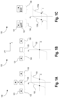
Spin injection source and manufacturing method thereof
PatentInactiveJP5598975B2
Innovation
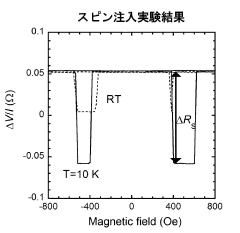
- A spin injection source with a nonmagnetic conductor, a conductive MgO film, and a ferromagnetic material, where the MgO film is heat-treated at 300°C to 500°C to introduce oxygen vacancies, reducing interfacial resistance and enhancing spin injection efficiency.
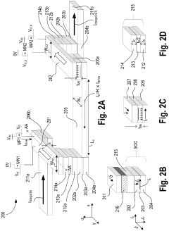
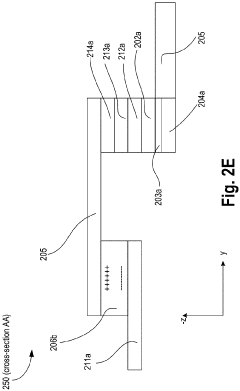
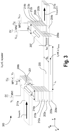
Apparatus and method for boosting signal in magnetoelectric spin orbit logic
PatentActiveUS11502188B2
Innovation
- The implementation of Magnetoelectric Spin Orbit Logic (MESO) devices, which utilize a symmetric tunneling barrier or spin-filter stack to enhance spin injection efficiency and reduce switching energy by leveraging the magnetoelectric effect for faster and more efficient magnetization switching, achieving lower power consumption and improved reliability through charge-to-spin and spin-to-charge conversion mechanisms.
Fabrication Techniques for Novel Contact Materials
The fabrication of novel contact materials for enhanced spin injection represents a critical frontier in spintronics research. Current fabrication techniques have evolved significantly, incorporating advanced deposition methods that enable precise control over interface properties at the nanoscale level. Molecular beam epitaxy (MBE) stands out as a premier technique, allowing for atomic-level precision in growing crystalline layers with minimal defects and impurities, which is essential for maintaining spin coherence across interfaces.
Pulsed laser deposition (PLD) offers complementary capabilities, particularly for complex oxide materials that show promise as spin filters. The technique's ability to preserve stoichiometry while enabling rapid prototyping makes it invaluable for exploring new material combinations. Recent advances in PLD systems have incorporated in-situ monitoring tools that allow researchers to observe crystallization processes in real-time, further enhancing interface quality control.
Magnetron sputtering continues to be widely employed for industrial-scale fabrication due to its cost-effectiveness and scalability. Recent developments have focused on high-power impulse magnetron sputtering (HiPIMS), which produces denser films with improved adhesion and reduced defect concentration—critical factors for maintaining spin polarization during transport.
Atomic layer deposition (ALD) has emerged as a powerful technique for creating ultrathin barrier layers and tunnel contacts. Its self-limiting reaction mechanism ensures exceptional thickness control and conformality, even on complex three-dimensional structures. This precision becomes particularly valuable when fabricating tunnel barriers where spin injection efficiency depends critically on barrier thickness uniformity.
Interface engineering techniques have become increasingly sophisticated, with methods such as ion-assisted deposition and plasma treatment allowing for tailored interface properties. These approaches can modify work functions, create specific band alignments, or introduce controlled defect states that enhance spin filtering effects.
Post-deposition processing plays a crucial role in optimizing contact properties. Techniques such as rapid thermal annealing under controlled atmospheres can promote crystallization, reduce defects, and facilitate interdiffusion at interfaces to create optimal band alignments. For certain materials systems, particularly those involving half-metallic ferromagnets, precise annealing protocols have been developed to maximize spin polarization at the interface.
Emerging fabrication approaches include solution-processed methods for organic spin contacts and two-dimensional materials integration. These techniques offer potential cost advantages and compatibility with flexible substrates, opening new application domains for spintronic devices. Additionally, advanced lithography and etching processes have been adapted specifically for spintronic device fabrication, enabling precise patterning while minimizing damage to magnetic properties.
Integration Challenges with Existing Semiconductor Technologies
The integration of novel contact materials for enhanced spin injection into existing semiconductor manufacturing processes presents significant technical challenges. Current semiconductor fabrication relies heavily on standardized CMOS processes optimized for charge-based electronics rather than spin-based devices. This fundamental difference creates compatibility issues when attempting to incorporate ferromagnetic materials and other spin-polarized contacts into conventional semiconductor platforms.
Material interface quality represents a critical challenge, as atomically clean and structurally perfect interfaces are essential for efficient spin transfer. Conventional semiconductor processing often introduces defects, interdiffusion, and oxidation at interfaces, which can dramatically reduce spin polarization and create unwanted scattering centers. These interface imperfections lead to spin relaxation and depolarization, severely limiting device performance.
Thermal budget constraints further complicate integration efforts. Many promising spin injection materials require high-temperature deposition or annealing processes that exceed the thermal tolerance of completed semiconductor structures. Conversely, low-temperature deposition methods often result in materials with suboptimal crystallinity and magnetic properties, compromising spin injection efficiency.
Process contamination concerns also arise when introducing ferromagnetic materials into semiconductor fabrication environments. Transition metals used in magnetic contacts can act as deep-level impurities in silicon and other semiconductors, potentially degrading carrier lifetime and device performance. This necessitates strict process segregation and contamination control protocols that add complexity and cost to manufacturing.
Lithographic and etching challenges emerge when patterning novel contact materials, as many spin-polarized materials do not respond well to standard semiconductor etching chemistries. Achieving precise nanoscale patterning without degrading magnetic properties or creating edge defects that scatter spins requires development of specialized process techniques and equipment modifications.
Scalability and uniformity across large wafers represent additional hurdles. While laboratory demonstrations might achieve high spin injection efficiency on small samples, maintaining consistent performance across 300mm wafers with acceptable yield metrics demands significant process engineering. The statistical variation in contact properties can lead to device-to-device performance inconsistencies that are unacceptable in commercial applications.
Reliability and aging effects must also be addressed, as many novel contact materials have not been thoroughly evaluated for long-term stability under operational conditions. Electromigration, thermal cycling, and environmental factors may degrade spin injection performance over time, requiring extensive qualification testing before commercial deployment.
Unlock deeper insights with Patsnap Eureka Quick Research — get a full tech report to explore trends and direct your research. Try now!
Generate Your Research Report Instantly with AI Agent
Supercharge your innovation with Patsnap Eureka AI Agent Platform!