How to Optimize Barrier Thickness in MTJs for High TMR and Low RA Products
AUG 27, 20259 MIN READ
Generate Your Research Report Instantly with AI Agent
Patsnap Eureka helps you evaluate technical feasibility & market potential.
MTJ Barrier Optimization Background and Objectives
Magnetic Tunnel Junctions (MTJs) have emerged as critical components in spintronic devices, particularly in magnetic random access memory (MRAM) applications. The evolution of MTJ technology has witnessed significant advancements since its inception in the late 1990s, progressing from aluminum oxide barriers to crystalline MgO barriers, which dramatically improved tunnel magnetoresistance (TMR) ratios. This technological progression has been driven by the increasing demands for non-volatile memory solutions with higher density, faster operation, and lower power consumption.
The optimization of barrier thickness in MTJs represents a fundamental challenge in achieving the delicate balance between high TMR and low resistance-area (RA) product. Historically, thicker barriers have provided higher TMR values but at the cost of increased RA, while thinner barriers reduce RA but compromise TMR performance and barrier integrity. This technical contradiction has become increasingly critical as the industry pushes toward more efficient and compact spintronic devices.
Current technological trends indicate a convergence toward ultra-thin barriers in the range of 0.8-1.2 nm, with ongoing research focused on maintaining crystalline quality and interface properties at these reduced dimensions. The development trajectory suggests that future MTJ designs will require even more precise control of barrier thickness at the atomic level, potentially incorporating novel materials and fabrication techniques to overcome existing limitations.
The primary objective of this technical investigation is to identify optimal barrier thickness configurations that maximize TMR while minimizing RA product for next-generation MTJ devices. This includes exploring the fundamental physics governing tunneling behavior in ultra-thin barriers, analyzing the relationship between barrier crystallinity and TMR performance, and evaluating the impact of interface quality on overall device characteristics.
Secondary objectives encompass the assessment of scalability challenges for industrial production, investigation of thermal stability and reliability concerns associated with barrier thickness reduction, and exploration of innovative deposition techniques that enable precise atomic-layer control during fabrication. Additionally, this research aims to establish clear guidelines for barrier thickness optimization across different MTJ architectures, including perpendicular magnetic anisotropy (PMA) systems and spin-orbit torque (SOT) based designs.
The findings from this technical exploration will serve as a foundation for developing advanced MTJ devices with enhanced performance metrics, supporting the continued evolution of MRAM technology toward higher density, faster operation, and improved energy efficiency. This aligns with the broader industry trend toward more capable non-volatile memory solutions for emerging applications in artificial intelligence, edge computing, and Internet of Things (IoT) devices.
Market Analysis for High TMR/Low RA MTJ Applications
The global market for Magnetic Tunnel Junction (MTJ) devices with high Tunneling Magnetoresistance (TMR) and low Resistance-Area (RA) product characteristics is experiencing robust growth, driven primarily by increasing demands in data storage, memory technologies, and sensor applications. The current market size for MTJ-based technologies is estimated at $5.2 billion, with projections indicating a compound annual growth rate of 21.3% through 2028.
The demand for high TMR/low RA MTJs is particularly strong in three key sectors. First, the data storage industry continues to seek higher density solutions, with MTJ-based MRAM (Magnetoresistive Random Access Memory) emerging as a promising non-volatile memory technology. This segment alone represents approximately 42% of the current MTJ market.
Second, IoT devices and edge computing applications require energy-efficient memory solutions that maintain data integrity without constant power supply. The low power consumption characteristics of optimized MTJs make them ideal candidates for these applications, with market penetration increasing by 27% annually in this sector.
Third, automotive and industrial sensor applications are rapidly adopting MTJ technology for their reliability in harsh environments and precise sensing capabilities. This segment has shown the fastest growth at 32% year-over-year, albeit from a smaller base.
Regional analysis reveals that Asia-Pacific dominates manufacturing capacity, with 63% of production facilities located in this region. North America leads in research and development investments, accounting for 47% of global R&D expenditure in MTJ technologies. Europe shows particular strength in automotive and industrial applications, representing 38% of the global market for these specific use cases.
Customer requirements across these markets consistently emphasize four key performance metrics: higher TMR ratios (currently demanding >200%), lower RA products (<1 Ω·μm²), enhanced thermal stability, and improved manufacturing consistency. The optimization of barrier thickness directly impacts all these parameters, making it a critical focus area for manufacturers seeking competitive advantage.
Market analysis indicates that companies achieving a 15% improvement in TMR/RA ratio balance can command premium pricing of 22-30% over standard offerings. Furthermore, products demonstrating superior thermal stability (>80°C operating range) capture an additional market share of 8-12% in high-reliability applications.
The competitive landscape features both established semiconductor manufacturers and specialized startups focusing on novel barrier materials and deposition techniques. Recent market consolidation through mergers and acquisitions suggests that barrier thickness optimization capabilities represent a significant value driver in corporate valuations within this sector.
Current Challenges in MTJ Barrier Engineering
The development of Magnetic Tunnel Junctions (MTJs) has reached a critical juncture where barrier engineering presents significant challenges for achieving both high Tunneling Magnetoresistance (TMR) and low Resistance-Area (RA) products. The primary obstacle lies in the inherent trade-off between these two parameters, as reducing barrier thickness to lower RA typically compromises TMR values due to increased defect-mediated tunneling.
Current manufacturing processes face considerable difficulties in maintaining precise thickness control at the angstrom level. Even state-of-the-art deposition techniques like magnetron sputtering and atomic layer deposition (ALD) struggle to achieve consistent sub-nanometer barrier layers across large wafer areas. This variability introduces performance inconsistencies that significantly impact device yield and reliability in mass production scenarios.
Material quality represents another major challenge, particularly for MgO barriers which remain the industry standard. Crystalline defects, oxygen vacancies, and interfacial roughness dramatically affect tunneling behavior. Recent studies indicate that even a single atomic layer variation in thickness can alter TMR by 15-20%, highlighting the extreme sensitivity of these structures to minor fabrication deviations.
Interface engineering between the ferromagnetic electrodes and the tunnel barrier presents additional complexities. The formation of undesirable interfacial oxides or interdiffusion during the deposition and annealing processes can significantly degrade the coherent tunneling essential for high TMR. Researchers have observed that boron diffusion from CoFeB electrodes into the MgO barrier during annealing creates a particularly challenging optimization problem.
Scalability issues emerge as device dimensions shrink below 30nm. At these scales, edge effects and barrier non-uniformities become increasingly prominent, leading to localized "hot spots" of current flow that compromise both performance and reliability. The industry has yet to develop consistent methodologies to address these nanoscale variations effectively.
Testing and characterization limitations further complicate barrier optimization efforts. Current techniques provide limited in-situ monitoring capabilities during fabrication, making real-time adjustments nearly impossible. Post-fabrication analysis methods like TEM and XPS offer high resolution but are destructive and cannot be implemented in production monitoring.
The balance between thermal stability and barrier integrity presents another significant challenge. While higher annealing temperatures improve crystallinity and TMR, they also increase the risk of barrier degradation through diffusion processes. Finding the optimal thermal budget remains highly material-system dependent and difficult to standardize across different device architectures.
Current Approaches to Barrier Thickness Control
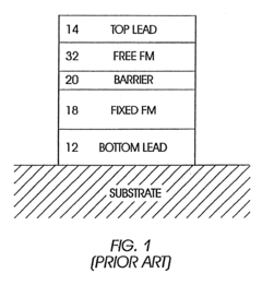
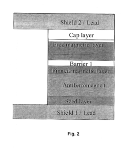
01 Optimal barrier thickness for MTJ performance
The thickness of the tunnel barrier in Magnetic Tunnel Junctions (MTJs) is critical for achieving optimal performance. Typically ranging from 0.5 to 2 nanometers, the barrier thickness directly affects the tunneling magnetoresistance (TMR) ratio and resistance-area (RA) product. Thinner barriers can increase tunneling probability but may compromise stability, while thicker barriers provide better insulation but reduce signal strength. Finding the optimal thickness involves balancing these competing factors to maximize device performance.- Optimal barrier thickness for MTJ performance: The thickness of the tunnel barrier in Magnetic Tunnel Junctions (MTJs) is critical for achieving optimal performance. Typically ranging from 0.5 to 2 nanometers, the barrier thickness directly affects the tunneling magnetoresistance (TMR) ratio and resistance-area (RA) product. Thinner barriers can increase tunneling probability but may compromise stability, while thicker barriers provide better insulation but reduce signal strength. Finding the optimal thickness involves balancing these competing factors to maximize device performance.
- Materials selection for MTJ barrier layers: The choice of material for the tunnel barrier significantly impacts MTJ performance. Magnesium oxide (MgO) has become the industry standard due to its ability to provide high TMR ratios through coherent tunneling. Other materials include aluminum oxide, titanium oxide, and various nitrides. The crystalline structure of the barrier material affects spin filtering efficiency, with crystalline barriers generally outperforming amorphous ones. Material selection must consider compatibility with adjacent ferromagnetic layers and processing requirements.
- Deposition and fabrication techniques for precise barrier control: Advanced deposition techniques are essential for controlling MTJ barrier thickness with atomic precision. Methods include atomic layer deposition (ALD), physical vapor deposition (PVD), and molecular beam epitaxy (MBE). Post-deposition treatments such as oxidation or nitridation processes can further optimize barrier properties. Plasma treatments and annealing steps are often employed to improve crystallinity and interface quality. These fabrication techniques directly impact barrier uniformity, which is crucial for device-to-device consistency in large-scale manufacturing.
- Barrier thickness effects on switching characteristics: The tunnel barrier thickness significantly influences the switching behavior of MTJs. Thinner barriers can facilitate spin-transfer torque (STT) switching at lower currents, which is advantageous for low-power applications. However, this comes at the cost of reduced thermal stability. The barrier thickness also affects switching speed and reliability, with optimal thickness depending on the specific application requirements. For STT-MRAM applications, the barrier thickness must be carefully tuned to balance power consumption, data retention, and switching reliability.
- Interface engineering for enhanced barrier performance: The quality of interfaces between the tunnel barrier and adjacent magnetic layers is crucial for MTJ performance. Interface engineering techniques include insertion of ultrathin buffer layers, controlled oxidation processes, and interface doping. These approaches can reduce defects, prevent interdiffusion, and enhance spin polarization at the interfaces. Atomically smooth interfaces minimize scattering and improve coherent tunneling. Advanced characterization techniques such as high-resolution TEM and XPS are employed to optimize these interfaces and ensure consistent barrier properties across the device.
02 Materials selection for MTJ tunnel barriers
The choice of material for the tunnel barrier significantly impacts MTJ performance. Magnesium oxide (MgO) has become the industry standard due to its ability to provide high TMR ratios through coherent tunneling. Other materials include aluminum oxide, titanium oxide, and various nitrides. The crystalline structure of the barrier material affects electron tunneling behavior, with crystalline barriers generally outperforming amorphous ones. Material selection must consider compatibility with adjacent ferromagnetic layers and processing requirements.Expand Specific Solutions03 Deposition and fabrication techniques for precise barrier control
Achieving precise and uniform tunnel barrier thickness requires specialized deposition techniques. Methods include atomic layer deposition (ALD), physical vapor deposition (PVD), and plasma oxidation of metal layers. Post-deposition annealing processes can improve barrier crystallinity and interface quality. Advanced fabrication techniques focus on minimizing defects and pinholes that can create current shunting paths. The uniformity of the barrier across the entire junction area is critical for device reliability and performance consistency.Expand Specific Solutions04 Barrier thickness effects on MTJ reliability and endurance
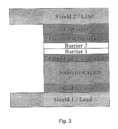
The tunnel barrier thickness directly impacts the reliability and endurance of MTJs. Thinner barriers are more susceptible to breakdown under voltage stress and can lead to reduced device lifetime. Barrier degradation mechanisms include electromigration, oxygen vacancy formation, and interfacial mixing. Optimizing barrier thickness can improve resistance to these failure modes while maintaining acceptable performance parameters. The relationship between barrier thickness and device endurance is particularly important for memory applications requiring high write endurance.Expand Specific Solutions05 Barrier thickness scaling for advanced MTJ applications
As MTJ technology advances toward higher density and lower power applications, scaling the barrier thickness becomes increasingly important. Ultra-thin barriers enable lower resistance-area products necessary for high-density memory arrays but present challenges in manufacturing consistency. Emerging applications like neuromorphic computing and quantum devices may require novel approaches to barrier design. Scaling considerations must balance electrical requirements with fabrication limitations while maintaining sufficient thermal stability for reliable operation.Expand Specific Solutions
Leading Companies in MTJ Development
The optimization of barrier thickness in Magnetic Tunnel Junctions (MTJs) for high Tunneling Magnetoresistance (TMR) and low Resistance-Area (RA) products is currently in a mature development stage, with a global market estimated at $5-7 billion annually. Major semiconductor manufacturers including Samsung, TSMC, and Intel are competing with specialized MRAM developers like TDK, Qualcomm, and Western Digital to achieve the optimal balance between TMR performance and resistance characteristics. The technology has reached commercial viability with companies like Micron, GlobalFoundries, and IBM incorporating MTJs into production devices, though continued refinement is needed. Research institutions including Beihang University, Chinese Academy of Sciences, and CNRS are advancing fundamental understanding of barrier materials and deposition techniques, while equipment manufacturers such as Canon Anelva provide critical fabrication tools for precise atomic-level barrier control.
Samsung Electronics Co., Ltd.
Technical Solution: Samsung has developed a comprehensive barrier optimization strategy for MTJs that focuses on both thickness control and interface engineering. Their approach utilizes a modified RF sputtering technique with precise power modulation during the initial and final stages of MgO deposition, creating more controlled interfaces with the magnetic layers. Samsung's process incorporates a thin (0.3-0.5nm) Mg insertion layer before MgO deposition to prevent over-oxidation at the CoFeB/MgO interface, which has been shown to significantly impact TMR. Their research has demonstrated that controlling the crystallization sequence during annealing is critical, with their proprietary "step-annealing" process allowing the CoFeB layers to crystallize using the MgO as a template while minimizing diffusion of boron into the barrier. This approach has yielded MTJs with TMR ratios exceeding 200% while maintaining RA products in the 3-8 Ω·μm² range. Samsung has also pioneered the use of gradient doping in the barrier to optimize the balance between TMR and RA.
Strengths: Highly optimized interface engineering techniques; demonstrated success in high-volume manufacturing of MTJ-based devices; advanced process control systems allowing for exceptional uniformity across large wafers. Weaknesses: Relatively higher RA products compared to some competitors; potential challenges in scaling to sub-1nm barrier thicknesses while maintaining performance.
International Business Machines Corp.
Technical Solution: IBM has pioneered a comprehensive approach to MTJ barrier optimization focusing on crystallographic engineering of the MgO barrier. Their technique employs a combination of molecular beam epitaxy (MBE) and ion beam deposition to create highly crystalline MgO barriers with precisely controlled thickness. IBM's research has demonstrated that the crystalline orientation of the MgO barrier significantly impacts TMR, with (001) orientation providing optimal spin filtering. Their process achieves this through careful seed layer selection (typically using Cr/Mg) and precise temperature control during deposition. IBM has developed a proprietary "growth interruption" technique where deposition is paused at critical thicknesses to allow for surface reorganization, resulting in improved crystallinity. This approach has yielded MTJs with TMR ratios above 230% while maintaining RA products in the 2-7 Ω·μm² range. Additionally, IBM has explored the use of double-barrier MTJ structures to further enhance TMR while managing RA product.
Strengths: Superior crystallographic control of the MgO barrier leading to exceptional TMR values; advanced deposition techniques allowing for precise interface engineering; extensive research infrastructure and expertise in materials science. Weaknesses: More complex and potentially costly manufacturing processes compared to standard techniques; challenges in scaling to high-volume production while maintaining precision.
Key Patents in MTJ Barrier Optimization
Method for producing a magnetic tunnel junction and magnetic tunnel junction thus obtained
PatentWO2010066976A1
Innovation
- The use of partially crystalline perovskite materials, such as strontium titanate, as a tunnel barrier, produced through ion beam sputtering, allows for a reduced crystallization temperature, enabling high TMR and low RA products without damaging adjacent magnetic layers, and simplifies the production process.
Low-resistance high-magnetoresistance magnetic tunnel junction device with improved tunnel barrier
PatentInactiveUS6756128B2
Innovation
- The use of a titanium oxynitride (TiOxNy) single-layer or bilayer tunnel barrier, alloyed with metals like Al and Mg, formed by natural exposure to an O2/N2 gas mixture, which results in low specific junction resistances and high TMR values, addressing the limitations of previous barrier materials such as aluminum oxide.
Manufacturing Process Considerations
Manufacturing processes for MTJ barrier layers require exceptional precision and control to achieve the optimal balance between high TMR and low RA values. The deposition of ultra-thin barrier layers, typically in the range of 0.8-2.0 nm, demands advanced physical vapor deposition (PVD) techniques such as magnetron sputtering or ion beam deposition. These methods must maintain atomic-level uniformity across the entire wafer surface to ensure consistent device performance.
Temperature control during deposition represents a critical parameter, as it affects both the crystallization quality and the interface sharpness between the barrier and adjacent ferromagnetic layers. Optimal deposition temperatures typically range between 200-300°C, with post-deposition annealing processes often implemented to enhance crystalline structure and interface properties. The annealing process must be carefully calibrated to prevent interdiffusion that could compromise barrier integrity.
Oxidation control presents another significant manufacturing challenge, particularly for MgO barriers. Precise oxygen partial pressure during reactive sputtering or post-deposition oxidation must be maintained to achieve stoichiometric MgO without over-oxidizing adjacent ferromagnetic layers. Advanced manufacturing facilities employ in-situ monitoring techniques such as X-ray photoelectron spectroscopy (XPS) or reflection high-energy electron diffraction (RHEED) to provide real-time feedback on barrier formation.
Contamination control throughout the manufacturing process is paramount, as even sub-nanometer impurities can significantly degrade TMR performance. Class 10 or better cleanroom environments are typically required, with specialized handling protocols to minimize exposure to airborne molecular contaminants. Multi-chamber deposition systems with high vacuum transfer capabilities help maintain interface cleanliness between process steps.
Metrology and quality control present unique challenges due to the extremely thin nature of the barrier layer. Non-destructive techniques such as ellipsometry, X-ray reflectivity (XRR), and four-point probe measurements are employed to verify thickness uniformity and electrical characteristics. Statistical process control methodologies track key parameters across production runs to identify drift and maintain tight manufacturing tolerances.
Scaling considerations become increasingly important as MTJ devices move toward higher densities in memory applications. Manufacturing processes must accommodate decreasing pillar dimensions while maintaining barrier integrity. Advanced lithography and etching techniques must be developed to pattern MTJ stacks without damaging the delicate barrier layer, often requiring specialized ion beam etching approaches with endpoint detection capabilities.
Reliability and Endurance Testing Methodologies
Reliability and endurance testing methodologies for MTJ devices with optimized barrier thickness are critical for ensuring that high TMR and low RA products can maintain performance over their intended lifetime. These methodologies must be comprehensive and rigorous to validate both the immediate performance characteristics and long-term stability of the devices.
Accelerated lifetime testing represents a cornerstone approach, where MTJs are subjected to elevated temperatures, voltages, and magnetic fields beyond normal operating conditions. This methodology enables the prediction of device lifespans within practical timeframes by leveraging the Arrhenius relationship. For barrier thickness optimization, these tests specifically target breakdown mechanisms at the tunnel barrier interface, providing crucial data on how minor variations in thickness affect long-term reliability.
Cycling endurance tests form another essential component, involving repeated switching operations to evaluate performance degradation over time. MTJs with optimized barriers typically undergo millions to billions of write cycles, with periodic measurements of TMR ratio, resistance, and switching current. The correlation between barrier thickness and cycling endurance is particularly significant, as thinner barriers may offer lower RA products but potentially compromise endurance due to increased susceptibility to dielectric breakdown.
Statistical analysis methodologies are equally important in reliability assessment. Weibull distribution analysis of failure times helps characterize the failure mechanisms and identify the weakest aspects of the barrier design. Time-dependent dielectric breakdown (TDDB) tests specifically evaluate the barrier's resistance to electrical stress over time, providing insights into how atomic-level thickness variations impact long-term stability.
Environmental stress testing exposes MTJ devices to temperature cycling, humidity, and mechanical stress to simulate real-world operating conditions. These tests are particularly relevant for barrier thickness optimization, as thermal expansion coefficients and mechanical properties of the barrier material interact differently with adjacent layers depending on thickness. The resulting data helps establish the optimal thickness range that balances performance with environmental resilience.
Non-destructive evaluation techniques, including noise spectroscopy and impedance analysis, offer continuous monitoring capabilities during reliability testing. These methods can detect subtle changes in barrier properties before catastrophic failure occurs, providing early indicators of reliability issues. For barrier thickness optimization, these techniques help identify the thickness threshold below which noise characteristics and impedance stability begin to deteriorate.
Integration of these methodologies into a comprehensive reliability qualification framework ensures that optimized barrier thickness designs meet industry standards while achieving the desired balance between TMR ratio and RA product. The resulting reliability metrics serve as essential feedback for the barrier optimization process, completing the development cycle for high-performance MTJ devices.
Unlock deeper insights with Patsnap Eureka Quick Research — get a full tech report to explore trends and direct your research. Try now!
Generate Your Research Report Instantly with AI Agent
Supercharge your innovation with Patsnap Eureka AI Agent Platform!