

How to Optimize OLED Pixel Density for High-Resolution Screens
SEP 12, 20259 MIN READ
Generate Your Research Report Instantly with AI Agent
Patsnap Eureka helps you evaluate technical feasibility & market potential.
OLED Pixel Density Evolution and Objectives
Organic Light-Emitting Diode (OLED) technology has undergone remarkable evolution since its inception in the late 1980s. The journey began with rudimentary displays featuring limited pixel densities of under 100 pixels per inch (PPI), primarily constrained by manufacturing capabilities and material limitations. By the early 2000s, OLED displays started appearing in consumer electronics with modest resolutions, marking the beginning of commercial viability for this technology.
The mid-2010s witnessed a paradigm shift with the introduction of high-definition OLED panels exceeding 300 PPI, revolutionizing mobile device displays. This advancement was facilitated by breakthroughs in thin-film transistor (TFT) backplane technologies and precision deposition methods. The industry subsequently progressed to ultra-high-definition displays with pixel densities surpassing 500 PPI, enabling virtual reality applications and premium smartphone displays with unprecedented visual fidelity.
Current technological frontiers are pushing toward extreme pixel densities exceeding 1000 PPI, particularly for near-eye display applications in augmented and virtual reality systems. This progression reflects the industry's response to increasing consumer expectations for immersive visual experiences and the elimination of the "screen door effect" in close-viewing scenarios.
The optimization of OLED pixel density is driven by several interconnected objectives. Primary among these is the achievement of visual perfection through pixel imperceptibility—reaching the threshold where individual pixels become indistinguishable to the human eye under normal viewing conditions. This threshold varies based on viewing distance, with higher densities required for near-eye displays compared to televisions viewed from several feet away.
Energy efficiency represents another critical objective, as higher pixel counts traditionally correlate with increased power consumption—a particular concern for battery-powered devices. Manufacturers aim to balance visual quality with practical power constraints through innovative pixel architectures and driving schemes.
Manufacturing yield and cost-effectiveness constitute significant considerations, as extremely high pixel densities introduce production challenges related to precision deposition, defect rates, and material utilization. The industry seeks to develop scalable production methods that maintain economic viability while advancing technical capabilities.
Future objectives include developing novel sub-pixel arrangements that maximize perceived resolution while minimizing actual pixel count, exploring quantum dot-enhanced OLED technologies for improved color gamut at higher densities, and investigating micro-LED hybrid approaches that combine the benefits of both display technologies for next-generation high-resolution applications.
Market Demand for High-Resolution OLED Displays
The global market for high-resolution OLED displays has experienced exponential growth over the past decade, driven primarily by consumer electronics, particularly smartphones and premium televisions. Market research indicates that the high-resolution OLED display market reached approximately $32 billion in 2022, with projections suggesting growth to $58 billion by 2027, representing a compound annual growth rate of 12.6%.
Consumer demand for superior visual experiences continues to be the primary market driver. End users increasingly expect displays that offer higher pixel densities, with the premium smartphone segment now routinely featuring pixel densities exceeding 500 PPI (pixels per inch). This trend extends beyond mobile devices to larger formats including televisions, monitors, and automotive displays, where OLED technology's superior contrast ratios and color reproduction provide competitive advantages.
The virtual reality (VR) and augmented reality (AR) segments represent particularly demanding use cases for high-resolution OLED displays. These applications require pixel densities approaching 1000 PPI to eliminate the "screen door effect" that diminishes immersion. Market analysis shows the AR/VR display segment growing at 24% annually, significantly outpacing the broader display market.
Professional markets including medical imaging, design, and content creation are emerging as significant demand drivers for ultra-high-resolution OLED displays. These sectors prioritize color accuracy, contrast, and resolution over cost considerations, creating premium market segments with higher profit margins.
Regional analysis reveals Asia-Pacific as the dominant market for high-resolution OLED displays, accounting for 63% of global demand. This concentration stems from the region's manufacturing ecosystem and consumer adoption rates. North America and Europe follow with 18% and 14% market share respectively, with particularly strong demand in premium and professional segments.
Industry surveys indicate that consumers rank display quality among the top three purchase considerations for smartphones and televisions. This prioritization has intensified competition among device manufacturers to implement higher-resolution displays as key differentiating features in their flagship products.
The foldable display segment presents a specialized but rapidly growing market for high-resolution OLEDs. This application introduces unique technical challenges for maintaining pixel density across flexible substrates. Market data shows foldable device shipments increasing by 75% year-over-year, creating demand for specialized high-resolution OLED solutions that can maintain visual quality while accommodating mechanical stress.
Battery life considerations in mobile devices create countervailing pressure against ever-increasing pixel densities. Market research indicates that 68% of consumers cite battery life as a critical purchase factor, creating a complex optimization challenge for manufacturers balancing visual quality against power consumption.
Current OLED Pixel Density Limitations
Despite significant advancements in OLED technology, current pixel density limitations present substantial challenges for high-resolution display development. The physical constraints of OLED subpixel structures create fundamental barriers to achieving ultra-high pixel densities. Most commercial OLED displays currently max out at 600-800 PPI (pixels per inch) for mobile devices, with specialized applications reaching approximately 1,000 PPI. Beyond these thresholds, manufacturing yield rates decline dramatically while production costs increase exponentially.
The RGB subpixel arrangement in OLED panels requires each pixel to contain separate red, green, and blue light-emitting components, consuming valuable panel real estate. This physical requirement creates a natural ceiling for how densely pixels can be packed before electrical interference and heat dissipation issues emerge. Additionally, as pixel size decreases, the precision requirements for deposition processes increase substantially, pushing against the limits of current manufacturing equipment capabilities.
Power efficiency represents another critical limitation. Higher pixel densities necessitate smaller individual pixels, which typically operate at lower efficiency levels due to increased current density and thermal constraints. This efficiency reduction creates a negative feedback loop where displays require more power to maintain brightness, generating additional heat that further compromises pixel performance and lifespan.
Manufacturing challenges compound these issues. Current fine metal mask (FMM) deposition techniques struggle with alignment precision below certain pixel sizes, typically around 2-3 micrometers. Alternative approaches like inkjet printing offer potential solutions but face their own limitations in consistency and scalability for mass production. The industry has reached a point where incremental improvements in traditional manufacturing processes yield diminishing returns for pixel density enhancement.
Electrical crosstalk between densely packed pixels presents another significant barrier. As pixels move closer together, signal interference increases, potentially causing color bleeding and reduced image clarity—ironically undermining the very purpose of higher resolution displays. Current thin-film transistor (TFT) backplane technologies also face limitations in how many pixels they can effectively address at extremely high densities.
Material science constraints further complicate density improvements. The organic materials in OLEDs have inherent limitations in current handling capacity and operational stability at extremely small scales. While new materials show promise, their commercial viability and integration into existing manufacturing processes remain challenging hurdles for immediate implementation in ultra-high-density displays.
Current Pixel Density Optimization Approaches
01 High-resolution OLED display technologies
Various technologies have been developed to achieve high pixel density in OLED displays. These include specialized pixel arrangements, sub-pixel structures, and manufacturing techniques that enable increased resolution while maintaining display quality. High-resolution OLED displays are particularly important for applications requiring detailed image reproduction such as virtual reality, augmented reality, and high-end mobile devices.- High-resolution OLED display technologies: Various technologies have been developed to achieve high pixel density in OLED displays. These include specialized pixel arrangements, sub-pixel structures, and manufacturing techniques that enable displays with increased resolution while maintaining image quality. High-resolution OLED displays are particularly important for applications requiring detailed image reproduction such as virtual reality, augmented reality, and high-end mobile devices.
- Pixel circuit designs for high-density OLED displays: Advanced pixel circuit designs are crucial for achieving high pixel density in OLED displays. These circuits control the current flow to each pixel, ensuring uniform brightness and color accuracy across the display. Innovations in circuit design include compensation mechanisms for threshold voltage variations, improved driving schemes, and integration of additional transistors to enhance pixel performance while minimizing the circuit footprint.
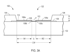
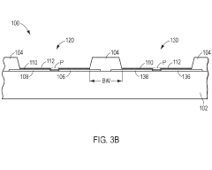
- Manufacturing methods for high-density OLED pixels: Specialized manufacturing techniques have been developed to produce OLED displays with increased pixel density. These methods include advanced patterning processes, precise deposition techniques for organic materials, and innovative approaches to electrode formation. Manufacturing innovations focus on reducing pixel size while maintaining electrical performance and preventing issues such as cross-talk between adjacent pixels.
- Compensation techniques for high-density displays: As pixel density increases, various compensation techniques become necessary to maintain display quality. These include methods to address non-uniformity in brightness, color shifts, and aging effects that become more pronounced in high-density displays. Advanced algorithms and hardware solutions work together to detect and compensate for these variations, ensuring consistent visual performance throughout the display's lifetime.
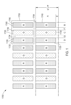
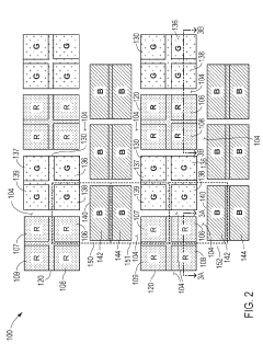
- Sub-pixel arrangements for enhanced pixel density: Innovative sub-pixel arrangements allow for increased effective resolution without proportionally increasing the number of pixels. These designs include various RGB sub-pixel layouts, PenTile matrix arrangements, and other non-standard configurations that optimize the perceived resolution while managing manufacturing constraints. By strategically positioning sub-pixels, these arrangements can achieve higher apparent pixel density while maintaining manufacturability.
02 Pixel circuit designs for high-density OLED displays
Advanced pixel circuit designs are crucial for achieving high pixel density in OLED displays. These circuits control the current flow to individual pixels, ensuring uniform brightness and color accuracy across the display. Innovations in circuit design include compensation mechanisms for threshold voltage variations, improved driving schemes, and compact transistor arrangements that allow for smaller pixel sizes while maintaining performance.Expand Specific Solutions03 Manufacturing methods for high-density OLED pixels
Specialized manufacturing techniques have been developed to produce high-density OLED displays. These include advanced photolithography processes, fine metal mask technology, and innovative deposition methods that enable the creation of smaller pixel structures. These manufacturing methods address challenges such as maintaining color purity, preventing cross-contamination between adjacent pixels, and ensuring consistent performance across the display.Expand Specific Solutions04 Compensation techniques for high-density displays
As pixel density increases, various compensation techniques become necessary to maintain display quality. These include methods to address non-uniformity issues, pixel aging compensation, and techniques to reduce power consumption while maintaining brightness. Advanced algorithms and hardware solutions work together to ensure consistent performance across the display despite the challenges posed by high pixel density.Expand Specific Solutions05 Pixel structure innovations for improved density
Novel pixel structures have been developed to increase the density of OLED displays. These include innovations in sub-pixel arrangements, shared electrode designs, and multi-layered pixel architectures. These structural innovations allow for more efficient use of display area, enabling higher pixel densities without sacrificing image quality or increasing power consumption.Expand Specific Solutions
Leading OLED Display Manufacturers
The OLED pixel density optimization landscape is currently in a mature growth phase, with the market expected to reach $48.8 billion by 2026. Major players like Samsung Display, LG Display, and BOE Technology are leading technological innovation, with Samsung maintaining the highest market share due to its advanced AMOLED technology. Chinese manufacturers including BOE, CSOT, and Visionox are rapidly closing the technology gap through significant R&D investments. Apple and Google drive demand through high-resolution device requirements, while specialized companies like Kateeva and Novatek provide critical manufacturing equipment and driver ICs. The industry is moving toward micro-OLED technologies for AR/VR applications, with pixel densities exceeding 1000 PPI becoming the new frontier for ultra-high-resolution displays.
BOE Technology Group Co., Ltd.
Technical Solution: BOE has developed proprietary pixel arrangement technologies for high-resolution OLED displays, focusing on both RGB and WOLED structures. Their advanced pixel circuit designs incorporate compensation algorithms that address non-uniformity issues in high-density displays, crucial for maintaining image quality as pixel sizes decrease[1]. BOE's latest generation of flexible OLED panels achieves pixel densities of 400-600 PPI for mobile applications while supporting 120Hz refresh rates. Their manufacturing process employs Laser-Induced Thermal Imaging (LITI) for fine-pattern deposition of OLED materials, enabling precise subpixel formation at high densities[2]. BOE has also pioneered micro-lens array technology that enhances light extraction efficiency by up to 30%, allowing for higher brightness at the same power consumption level or reduced power requirements while maintaining brightness in high-density displays[3]. Their pixel optimization includes specialized TFT backplane designs with reduced aperture ratio loss, critical for maintaining brightness as pixel density increases. For ultra-high resolution applications, BOE has developed hybrid driving schemes that balance between voltage programming and current programming to maintain uniform brightness across high-density displays.
Strengths: Rapidly expanding production capacity for flexible OLED panels; strong R&D capabilities in backplane technology; competitive cost structure compared to Korean manufacturers; government backing for technology development. Weaknesses: Still catching up to Samsung in terms of manufacturing yield rates for the highest density displays; color accuracy and uniformity can be inconsistent in mass production; less experience with ultra-high PPI displays for VR applications.
Samsung Display Co., Ltd.
Technical Solution: Samsung Display has pioneered advanced OLED pixel arrangements to optimize density for high-resolution screens. Their key innovation is the PenTile matrix subpixel arrangement which uses RGBG (red-green-blue-green) patterns instead of traditional RGB stripes, allowing for higher perceived resolution with fewer subpixels[1]. For their latest mobile displays, Samsung has developed FHD+ and QHD+ OLED panels with pixel densities exceeding 550 PPI while maintaining power efficiency. Their M-series OLED material sets have enabled significant improvements in display brightness (reaching 2,000+ nits peak) and color accuracy while supporting high refresh rates up to 120Hz[2]. Samsung has also developed advanced manufacturing techniques including Fine Metal Mask (FMM) technology with micrometer-level precision for depositing OLED materials, enabling higher pixel densities without light leakage between subpixels[3]. Their diamond pixel structure specifically optimizes subpixel arrangement for high PPI displays while minimizing power consumption.
Strengths: Industry-leading manufacturing capacity and yield rates for high-resolution OLED panels; proprietary PenTile technology enables higher perceived resolution; vertical integration from materials to finished displays. Weaknesses: PenTile arrangements can cause color fringing at edges; higher manufacturing costs compared to LCD; limited lifetime of blue OLED materials can lead to color shift over extended use.
Key Patents in OLED Subpixel Architecture
High resolution organic light-emitting diode devices
PatentInactiveJP2023181164A
Innovation
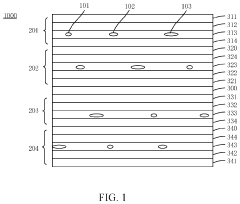
- The method involves forming a confinement structure on a substrate to define wells for precise deposition of active OLED material, creating a non-planar topography with a substantially continuous layer that spans the well boundaries, ensuring uniform thickness and minimizing edge non-uniformities, and using larger confinement wells to span multiple subpixels, thereby increasing the fill factor and reducing manufacturing errors.
Organic light-emitting diode display panel
PatentActiveUS12004399B2
Innovation
- The use of four OLED display panels stacked sequentially with optical adhesive layers and transparent anode layers, allowing for increased screen resolution without the need for fine metal masks or increased array layer density, as subpixels emit light in the same direction without overlapping.
Power Efficiency vs Resolution Trade-offs
The optimization of OLED displays presents a fundamental challenge in balancing power efficiency against resolution requirements. As pixel density increases to achieve higher resolution displays, power consumption typically rises due to the increased number of pixels that require individual driving. This relationship creates a critical trade-off that manufacturers must navigate when designing high-resolution OLED screens.
At the hardware level, higher pixel densities necessitate smaller individual pixels, which often operate at lower efficiency compared to larger pixels. This efficiency reduction occurs because smaller OLED pixels require higher current densities to achieve the same brightness levels as larger pixels, resulting in proportionally greater power consumption. Industry measurements indicate that doubling pixel density can increase power requirements by 30-45% when maintaining equivalent brightness levels.
The power-resolution relationship is further complicated by the subpixel architecture employed. Traditional RGB stripe configurations consume more power than PenTile arrangements at equivalent resolutions, as the latter uses fewer subpixels. However, this power advantage comes at the cost of potential color accuracy and text rendering quality, particularly noticeable in high-contrast scenarios.
Display driving techniques significantly impact this trade-off. Variable refresh rate technologies can reduce power consumption by up to 20% in high-resolution displays by adjusting refresh frequencies based on content requirements. Similarly, pixel-level dimming algorithms that selectively reduce brightness in less critical screen areas can achieve 15-30% power savings while maintaining perceived resolution quality.
Content-adaptive resolution switching represents another promising approach. By dynamically adjusting effective resolution based on content type and viewing distance, modern OLED displays can achieve optimal power efficiency without compromising user experience. Studies show that users typically cannot distinguish between native and slightly downscaled resolutions during motion-heavy content, allowing for strategic power conservation during these periods.
The industry has begun exploring advanced compensation circuits that improve power efficiency at higher resolutions. These circuits optimize voltage delivery to individual pixels based on content characteristics, potentially reducing power requirements by 10-25% compared to conventional driving methods. Such innovations help flatten the traditionally steep power-resolution curve, making higher pixel densities more commercially viable.
Manufacturing Yield Challenges
Manufacturing yield challenges represent a critical bottleneck in the optimization of OLED pixel density for high-resolution screens. As pixel density increases, the manufacturing complexity grows exponentially, leading to significant yield reduction in production lines. Current industry standards pushing beyond 600 PPI (pixels per inch) face yield rates that can drop below 70% for premium displays, substantially increasing production costs and limiting market accessibility.
The primary yield challenge stems from the precision requirements of depositing organic materials through fine metal masks (FMM). When pixel sizes decrease below 20 micrometers, mask alignment becomes extraordinarily difficult, with tolerance requirements in the sub-micron range. Even minor deviations in alignment can cause color mixing between adjacent sub-pixels, resulting in visible defects and color inaccuracies that render entire panels unusable.
Thermal management during the deposition process presents another significant yield challenge. Higher pixel densities create more concentrated heat zones that can cause uneven material deposition and premature degradation of organic compounds. Manufacturing facilities must maintain temperature variations within ±0.5°C across large substrates, a requirement that becomes increasingly difficult as panel sizes grow while pixel dimensions shrink.
Material purity requirements also intensify with higher pixel densities. Contaminants that might be tolerable in lower-resolution displays can cause catastrophic pixel failures in high-density screens. Current manufacturing environments require cleanroom conditions exceeding Class 10 (ISO 4) standards, with material purity levels above 99.999% for key organic compounds.
Electrical defects represent another yield-limiting factor. As pixel circuits become more densely packed, the probability of short circuits and open circuits increases dramatically. The thin-film transistor (TFT) backplanes that drive OLED pixels must maintain exceptional uniformity across millions of transistors, with threshold voltage variations kept below 100mV to ensure consistent brightness across the display.
Industry leaders are exploring several approaches to address these yield challenges, including inkjet printing technologies that eliminate the need for fine metal masks, laser-assisted patterning methods that improve deposition precision, and AI-powered defect detection systems that can identify potential failures earlier in the production process. However, each solution introduces its own set of manufacturing complexities that must be balanced against the benefits of increased pixel density.
Unlock deeper insights with Patsnap Eureka Quick Research — get a full tech report to explore trends and direct your research. Try now!
Generate Your Research Report Instantly with AI Agent
Supercharge your innovation with Patsnap Eureka AI Agent Platform!