Integration Strategies With Standard SMD Components For Hybrid Builds
SEP 1, 20259 MIN READ
Generate Your Research Report Instantly with AI Agent
Patsnap Eureka helps you evaluate technical feasibility & market potential.
Hybrid Integration Background and Objectives
Hybrid integration technology represents the convergence of different electronic component mounting and interconnection methodologies, primarily combining Surface Mount Technology (SMT) with other assembly techniques. This technological approach has evolved significantly over the past three decades, transitioning from experimental implementations to standardized manufacturing processes that are now essential in modern electronics production.
The evolution of hybrid integration began in the late 1980s when traditional through-hole technology started giving way to surface mount technology. During this transition period, manufacturers faced significant challenges in accommodating both technologies simultaneously. By the early 2000s, the industry had developed more sophisticated approaches to hybrid integration, particularly as miniaturization demands increased and new component types emerged.
Today's hybrid integration strategies focus on optimizing the coexistence of standard Surface Mount Device (SMD) components with specialized elements such as chip-on-board assemblies, flexible circuits, and three-dimensional packaging solutions. This integration has become increasingly important as electronic devices continue to demand higher functionality in smaller form factors.
The primary objective of hybrid integration is to maximize the benefits of established SMD manufacturing processes while incorporating specialized components that may require different mounting techniques. This approach aims to achieve optimal performance, reliability, and cost-effectiveness in electronic assemblies without sacrificing production efficiency or scalability.
Current technological trends in hybrid integration include the development of advanced substrate materials that can accommodate diverse component types, improved thermal management solutions for heterogeneous assemblies, and automated manufacturing processes capable of handling multiple component technologies in a single production line.
The market drivers behind hybrid integration strategies include the growing demand for wearable electronics, Internet of Things (IoT) devices, advanced medical implants, and automotive electronics—all of which require combinations of standard components with specialized elements in compact form factors.
Technical objectives for advancing hybrid integration include developing standardized design methodologies that account for the electrical, mechanical, and thermal interactions between different component types; creating more versatile manufacturing equipment capable of handling diverse assembly requirements; and establishing robust quality assurance protocols for heterogeneous electronic assemblies.
As the electronics industry continues to push boundaries in terms of functionality, size, and performance, hybrid integration strategies with standard SMD components will play an increasingly critical role in enabling next-generation electronic products across multiple sectors.
Market Analysis for Hybrid SMD Assembly Solutions
The hybrid SMD assembly market is experiencing significant growth, driven by the increasing demand for miniaturized electronic devices with enhanced functionality. Current market valuations indicate that the global hybrid assembly solutions sector reached approximately 5.7 billion USD in 2022, with projections suggesting a compound annual growth rate of 7.3% through 2028. This growth trajectory is primarily fueled by the telecommunications, automotive, and consumer electronics industries, which collectively account for over 65% of the total market share.
Consumer electronics remains the dominant application segment, representing nearly 38% of the hybrid SMD assembly market. This dominance stems from the continuous evolution of smartphones, wearables, and IoT devices that require increasingly complex integration of standard SMD components with advanced packaging technologies. The automotive sector follows closely, showing the fastest growth rate at 9.2% annually, as vehicles incorporate more sophisticated electronic systems for safety, connectivity, and autonomous driving capabilities.
Geographically, Asia-Pacific leads the market with approximately 45% share, attributed to the strong presence of electronic manufacturing services (EMS) providers in China, Taiwan, South Korea, and Japan. North America and Europe follow with 27% and 21% market shares respectively, with particular strength in high-reliability applications for aerospace, defense, and medical devices.
The market landscape reveals a clear trend toward flexible manufacturing solutions that can accommodate both traditional SMD components and advanced packaging technologies. End-users are increasingly demanding assembly solutions that offer scalability, reduced time-to-market, and cost efficiency while maintaining high reliability standards. This has created a growing market segment for hybrid assembly equipment that can handle multiple component types and packaging technologies in a single production line.
Industry surveys indicate that manufacturers are willing to invest 15-20% more in hybrid assembly solutions compared to traditional SMD-only equipment, recognizing the long-term cost benefits and production flexibility these systems provide. The return on investment period for such systems has decreased from 3-4 years to approximately 18-24 months, further accelerating market adoption.
Contract manufacturers report that clients are increasingly specifying hybrid assembly capabilities in their manufacturing partner requirements, with 72% of new manufacturing contracts including provisions for mixed technology assembly. This trend underscores the strategic importance of hybrid assembly capabilities in maintaining competitiveness in the electronics manufacturing landscape.
Current Challenges in Hybrid SMD Integration
Despite significant advancements in hybrid electronics manufacturing, several critical challenges persist when integrating standard Surface Mount Device (SMD) components into hybrid builds. The primary obstacle remains the fundamental incompatibility between traditional rigid PCB manufacturing processes and flexible or non-planar substrate requirements. This creates significant thermal management issues, as standard SMD components designed for conventional PCBs often experience thermal stress when mounted on flexible substrates with different thermal expansion coefficients.
Dimensional tolerance discrepancies present another major hurdle. Standard SMD components typically require precise placement with tolerances of ±0.1mm or better, which becomes increasingly difficult to maintain on flexible or curved surfaces. This challenge is compounded by the dynamic nature of flexible substrates, where mechanical deformation during operation can stress solder joints and component connections, leading to premature failures.
Adhesion reliability between SMD components and non-traditional substrates remains problematic. Conventional solder processes may not provide adequate mechanical strength on polymer or textile substrates, necessitating alternative bonding methods that often lack the established reliability data of traditional soldering techniques. This uncertainty increases risk in product development cycles.
The manufacturing equipment ecosystem presents additional barriers. Most pick-and-place machines and reflow ovens are optimized for flat, rigid PCBs, requiring significant modifications or specialized equipment for hybrid builds. This increases production costs and limits scalability for mass manufacturing scenarios.
Testing and quality assurance methodologies also lag behind manufacturing capabilities. Standard electrical testing procedures designed for rigid PCBs often cannot adequately assess connections on flexible or conformable substrates, creating verification gaps in production processes.
Regulatory compliance adds another layer of complexity. Many hybrid electronic applications target wearable or medical markets with stringent safety requirements, yet existing standards primarily address conventional electronics manufacturing. This regulatory uncertainty can extend development timelines and increase compliance costs.
Material compatibility issues further complicate integration efforts. Chemical interactions between flexible substrate materials and standard SMD component packaging or soldering materials can lead to degradation over time, particularly in harsh environmental conditions. This necessitates extensive reliability testing that traditional electronics may not require.
These multifaceted challenges collectively create significant barriers to widespread adoption of hybrid electronics solutions, despite their compelling advantages in form factor and application versatility.
Current Hybrid SMD Integration Methodologies
01 PCB design optimization for SMD integration
Optimizing printed circuit board (PCB) design is crucial for efficient integration of standard surface-mount device (SMD) components. This includes strategic placement of components to minimize trace lengths, reduce electromagnetic interference, and improve thermal management. Advanced PCB layout techniques can significantly enhance the overall integration efficiency by allowing for higher component density while maintaining signal integrity and manufacturability.- PCB design optimization for SMD integration: Optimizing printed circuit board (PCB) design is crucial for efficient integration of standard surface-mount device (SMD) components. This includes strategic placement of components to minimize trace lengths, reduce electromagnetic interference, and improve thermal management. Advanced PCB layout techniques can significantly enhance the overall integration efficiency by allowing for higher component density while maintaining signal integrity and manufacturability.
- Automated assembly techniques for SMD components: Automated assembly methods significantly improve the integration efficiency of standard SMD components. These techniques include pick-and-place automation, reflow soldering optimization, and machine vision inspection systems. By implementing standardized assembly processes with precise component handling and placement, manufacturers can achieve higher throughput, reduced defect rates, and improved consistency in electronic device production.
- Miniaturization and packaging innovations: Advanced packaging technologies enable more efficient integration of standard SMD components. These innovations include chip-scale packaging, multi-chip modules, and 3D stacking techniques that maximize space utilization while maintaining or improving electrical performance. By reducing the footprint of individual components and optimizing their arrangement, these approaches allow for higher functional density in electronic devices without compromising reliability.
- Thermal management solutions for dense SMD integration: Effective thermal management is essential for high-density SMD component integration. Strategies include the use of thermal vias, heat spreaders, and advanced cooling techniques to dissipate heat efficiently from densely packed components. Proper thermal design ensures optimal operating temperatures, prevents thermal-related failures, and extends the lifespan of electronic devices while allowing for more compact integration of standard SMD components.
- Standardization and modular design approaches: Standardization of component footprints, interfaces, and assembly processes enables more efficient integration of SMD components. Modular design approaches allow for reusable circuit blocks that can be easily integrated into various products. By establishing consistent design rules and component libraries, engineers can accelerate development cycles, improve manufacturing yields, and enhance the scalability of electronic designs while maintaining compatibility with standard SMD components.
02 Automated assembly techniques for SMD components
Automated assembly methods significantly improve the integration efficiency of standard SMD components. These techniques include pick-and-place machines, reflow soldering processes, and automated optical inspection systems that ensure accurate placement and reliable connections. The automation of these processes reduces human error, increases throughput, and enables consistent quality in high-volume production environments.Expand Specific Solutions03 Miniaturization and packaging innovations
Innovations in component packaging and miniaturization techniques enable more efficient integration of standard SMD components. These include advanced package designs like quad flat no-leads (QFN), ball grid arrays (BGA), and chip-scale packages (CSP) that reduce footprint while maintaining or improving electrical performance. These packaging innovations allow for higher component density and better utilization of board space.Expand Specific Solutions04 Thermal management solutions for SMD integration
Effective thermal management is essential for reliable integration of SMD components, especially in high-density applications. Solutions include thermal vias, heat spreaders, and optimized component placement to facilitate heat dissipation. Advanced cooling techniques such as integrated heat sinks and thermal interface materials help maintain optimal operating temperatures, preventing thermal-related failures and extending component lifespan.Expand Specific Solutions05 Modular design approaches for flexible integration
Modular design approaches enhance the flexibility and efficiency of integrating standard SMD components. By dividing complex systems into functional modules with standardized interfaces, designers can simplify testing, maintenance, and upgrades. This approach allows for parallel development of different system sections, reuse of proven designs, and easier troubleshooting, ultimately reducing time-to-market and improving overall integration efficiency.Expand Specific Solutions
Leading Manufacturers and Industry Ecosystem
The integration of standard SMD components for hybrid builds is currently in a growth phase, with the market expanding rapidly due to increasing demand for miniaturized, high-performance electronic systems. The global market size is estimated to exceed $15 billion, driven by applications in consumer electronics, automotive, and medical devices. From a technological maturity perspective, industry leaders like Intel, Samsung Electronics, and Taiwan Semiconductor Manufacturing Co. have established advanced integration capabilities, while companies such as Qualcomm, Texas Instruments, and Infineon Technologies are focusing on specialized hybrid solutions. Applied Materials and GlobalFoundries are developing manufacturing processes that bridge traditional SMD technology with emerging integration methods. The competitive landscape shows a clear division between semiconductor giants with comprehensive solutions and specialized players focusing on niche applications.
Intel Corp.
Technical Solution: Intel has developed advanced integration strategies for hybrid builds combining standard SMD components with their silicon technologies. Their Embedded Multi-die Interconnect Bridge (EMIB) technology enables high-density connections between heterogeneous chips without the need for silicon interposers. This approach allows for the integration of standard SMD components alongside specialized silicon in a cost-effective manner. Intel's Foveros 3D packaging technology further extends these capabilities by enabling vertical stacking of logic chips with different process nodes and SMD components. Their recent advancements include the Co-EMIB architecture that combines both horizontal and vertical integration methods, allowing for complex hybrid systems that incorporate standard off-the-shelf SMD components with custom silicon solutions. Intel has also developed specialized solder materials and reflow profiles optimized for mixed component assemblies to address thermal expansion mismatches between different component types.
Strengths: Superior interconnect density and bandwidth between heterogeneous components; reduced signal path lengths improving electrical performance; modular design approach enabling mix-and-match of components. Weaknesses: Higher manufacturing complexity requiring specialized equipment; thermal management challenges in densely packed hybrid assemblies; potential reliability concerns at interconnect points between different component technologies.
Samsung Electronics Co., Ltd.
Technical Solution: Samsung has developed advanced integration strategies for hybrid builds through their Multi-Chip Package (MCP) technology platform. Their approach utilizes advanced substrate technologies including High-Density Interconnect (HDI) and Embedded Component Packaging (ECP) to achieve miniaturization while maintaining compatibility with standard SMD assembly processes. Samsung's Package-on-Package (PoP) technology demonstrates this hybrid approach by stacking memory packages on top of processor packages with standardized interfaces, allowing for the integration of different component types manufactured using different process technologies. For mobile applications, Samsung has pioneered their integrated passive device (IPD) technology that embeds passive components within the substrate while allowing standard SMD components to be mounted on the surface. Their recent Fan-Out Wafer Level Packaging (FOWLP) technology further advances hybrid integration by redistributing I/O connections to accommodate standard SMD component pitches while maintaining the performance benefits of wafer-level packaging. Samsung has also developed specialized material systems that address the thermal expansion mismatch between different component types in hybrid assemblies.
Strengths: Industry-leading miniaturization capabilities; excellent high-frequency performance in RF applications; established high-volume manufacturing infrastructure. Weaknesses: Higher component cost for specialized packages; complex supply chain management; thermal challenges in densely packed mobile applications.
Key Technical Innovations in Hybrid Assembly
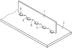
SMD-capable hybrid circuit
PatentWO1999051071A1
Innovation
- The hybrid circuit features connection surfaces extending to the lower edge for direct SMD soldering, with recessed solder pads providing additional solder volume for durable joints and optional anti-tilt elements for enhanced stability, allowing for vertical surface mounting and efficient reflow soldering processes.
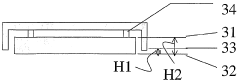
Method for assembling at least one substrate-integrating component by surface mounting, a corresponding support and component
PatentWO2005020647A2
Innovation
- A method involving a support with recesses and indexing patterns for substrates, allowing simultaneous deposition of solder paste and securement of both surface-mounted and encompassing components through remelting, facilitating rapid and automated assembly without pre-cutting the substrate.
Supply Chain Considerations for Hybrid Builds
Supply chain management represents a critical factor in the successful implementation of hybrid builds that integrate standard SMD components. The complexity of hybrid electronic assemblies demands a robust and resilient supply chain strategy that addresses multiple dimensions of component sourcing, inventory management, and production planning.
Component availability presents the foremost challenge in hybrid build supply chains. Standard SMD components typically enjoy broader market availability compared to specialized hybrid assembly components. However, manufacturers must establish relationships with multiple suppliers to mitigate risks associated with single-source dependencies. Implementing a multi-tiered supplier qualification program ensures consistent component quality while maintaining supply continuity during market disruptions.
Lead time management requires particular attention in hybrid builds. SMD components generally feature shorter procurement cycles, whereas specialized hybrid assembly materials may involve extended lead times. Effective forecasting models that incorporate historical usage patterns, market trends, and project pipelines can optimize inventory levels. Just-in-time procurement strategies must be balanced with strategic buffer stocks for critical components with volatile supply conditions.
Cost optimization presents another significant consideration. The integration of standard SMD components into hybrid builds offers potential economies of scale, yet requires careful analysis of total acquisition costs. Beyond unit pricing, manufacturers must evaluate handling requirements, storage conditions, and potential obsolescence risks. Component standardization across product lines can enhance purchasing power while reducing inventory complexity.
Quality assurance throughout the supply chain demands rigorous protocols. Supplier certification programs should verify compliance with industry standards such as IPC-A-610 for electronic assemblies. Incoming inspection procedures must address the unique characteristics of components intended for hybrid integration, with particular attention to moisture sensitivity, solderability, and dimensional stability.
Logistics considerations for hybrid builds extend beyond traditional electronic assembly requirements. Temperature-controlled transportation and storage may be necessary for certain component types. Packaging specifications must prevent damage from electrostatic discharge while protecting delicate terminations. Traceability systems should maintain comprehensive component history from manufacturer to final assembly.
Regulatory compliance adds another layer of complexity to hybrid build supply chains. Component selection must consider global environmental regulations such as RoHS and REACH, particularly when products target multiple international markets. Documentation requirements for material declarations and compliance certificates necessitate sophisticated data management systems that integrate with supplier portals.
Reliability Testing Standards for Hybrid Assemblies
Reliability testing standards for hybrid assemblies combining standard SMD components with advanced integration techniques have evolved significantly to address the unique challenges of these complex builds. The industry has established comprehensive testing frameworks that evaluate both the individual components and their interactions within the hybrid system.
The primary reliability testing standards include IPC-9701 for thermal cycling reliability, IPC-TM-650 for various mechanical and environmental tests, and MIL-STD-883 for microelectronic devices. These standards have been adapted specifically for hybrid assemblies to account for the different thermal expansion coefficients, material interfaces, and stress points that occur when integrating standard SMD components with advanced substrates or embedding technologies.
Temperature cycling tests represent a critical evaluation method, typically requiring components to withstand between 500-1000 cycles from -40°C to +125°C for consumer applications, and more extreme ranges for automotive or aerospace implementations. The rate of temperature change is carefully controlled to simulate real-world conditions while accelerating potential failure mechanisms.
Mechanical shock and vibration testing follows standards such as JESD22-B104 and IEC 60068, with hybrid assemblies often requiring more rigorous protocols due to the complex interconnection structures. These tests evaluate the integrity of solder joints, wire bonds, and adhesive interfaces under dynamic stress conditions that simulate transportation, handling, and operational environments.
Humidity and moisture sensitivity testing has gained increased importance for hybrid assemblies, particularly when porous substrates or organic materials are incorporated. The J-STD-020 standard classifies components according to their moisture sensitivity levels, with hybrid assemblies often requiring special consideration due to their heterogeneous material composition.
Accelerated life testing methodologies such as Highly Accelerated Life Testing (HALT) and Highly Accelerated Stress Screening (HASS) have been adapted specifically for hybrid assemblies to identify potential failure modes that might not be detected through conventional testing approaches. These methods apply combined stresses (temperature, vibration, electrical) simultaneously to precipitate latent defects.
Electrical performance verification under environmental stress conditions represents another critical aspect of reliability testing for hybrid assemblies. Standards like IEC 61000 series address electromagnetic compatibility concerns, which are particularly relevant when integrating digital and analog components in close proximity within hybrid builds.
The development of specialized test fixtures and methodologies for hybrid assemblies continues to evolve, with increasing focus on non-destructive evaluation techniques such as acoustic microscopy, X-ray inspection, and thermal imaging to detect potential reliability issues before they manifest as functional failures.
Unlock deeper insights with Patsnap Eureka Quick Research — get a full tech report to explore trends and direct your research. Try now!
Generate Your Research Report Instantly with AI Agent
Supercharge your innovation with Patsnap Eureka AI Agent Platform!