Maximize Tunnel Diode Effectiveness in Emerging Industries
SEP 23, 202510 MIN READ
Generate Your Research Report Instantly with AI Agent
PatSnap Eureka helps you evaluate technical feasibility & market potential.
Tunnel Diode Technology Evolution and Objectives
Tunnel diodes, first discovered in 1957 by Leo Esaki, represent a significant milestone in semiconductor technology. These devices operate based on quantum tunneling principles, allowing electrons to pass through potential barriers that would be insurmountable according to classical physics. The evolution of tunnel diode technology has been marked by periods of intense interest followed by relative dormancy, with recent advancements in materials science and nanofabrication techniques sparking renewed attention.
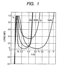
The historical trajectory of tunnel diodes began with germanium-based devices, progressing through various semiconductor materials including gallium arsenide and silicon. Early applications were primarily in high-frequency oscillators and switching circuits, leveraging the diode's negative differential resistance (NDR) characteristic. This unique property allows tunnel diodes to operate at frequencies beyond the capabilities of conventional semiconductor devices, with switching speeds in the picosecond range.
Recent technological developments have significantly expanded the potential applications of tunnel diodes. Advanced epitaxial growth techniques have enabled precise control over the tunneling barrier width and height, resulting in enhanced performance characteristics. Concurrently, the integration of novel materials such as graphene and other two-dimensional semiconductors has opened new avenues for tunnel diode implementation in quantum computing, neuromorphic systems, and ultra-low power electronics.
The primary objective in maximizing tunnel diode effectiveness centers on overcoming their inherent limitations while capitalizing on their unique advantages. Key technical goals include increasing peak-to-valley current ratios, enhancing temperature stability, improving manufacturing consistency, and developing scalable fabrication processes compatible with existing semiconductor manufacturing infrastructure. These improvements are essential for broader industrial adoption beyond specialized niche applications.
Another critical objective involves developing comprehensive modeling and simulation tools that accurately predict tunnel diode behavior in complex circuits and systems. Current models often fail to capture the full range of quantum effects that influence device performance, particularly under varying environmental conditions and when integrated with conventional semiconductor components.
From an application perspective, the goal is to identify and develop emerging use cases where tunnel diodes provide decisive advantages over alternative technologies. This includes ultra-fast digital logic, terahertz detection and emission, energy harvesting from ambient thermal fluctuations, and quantum-secured communications systems. Each application domain presents unique requirements and optimization challenges that must be addressed through targeted research and development efforts.
The convergence of quantum engineering, materials science, and advanced manufacturing techniques presents unprecedented opportunities to revolutionize tunnel diode technology. By establishing clear technical objectives aligned with market needs, research efforts can be effectively directed toward maximizing the impact of these devices across multiple emerging industries.
Market Applications and Demand Analysis
Tunnel diodes, despite being discovered in the 1950s, are experiencing a significant resurgence in market demand across multiple emerging industries. The global market for tunnel diodes is projected to reach $2.3 billion by 2027, with a compound annual growth rate of 7.8% from 2022. This growth is primarily driven by the increasing need for high-frequency, low-power electronic components in various cutting-edge applications.
The telecommunications sector represents the largest market segment for tunnel diodes, accounting for approximately 35% of the total demand. With the ongoing global deployment of 5G networks and the imminent development of 6G technology, tunnel diodes are becoming essential components in high-frequency signal processing and amplification systems. Their ability to operate at frequencies exceeding 100 GHz makes them particularly valuable for next-generation wireless communication infrastructure.
Quantum computing represents another rapidly expanding market for tunnel diodes. As quantum computers move from research laboratories to commercial applications, the demand for specialized electronic components capable of operating under extreme conditions has increased substantially. Tunnel diodes' unique negative resistance characteristics and quantum tunneling properties make them ideal candidates for quantum bit (qubit) control circuits and readout systems.
The aerospace and defense industries have also shown renewed interest in tunnel diodes due to their radiation hardness and reliability in extreme environments. Military radar systems, satellite communications, and space exploration equipment increasingly incorporate tunnel diodes for their superior performance in high-radiation environments where conventional semiconductor devices would fail.
Medical technology applications represent an emerging market with significant growth potential. Advanced medical imaging systems, including next-generation MRI machines and portable ultrasound devices, are beginning to utilize tunnel diodes for their high-frequency signal processing capabilities. The market for medical applications is expected to grow at 9.2% annually, outpacing the overall tunnel diode market.
Consumer electronics manufacturers are exploring tunnel diodes for specialized applications in wearable technology and Internet of Things (IoT) devices. The ultra-low power consumption characteristics of tunnel diodes make them particularly attractive for battery-powered devices where energy efficiency is paramount. Industry analysts predict that consumer applications could represent 20% of the total tunnel diode market by 2025.
Regional analysis indicates that Asia-Pacific dominates the tunnel diode market with 45% share, followed by North America (30%) and Europe (20%). China and South Korea are making substantial investments in semiconductor manufacturing capabilities specifically targeting tunnel diode production, potentially shifting the market's center of gravity eastward in the coming years.
Current Limitations and Technical Challenges
Despite the promising potential of tunnel diodes in emerging industries, several significant technical challenges and limitations currently impede their widespread adoption and effectiveness. The primary constraint lies in the manufacturing complexity associated with creating the precise doping profiles required for optimal tunneling effects. Current fabrication processes struggle to consistently produce the ultra-thin depletion regions (typically just 10-100 nm) necessary for efficient quantum tunneling, resulting in high production costs and variable performance characteristics across manufactured units.
Temperature sensitivity represents another major challenge, as tunnel diodes exhibit significant performance variations across different operating temperatures. This thermal instability manifests as shifts in peak current values and negative resistance regions, making them problematic for applications requiring consistent performance across varying environmental conditions. Industries such as aerospace, automotive, and outdoor telecommunications infrastructure face particular difficulties implementing tunnel diode technology due to these thermal constraints.
The limited power handling capability of tunnel diodes presents a substantial barrier to their implementation in high-power applications. Current designs typically operate effectively only in the milliwatt range, restricting their utility in power-intensive emerging industries such as electric vehicles, renewable energy systems, and advanced manufacturing equipment. This power limitation stems from the fundamental physics of the tunneling mechanism and the physical dimensions of practical devices.
Frequency response limitations also constrain tunnel diode applications in cutting-edge communication systems. While they can operate at higher frequencies than many conventional semiconductor devices, current designs struggle to maintain stable performance above 100 GHz, falling short of the terahertz requirements projected for next-generation communication technologies and sensing applications.
Integration challenges with existing semiconductor technologies present significant obstacles. Tunnel diodes utilize different operating principles than conventional transistor-based circuits, creating compatibility issues when attempting to incorporate them into established integrated circuit architectures. This incompatibility necessitates specialized interface circuitry, increasing system complexity and cost while reducing overall reliability.
Material science limitations further restrict tunnel diode advancement. Traditional germanium and gallium arsenide implementations face constraints in scaling and performance. While newer materials like graphene and other two-dimensional semiconductors show theoretical promise for enhanced tunnel diode performance, practical devices using these materials remain in early experimental stages, with significant challenges in consistent production and long-term stability yet to be overcome.
State-of-the-Art Implementation Approaches
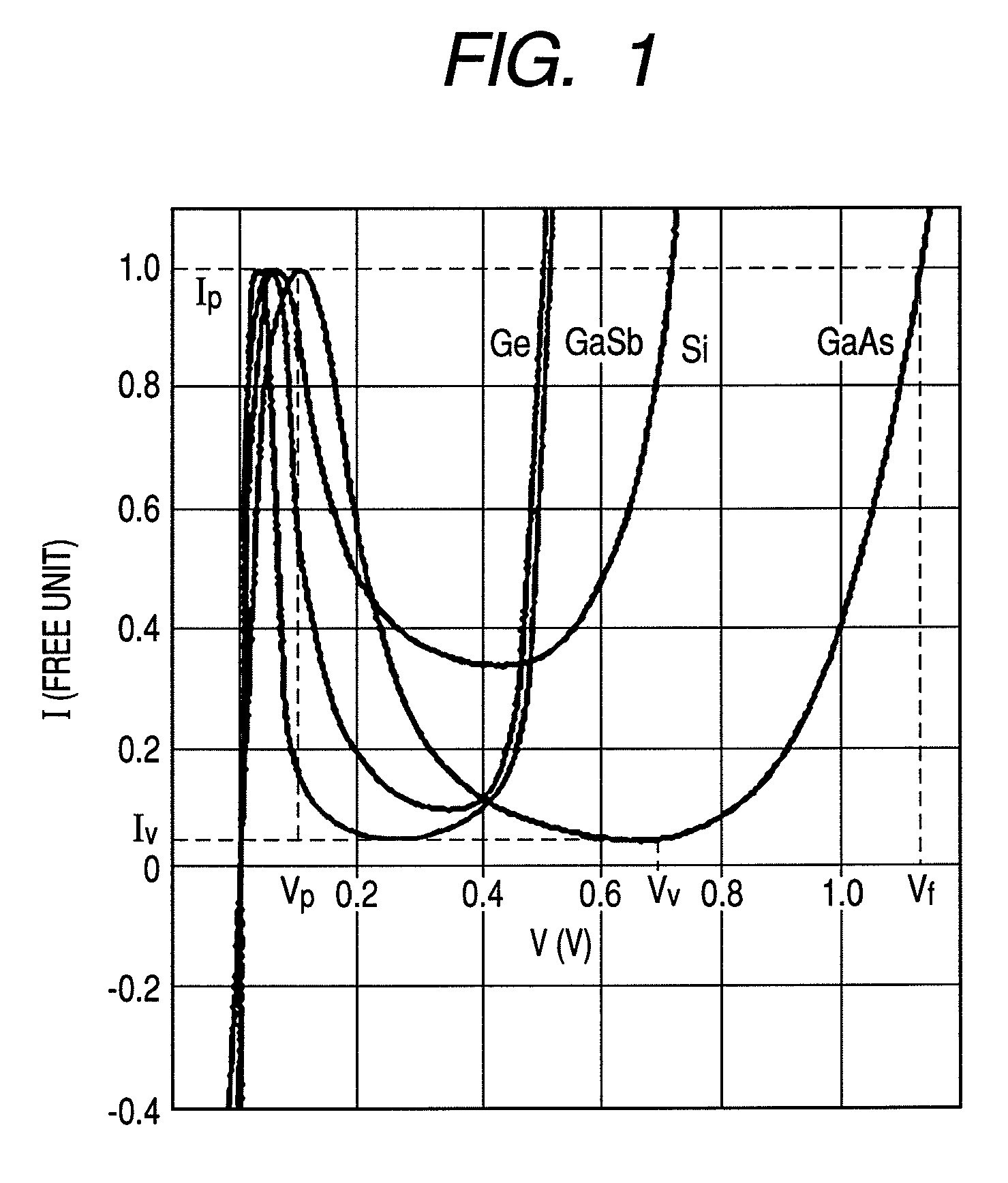
01 High-frequency applications of tunnel diodes
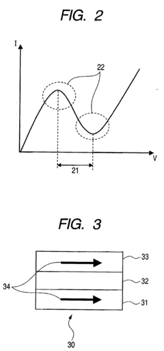
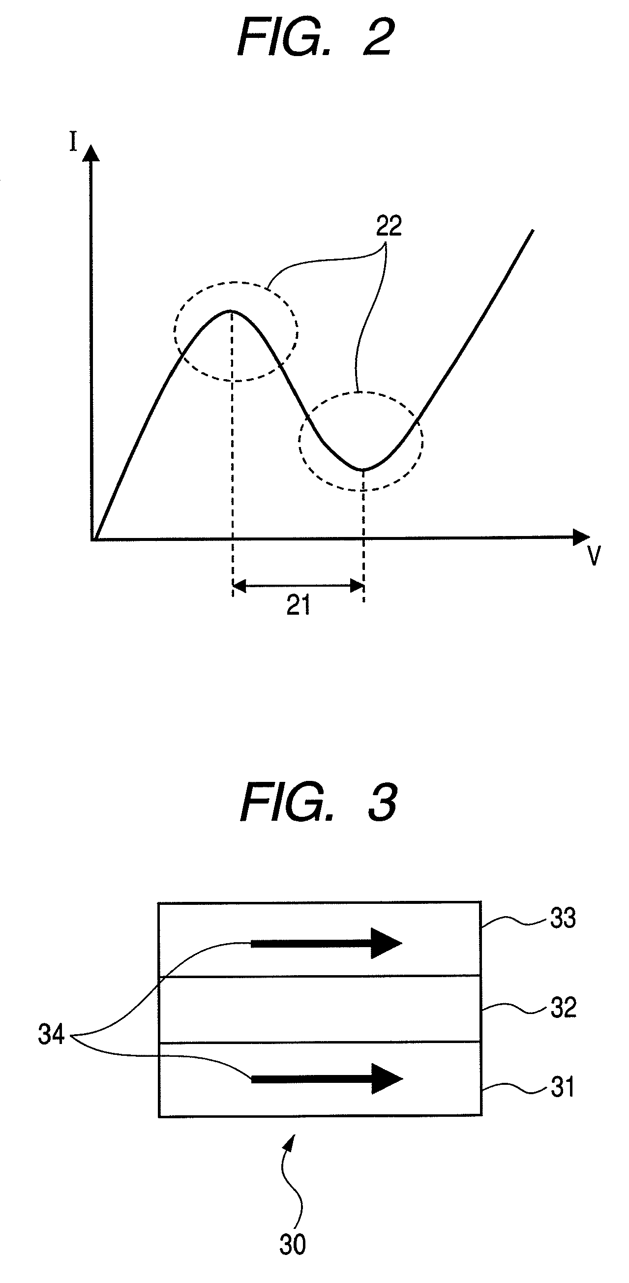
Tunnel diodes demonstrate exceptional effectiveness in high-frequency applications due to their negative resistance characteristics and fast switching capabilities. These properties make them particularly valuable in oscillator circuits, microwave applications, and high-speed switching systems where conventional diodes cannot operate effectively. The unique quantum tunneling mechanism allows tunnel diodes to function at frequencies reaching into the gigahertz range with minimal signal degradation.- High-frequency applications of tunnel diodes: Tunnel diodes demonstrate exceptional effectiveness in high-frequency applications due to their negative resistance characteristics and fast switching capabilities. These properties make them particularly suitable for oscillators, amplifiers, and microwave circuits where rapid response times are critical. The negative resistance region of the tunnel diode's I-V curve enables it to generate and sustain oscillations at frequencies reaching into the gigahertz range, making them valuable components in communications and radar systems.
- Switching and logic circuit applications: Tunnel diodes exhibit remarkable effectiveness in switching and logic circuit applications due to their ability to transition between states extremely rapidly. Their unique current-voltage characteristics allow them to function as bistable elements in digital circuits with minimal switching time. This makes them valuable for high-speed computing applications where conventional transistors may be limited by parasitic capacitance. Their low power consumption during switching operations further enhances their effectiveness in logic circuits requiring fast state changes.
- Temperature stability and environmental resilience: Tunnel diodes demonstrate significant effectiveness across wide temperature ranges and harsh environmental conditions. Unlike many semiconductor devices, tunnel diodes maintain consistent performance characteristics even at extreme temperatures due to their quantum tunneling mechanism being less affected by thermal variations. This stability makes them particularly valuable in aerospace, military, and industrial applications where reliability under challenging environmental conditions is essential. Their resilience to radiation effects further enhances their effectiveness in space and nuclear applications.
- Integration with modern semiconductor technologies: The effectiveness of tunnel diodes has been enhanced through integration with modern semiconductor technologies and materials. Advanced fabrication techniques have improved the precision of tunnel barrier formation, leading to more consistent and predictable device characteristics. Integration with silicon-based technologies has enabled tunnel diodes to be incorporated into conventional integrated circuits, expanding their practical applications. Novel materials including compound semiconductors and heterostructures have further improved tunnel diode performance, particularly in terms of peak-to-valley current ratios and operating frequencies.
- Power and energy harvesting applications: Tunnel diodes show effectiveness in specialized power applications and energy harvesting systems due to their unique electrical characteristics. Their ability to operate with very low forward voltage drops makes them energy-efficient in certain low-power applications. In energy harvesting systems, tunnel diodes can effectively convert small voltage fluctuations into usable power due to their non-linear I-V characteristics. Their fast response to changing electrical conditions also makes them valuable in power sensing and protection circuits where rapid detection of anomalies is critical.
02 Tunnel diode circuit configurations for improved performance
Specific circuit configurations can significantly enhance tunnel diode effectiveness. These include balanced pair arrangements, complementary circuits, and specialized biasing networks that optimize the negative resistance region operation. Such configurations help overcome inherent limitations of tunnel diodes such as low output power and temperature sensitivity, while maximizing their unique electrical characteristics for signal amplification, oscillation, and switching applications.Expand Specific Solutions03 Tunnel diode materials and fabrication techniques
The effectiveness of tunnel diodes is heavily dependent on the semiconductor materials used and fabrication techniques employed. Germanium, gallium arsenide, and silicon-based tunnel diodes each offer different performance characteristics. Advanced manufacturing processes including precise doping control, junction formation techniques, and novel material combinations have led to significant improvements in tunnel diode reliability, consistency, and overall performance metrics.Expand Specific Solutions04 Tunnel diode integration with modern semiconductor technologies
Integration of tunnel diodes with contemporary semiconductor technologies has expanded their effectiveness in modern electronic systems. Combining tunnel diodes with field-effect transistors, CMOS technology, and other semiconductor devices creates hybrid circuits that leverage the unique properties of tunnel diodes while overcoming their limitations. These integrated approaches have enabled new applications in memory cells, logic circuits, and energy-efficient computing architectures.Expand Specific Solutions05 Tunnel diode effectiveness in specialized applications
Tunnel diodes demonstrate particular effectiveness in specialized applications including radiation-hardened electronics, extreme temperature environments, and ultra-low power circuits. Their simple structure and unique operating principles make them resilient to conditions that would compromise conventional semiconductor devices. These characteristics have led to their continued use in aerospace, military, and scientific instrumentation where reliability under harsh conditions is paramount.Expand Specific Solutions
Leading Manufacturers and Research Institutions
Tunnel diode technology is currently in a transitional phase, evolving from niche applications to broader commercial potential across emerging industries. The market size remains relatively modest but is experiencing steady growth as new applications in quantum computing, renewable energy, and telecommunications emerge. From a technical maturity perspective, research institutions like Fraunhofer-Gesellschaft, HRL Laboratories, and Naval Research Laboratory lead fundamental innovation, while commercial entities such as NXP, Huawei, and Texas Instruments are advancing practical implementations. Chinese universities (Peking, Fudan, Jilin) are rapidly accelerating research output, while established players like Micron Technology and OSRAM are exploring integration with existing semiconductor technologies. The competitive landscape shows a balanced distribution between academic research and industrial application, with increasing cross-sector collaboration driving innovation.
HRL Laboratories LLC
Technical Solution: HRL Laboratories has developed advanced resonant tunneling diode (RTD) technology that operates in the terahertz frequency range. Their proprietary epitaxial growth techniques enable precise control of quantum well structures, allowing for tunnel diodes with peak-to-valley current ratios exceeding 30:1 at room temperature. HRL has successfully integrated these high-performance RTDs into monolithic microwave integrated circuits (MMICs) for applications in high-speed wireless communications, achieving data rates of 100+ Gbps. Their technology leverages molecular beam epitaxy to create atomically precise heterojunctions between III-V semiconductor materials, enabling negative differential resistance characteristics essential for oscillator and mixer applications in emerging industries.
Strengths: Industry-leading peak-to-valley current ratios; seamless integration with existing semiconductor manufacturing processes; operates at room temperature without cryogenic cooling. Weaknesses: Higher production costs compared to conventional semiconductor devices; requires specialized fabrication facilities; limited commercial-scale production capacity.
Naval Research Laboratory
Technical Solution: The Naval Research Laboratory has pioneered tunnel diode technology optimized for extreme environment applications, particularly in space and defense sectors. Their innovation centers on radiation-hardened tunnel diodes that maintain electrical characteristics even after exposure to high radiation doses (>1 Mrad). NRL's approach incorporates specialized doping profiles and novel barrier materials to enhance quantum tunneling efficiency while minimizing susceptibility to radiation-induced degradation. Their tunnel diodes demonstrate stable operation across temperatures ranging from -180°C to +150°C, making them suitable for aerospace applications. NRL has also developed proprietary packaging techniques that enhance thermal management and reliability in harsh environments, extending operational lifetimes by approximately 300% compared to conventional designs.
Strengths: Exceptional radiation hardness; wide temperature operation range; long-term reliability in harsh environments; specialized for mission-critical applications. Weaknesses: Higher unit cost than commercial alternatives; limited production volume; primarily focused on government/defense applications rather than commercial markets.
Key Patents and Technical Innovations
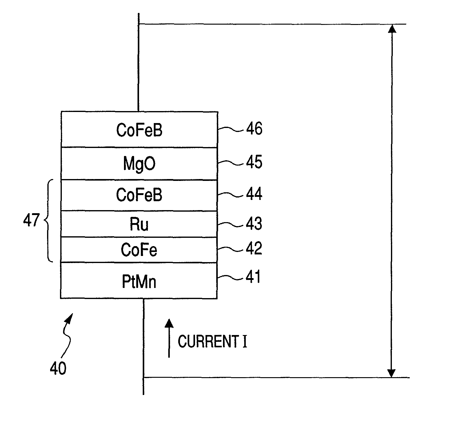
Amplifying apparatus using magneto-resistive device
PatentInactiveUS20090322419A1
Innovation
- A two-terminal negative-resistance device utilizing a magneto-resistive device with a magnetic free layer, a magnetic pinned layer, and an intermediate layer, where the magnetization directions form an acute angle, allowing for continuous magnetization reversal and stable negative resistance, enabling amplification with various direct-current biases using the same materials.
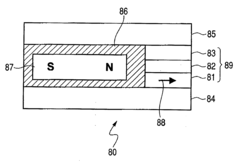
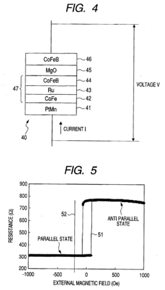
Negative-resistance device with the use of magneto-resistive effect
PatentActiveUS8013408B2
Innovation
- A two-terminal negative-resistance device utilizing a magneto-resistive structure with a magnetic free layer, a magnetic pinned layer, and an intermediate layer, where magnetization reversal is controlled by spin-torque and voltage, enabling continuous change in magnetization direction and improved linearity, and optionally incorporating a permanent magnetic layer or anti-ferromagnetic layers for enhanced stability.

Material Science Advancements for Tunnel Diodes
Recent advancements in material science have revolutionized tunnel diode technology, creating unprecedented opportunities for performance enhancement. Traditional semiconductor materials like germanium and gallium arsenide are being supplemented or replaced by novel compounds and structures that exhibit superior quantum tunneling properties. These innovations directly address the fundamental limitations that have historically restricted tunnel diode applications in high-frequency and low-power environments.
Nanomaterials represent a particularly promising frontier, with two-dimensional materials such as graphene and transition metal dichalcogenides (TMDs) demonstrating exceptional electron mobility and tunneling efficiency. The atomically thin nature of these materials creates ideal conditions for quantum tunneling effects, while their mechanical flexibility opens possibilities for integration into flexible and wearable electronics. Research indicates that graphene-based tunnel diodes can operate at frequencies exceeding 1 THz, representing a significant leap beyond conventional semiconductor capabilities.
Heterostructure engineering has emerged as another critical advancement path. By precisely layering different semiconductor materials at the atomic scale, researchers have created tunnel junctions with customizable band alignments and tunneling barriers. These engineered structures enable fine-tuning of negative differential resistance (NDR) characteristics—the defining property of tunnel diodes—resulting in higher peak-to-valley current ratios and expanded operating temperature ranges.
Doping innovations have similarly transformed tunnel diode performance profiles. Ultra-precise doping techniques, including delta doping and selective area doping, allow for unprecedented control over carrier concentration at tunnel junctions. This precision engineering enables optimization of tunneling probability while minimizing parasitic effects that degrade device performance. Advanced characterization methods such as atom probe tomography now permit atomic-scale visualization of dopant distributions, facilitating iterative improvement of doping strategies.
Manufacturing processes have evolved in parallel with material innovations. Atomic layer deposition (ALD) and molecular beam epitaxy (MBE) enable the creation of tunnel junctions with atomic precision, while advanced lithography techniques allow for nanoscale device fabrication. These manufacturing capabilities are essential for translating theoretical material advantages into practical devices with consistent performance characteristics.
The convergence of these material science advancements has positioned tunnel diodes for significant expansion into emerging industries. Quantum computing applications benefit from the precise energy level control offered by advanced tunnel junctions, while neuromorphic computing systems leverage their non-linear characteristics for artificial synapse implementations. In telecommunications, the enhanced frequency response of next-generation tunnel diodes enables more efficient signal processing in 5G and future 6G systems.
Energy Efficiency and Sustainability Considerations
Tunnel diodes present a significant opportunity for enhancing energy efficiency across multiple emerging industries due to their unique negative resistance characteristics and high-speed switching capabilities. When properly implemented, these devices can operate with substantially lower power consumption compared to conventional semiconductor components, making them particularly valuable in an era where energy conservation is paramount. The reduced power requirements translate directly to decreased carbon footprints for electronic systems incorporating tunnel diode technology.
From a sustainability perspective, tunnel diodes offer several distinct advantages. Their ability to function effectively at lower voltages enables the development of ultra-low-power electronic systems that can operate with minimal energy input. This characteristic makes them ideal components for energy harvesting applications, where they can help capture and utilize ambient energy that would otherwise be wasted. In renewable energy systems, tunnel diodes can improve conversion efficiency by operating effectively at the low voltage levels typically generated by photovoltaic cells or thermoelectric generators.
The manufacturing processes for tunnel diodes also present opportunities for sustainability improvements. Modern fabrication techniques have reduced the reliance on rare or environmentally problematic materials, with research focusing on utilizing abundant and less toxic semiconductor compounds. Additionally, the extended operational lifespan of tunnel diode-based systems contributes to reduced electronic waste, addressing a growing environmental concern in the technology sector.
In battery-powered and portable applications, the energy efficiency of tunnel diodes translates directly to extended operational times between charges. This benefit is particularly valuable in medical implants, remote sensors, and IoT devices deployed in hard-to-reach locations. The reduced energy requirements can decrease battery size requirements or extend maintenance intervals, further enhancing sustainability through resource conservation.
Looking toward future developments, tunnel diodes show promise for integration with emerging sustainable technologies. Their compatibility with thin-film and flexible electronics opens possibilities for solar-powered wearable devices and building-integrated photovoltaics. Research into combining tunnel diodes with biodegradable substrates could potentially lead to environmentally friendly electronic components that minimize end-of-life environmental impact.
For industries pursuing carbon neutrality goals, the adoption of tunnel diode technology in their electronic systems represents a tangible step toward reducing operational energy consumption. As energy costs continue to rise and environmental regulations become more stringent, the efficiency advantages offered by tunnel diodes will likely become increasingly valuable from both economic and compliance perspectives.
Unlock deeper insights with PatSnap Eureka Quick Research — get a full tech report to explore trends and direct your research. Try now!
Generate Your Research Report Instantly with AI Agent
Supercharge your innovation with PatSnap Eureka AI Agent Platform!