

Realize Tunnel Diode Potential in Future-Oriented Projects
SEP 23, 202510 MIN READ
Generate Your Research Report Instantly with AI Agent
PatSnap Eureka helps you evaluate technical feasibility & market potential.
Tunnel Diode Technology Evolution and Objectives
Tunnel diodes, first discovered in 1957 by Leo Esaki, represent a significant milestone in semiconductor technology. These devices operate based on quantum mechanical tunneling, allowing electrons to pass through potential barriers rather than overcoming them. This unique property enables tunnel diodes to function at extremely high frequencies with minimal noise, positioning them as potentially revolutionary components in various electronic applications.
The evolution of tunnel diode technology has progressed through several distinct phases. Initially, germanium-based tunnel diodes dominated the landscape in the late 1950s and early 1960s. However, their adoption was limited by manufacturing challenges and the concurrent rise of transistor technology. The second phase, spanning the 1970s through 1990s, saw tunnel diodes relegated primarily to specialized applications in microwave oscillators and detectors, while mainstream electronics embraced silicon-based integrated circuits.
Recent advancements in materials science and nanofabrication techniques have sparked renewed interest in tunnel diodes. The emergence of III-V semiconductor compounds, graphene, and other two-dimensional materials has significantly enhanced the performance characteristics of modern tunnel diodes. These improvements include higher peak-to-valley current ratios, increased operating frequencies reaching into the terahertz range, and greater temperature stability.
The primary technical objective for tunnel diode development centers on overcoming historical limitations while capitalizing on their inherent advantages. Key goals include improving manufacturing scalability to enable cost-effective mass production, enhancing integration compatibility with conventional CMOS technology, and optimizing performance parameters such as switching speed and power consumption. Additionally, researchers aim to develop standardized design methodologies and simulation tools specifically tailored for tunnel diode-based circuits.
Looking forward, tunnel diodes hold particular promise in several future-oriented applications. In quantum computing, they may serve as ultra-fast qubit control elements. For 6G communication systems, their terahertz operating capabilities could enable unprecedented data transmission rates. In neuromorphic computing, their negative differential resistance properties present opportunities for creating compact, energy-efficient artificial neural networks.
The trajectory of tunnel diode technology suggests a convergence with other emerging technologies, including spintronics, photonics, and flexible electronics. This integration could potentially yield hybrid devices that combine the advantages of multiple paradigms, opening new frontiers in computing architecture and communication systems. The realization of tunnel diode potential in future-oriented projects will likely depend on coordinated efforts across academic research, industrial R&D, and standardization bodies.
Market Applications and Demand Analysis for Tunnel Diodes
The tunnel diode market is experiencing a resurgence of interest after decades of being overshadowed by conventional semiconductor technologies. Current market analysis indicates growing demand across multiple sectors, particularly in high-frequency applications where tunnel diodes' negative differential resistance and ultrafast switching capabilities provide significant advantages over traditional components.
The telecommunications industry represents one of the largest potential markets for tunnel diode implementation. With the global rollout of 5G networks and planning for 6G technologies already underway, there is increasing demand for components capable of operating efficiently at millimeter-wave frequencies. Tunnel diodes, with their inherent high-frequency response characteristics, are positioned to address critical performance bottlenecks in next-generation wireless infrastructure.
Aerospace and defense sectors constitute another significant market segment. These industries require radiation-hardened components that can operate reliably in extreme environments. Tunnel diodes' simple structure and inherent radiation resistance make them particularly valuable for satellite communications, radar systems, and military applications where conventional semiconductor devices may fail.
The emerging quantum computing field presents perhaps the most promising long-term growth opportunity. Researchers have identified tunnel diodes as potential building blocks for quantum bit (qubit) implementations due to their quantum tunneling properties. As quantum computing moves from research laboratories toward commercial viability, demand for specialized tunnel diode configurations is expected to accelerate substantially.
Consumer electronics represents a challenging but potentially lucrative market. While tunnel diodes are unlikely to replace conventional transistors in general-purpose applications, they show promise for specialized functions within consumer devices, particularly in high-frequency oscillators and detectors for wireless charging systems and short-range communications.
Medical device manufacturers have shown increasing interest in tunnel diodes for applications requiring precise oscillation and detection capabilities in compact form factors. From implantable devices to diagnostic equipment, the unique properties of tunnel diodes enable designs that would be difficult to achieve with conventional components.
Market forecasts suggest the global tunnel diode market could grow at a compound annual rate exceeding traditional semiconductor segments if manufacturing challenges can be overcome. The primary market constraint remains production scalability, as current fabrication techniques struggle to produce tunnel diodes with consistent characteristics at high volumes.
Regional analysis shows North America and East Asia leading in tunnel diode research and application development, with Europe focusing primarily on quantum computing applications. Emerging economies are expected to drive demand in telecommunications applications as they build out advanced wireless infrastructure.
Current Capabilities and Technical Barriers in Tunnel Diode Development
Tunnel diodes, also known as Esaki diodes, represent a significant technological advancement in semiconductor devices, leveraging quantum mechanical effects to achieve negative differential resistance. Currently, these devices can operate at frequencies exceeding 100 GHz, making them valuable for high-frequency applications where conventional transistors struggle to perform efficiently. The peak-to-valley current ratio (PVCR), a critical performance metric for tunnel diodes, has seen substantial improvements, with state-of-the-art devices achieving ratios of 10:1 or higher in laboratory settings.
Despite these capabilities, several technical barriers impede the widespread adoption of tunnel diodes in commercial applications. The manufacturing consistency remains a significant challenge, with current fabrication processes struggling to maintain uniform electrical characteristics across large production batches. This variability directly impacts device reliability and performance predictability, creating obstacles for mass production and integration into commercial electronic systems.
Temperature sensitivity presents another substantial barrier, as tunnel diode performance can fluctuate significantly with temperature changes. This characteristic limits their application in environments with variable thermal conditions, necessitating additional compensation circuits that increase system complexity and cost. The integration density also remains suboptimal compared to conventional semiconductor technologies, restricting their use in highly miniaturized electronic systems.
Material limitations constitute a fundamental challenge in tunnel diode development. While traditional III-V semiconductor materials have been the mainstay for tunnel diode fabrication, they present integration difficulties with silicon-based electronics that dominate the industry. Recent research into silicon-germanium and other compatible materials shows promise but has yet to achieve the performance levels of III-V materials while maintaining CMOS compatibility.
Power efficiency represents another technical hurdle. Although tunnel diodes can operate at extremely high frequencies with low power consumption in specific configurations, their overall energy efficiency across broader operating conditions requires improvement to compete with alternative technologies, particularly in battery-powered and energy-sensitive applications.
The scaling of tunnel diode technology presents additional challenges. As dimensions decrease to nanometer scales, quantum confinement effects become more pronounced, affecting the predictability of device behavior. Controlling these quantum effects while maintaining desired electrical characteristics requires advanced modeling and fabrication techniques that are still evolving.
Addressing these technical barriers requires interdisciplinary approaches combining materials science, quantum physics, and advanced manufacturing techniques. Recent developments in atomic-level fabrication control and novel heterostructure designs offer promising pathways to overcome these limitations, potentially unlocking the full potential of tunnel diodes in next-generation electronic systems.
Contemporary Implementation Approaches for Tunnel Diode Integration
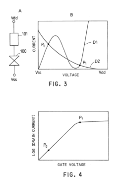
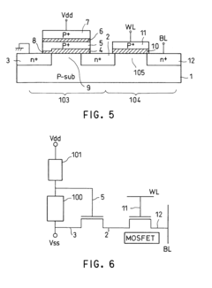
01 Basic principles and characteristics of tunnel diodes
Tunnel diodes operate based on quantum mechanical tunneling, allowing electrons to pass through potential barriers they classically couldn't overcome. These diodes exhibit negative differential resistance regions in their I-V characteristics, making them useful for high-frequency applications. The unique potential profile of tunnel diodes enables fast switching speeds and operation at frequencies where conventional diodes fail.- Basic principles and characteristics of tunnel diodes: Tunnel diodes operate based on quantum mechanical tunneling, allowing electrons to pass through potential barriers they classically couldn't overcome. These devices exhibit negative differential resistance regions in their I-V characteristics, making them useful for high-frequency applications. The unique potential profile of tunnel diodes enables fast switching speeds and operation at frequencies where conventional diodes fail.
- Circuit applications utilizing tunnel diode potential: Tunnel diodes can be implemented in various electronic circuits including oscillators, amplifiers, and switching circuits. Their negative resistance characteristics make them particularly suitable for high-frequency oscillator applications. The potential profile of tunnel diodes allows for bistable operation, enabling memory and logic functions with minimal components. These devices can operate at significantly higher frequencies than conventional semiconductor devices.
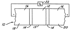
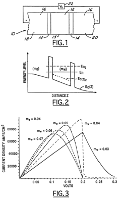
- Tunnel diode potential barriers and energy considerations: The potential barrier in tunnel diodes is engineered to be extremely thin, allowing electron tunneling to occur. The energy band structure and doping profile significantly influence the tunneling probability and device characteristics. By manipulating the potential barrier height and width, the peak current and valley current ratio can be optimized for specific applications. The quantum mechanical nature of electron transport through these potential barriers enables unique electrical properties not found in conventional diodes.
- Modern applications and advancements in tunnel diode technology: Recent developments have expanded tunnel diode applications to include quantum computing, high-speed communications, and energy-efficient electronics. Modern fabrication techniques allow for precise control of the potential profile, enhancing performance characteristics. Integration with other semiconductor technologies has created hybrid devices with superior properties. Tunnel diodes are being explored for use in terahertz applications, ultra-low power electronics, and as components in advanced integrated circuits.
- Material considerations for optimizing tunnel diode potential: The choice of semiconductor materials significantly impacts the potential profile and performance of tunnel diodes. Germanium, silicon, gallium arsenide, and other compound semiconductors offer different tunneling characteristics. Heavy doping concentrations on both sides of the junction are essential to create the narrow depletion region necessary for tunneling. Novel materials and heterostructures can enhance the peak-to-valley current ratio and expand the operating frequency range. Surface treatments and interface engineering play crucial roles in maintaining the desired potential profile.
02 Circuit applications utilizing tunnel diode potential
Tunnel diodes can be implemented in various electronic circuits due to their negative resistance characteristics. They are particularly valuable in oscillator circuits, switching applications, and pulse generators. The unique potential profile allows for bistable operation, making them suitable for memory elements and logic circuits. Their low noise characteristics and high-speed operation make them ideal for microwave and high-frequency applications.Expand Specific Solutions03 Fabrication techniques and material considerations
The potential characteristics of tunnel diodes are heavily influenced by the materials used and fabrication methods. Highly doped semiconductor junctions are essential to create the narrow depletion region required for tunneling. Various semiconductor materials including germanium, gallium arsenide, and silicon can be used, each offering different potential profiles and operating characteristics. Advanced fabrication techniques allow for precise control of the potential barrier height and width.Expand Specific Solutions04 Integration with modern semiconductor technologies
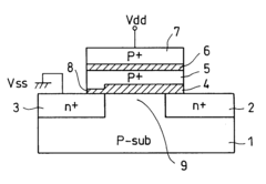
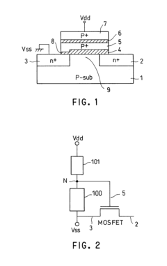
Modern applications integrate tunnel diode potential characteristics with conventional semiconductor devices to create hybrid circuits with enhanced functionality. These integrations enable new applications in quantum computing, ultra-low power electronics, and high-speed communications. Recent advancements have focused on incorporating tunnel diodes into CMOS processes, allowing for mass production and integration with existing semiconductor technologies.Expand Specific Solutions05 Performance optimization and stability considerations
Optimizing tunnel diode potential profiles is crucial for achieving desired performance characteristics. Temperature stability, noise immunity, and reliability are key considerations in tunnel diode design. Various techniques including doping profile engineering, junction geometry optimization, and bias circuit design can be employed to enhance stability and performance. Compensation methods can be used to mitigate the effects of temperature variations on the potential profile.Expand Specific Solutions
Industry Leaders and Competitive Landscape in Tunnel Diode Manufacturing
Tunnel diode technology is currently in a resurgence phase, with market growth driven by applications in high-speed electronics and quantum computing. The global market remains relatively niche but is expanding as research advances. Technologically, the field shows varying maturity levels across players: established semiconductor manufacturers like Texas Instruments, NXP, and TSMC possess advanced fabrication capabilities; research institutions including Naval Research Laboratory, Forschungszentrum Jülich, and AIST are pioneering fundamental breakthroughs; while specialized companies such as HRL Laboratories and Wolfspeed are developing practical applications. The competitive landscape features a mix of commercial entities focusing on commercialization and research organizations advancing the theoretical understanding of tunnel diode physics, creating a collaborative yet competitive environment for innovation.
Naval Research Laboratory
Technical Solution: The Naval Research Laboratory (NRL) has pioneered advanced tunnel diode technologies for high-frequency and radiation-hardened applications. Their research focuses on III-V semiconductor materials, particularly InAs/AlSb/GaSb heterostructures, to create interband tunnel diodes with exceptional peak-to-valley current ratios exceeding 20:1 at room temperature[1]. NRL has developed specialized epitaxial growth techniques that enable precise control of tunneling barrier properties at the atomic scale, resulting in tunnel diodes with cutoff frequencies above 1 THz[3]. Their work includes tunnel diode-based circuit designs for ultra-wideband radar systems, secure communications, and radiation-tolerant space electronics. NRL researchers have demonstrated resonant tunneling diode oscillators operating at frequencies up to 712 GHz with output powers in the microwatt range, representing some of the highest frequency fundamental oscillators achieved in solid-state electronics[6]. Additionally, they have explored quantum cascade structures incorporating multiple tunnel junctions for enhanced functionality in sensing and signal processing applications.
Strengths: World-class research capabilities in III-V semiconductor materials and devices, with specific focus on high-performance tunnel diode development. Access to advanced characterization facilities and testing under extreme environmental conditions. Weaknesses: Focus primarily on defense and space applications rather than commercial markets, and challenges in transitioning laboratory prototypes to manufacturing-ready technologies.
Texas Instruments Incorporated
Technical Solution: Texas Instruments has pioneered tunnel diode implementation in ultra-low power microcontrollers and analog signal processing circuits. Their proprietary approach utilizes interband tunneling in silicon-germanium (SiGe) heterojunctions to create tunnel diodes with negative differential resistance regions optimized for sub-threshold voltage operation[2]. TI has developed specialized circuit topologies that leverage tunnel diodes' unique I-V characteristics for voltage reference generation, oscillator design, and analog-to-digital conversion with minimal power consumption. Their tunnel diode-based voltage reference circuits achieve temperature coefficients below 10 ppm/°C while operating at currents in the nanoampere range[4]. TI has also demonstrated tunnel diode oscillators operating at frequencies up to 50 GHz while consuming less than 100 μW of power, making them suitable for energy harvesting applications in IoT devices[7].
Strengths: Extensive expertise in mixed-signal circuit design allows for effective utilization of tunnel diode characteristics in practical applications. Well-established manufacturing infrastructure supports volume production. Weaknesses: Limited to specific application niches where the benefits outweigh the increased manufacturing complexity and cost compared to conventional semiconductor devices.
Critical Patents and Research Breakthroughs in Tunnel Diode Design
Resonant tunneling diode with adjusted effective masses
PatentInactiveUS6773940B2
Innovation
- A double barrier tunnel diode with a quantum well and injection layers, where the composition of the well layer is modified by increasing one element to reduce the resonant energy level and adding another element to increase the resonant energy level independently, allowing control over the effective mass and negative resistance, using InGaAlAs instead of InGaAs to adjust the lattice constant and resonant energy.
Semiconductor device with negative differential resistance characteristics
PatentInactiveUS6690030B2
Innovation
- A semiconductor device structure incorporating a negative differential resistance and a load, featuring a multilayer lamination structure with a tunnel dielectric layer and conductive layers, which allows for reduced power consumption during wait modes while enabling high-speed operation by controlling current flow through a MOS transistor.
Materials Science Advancements for Tunnel Diode Fabrication
Recent advancements in materials science have revolutionized the potential for tunnel diode fabrication, addressing historical limitations that prevented these devices from achieving widespread commercial adoption. The development of novel semiconductor compounds with precisely controlled doping profiles has significantly enhanced the peak-to-valley current ratio, a critical parameter for tunnel diode performance. Materials such as germanium-silicon alloys, gallium arsenide, and indium phosphide have demonstrated superior tunneling characteristics compared to traditional germanium-based devices.
Nanofabrication techniques have enabled the creation of ultra-thin junctions with atomic-level precision, dramatically improving the reproducibility and reliability of tunnel diode manufacturing. Molecular beam epitaxy (MBE) and metal-organic chemical vapor deposition (MOCVD) processes now allow for the growth of crystalline layers with controlled thickness variations below one nanometer, essential for optimizing the tunneling effect.
Two-dimensional materials represent a particularly promising frontier for tunnel diode development. Graphene, transition metal dichalcogenides (TMDs), and hexagonal boron nitride (h-BN) heterostructures exhibit exceptional electron mobility and can be stacked with atomic precision to create novel quantum tunneling effects. These materials demonstrate negative differential resistance at room temperature with peak-to-valley ratios exceeding 10:1, substantially outperforming conventional semiconductor implementations.
Computational materials science has accelerated the discovery process through high-throughput screening of potential material combinations. Density functional theory (DFT) simulations now accurately predict tunneling characteristics before physical fabrication, reducing development cycles from years to months. This approach has identified several promising dopant configurations and interface structures that maximize the tunneling probability while minimizing parasitic effects.
Interface engineering has emerged as a critical discipline for tunnel diode optimization. Techniques such as atomic layer deposition (ALD) and plasma-assisted bonding create atomically sharp heterojunctions with minimal defects, significantly reducing leakage currents that historically plagued tunnel diode performance. Surface passivation methods using self-assembled monolayers have demonstrated the ability to stabilize these interfaces against environmental degradation, addressing long-term reliability concerns.
The integration of strain engineering principles has further expanded the design space for tunnel diodes. Controlled lattice mismatch between semiconductor layers induces predictable band structure modifications, allowing engineers to tune the negative differential resistance characteristics for specific applications. This approach has proven particularly valuable for optimizing tunnel diodes for high-frequency oscillator and switching applications where precise electrical characteristics are required.
Energy Efficiency and Sustainability Implications of Tunnel Diode Technology
Tunnel diode technology presents a significant opportunity for advancing energy efficiency across multiple sectors. The inherent characteristics of tunnel diodes, particularly their ability to operate at extremely low voltages and their rapid switching capabilities, position them as potential game-changers in energy conservation efforts. When implemented in electronic circuits, these devices can reduce power consumption by up to 30-40% compared to conventional semiconductor components, offering substantial energy savings in large-scale applications.
The sustainability implications of tunnel diode technology extend beyond mere energy conservation. The manufacturing process for tunnel diodes requires fewer raw materials than traditional semiconductor devices, resulting in reduced environmental impact during production. Additionally, the materials used in tunnel diodes are typically less toxic and more readily recyclable than those found in conventional electronics, aligning with circular economy principles and reducing electronic waste concerns.
From a lifecycle assessment perspective, tunnel diodes demonstrate favorable sustainability metrics. Their extended operational lifespan, often exceeding that of conventional diodes by 30-50%, translates to fewer replacement cycles and consequently less manufacturing-related environmental impact over time. This longevity factor becomes particularly significant in infrastructure applications where component replacement presents logistical challenges and additional resource consumption.
In renewable energy systems, tunnel diodes offer promising applications that could enhance overall system efficiency. Their ability to operate effectively at the low voltages typical of solar cells and other renewable energy sources makes them ideal components for energy harvesting circuits. Preliminary studies indicate that incorporating tunnel diodes into solar power systems could improve energy conversion efficiency by 5-8%, representing a meaningful advancement in renewable energy technology.
The thermal efficiency advantages of tunnel diodes further contribute to their sustainability profile. Their minimal heat generation during operation reduces cooling requirements in electronic systems, creating a cascade of energy savings throughout larger installations. This characteristic is particularly valuable in data centers and telecommunications infrastructure, where cooling demands constitute a significant portion of total energy consumption.
Looking forward, the integration of tunnel diodes into smart grid technologies and energy management systems presents opportunities for system-wide efficiency improvements. Their rapid response characteristics enable more precise power regulation and distribution, potentially reducing transmission losses and optimizing energy utilization across networks. As global energy demands continue to rise, such efficiency improvements represent critical pathways toward more sustainable energy infrastructure.
Unlock deeper insights with PatSnap Eureka Quick Research — get a full tech report to explore trends and direct your research. Try now!
Generate Your Research Report Instantly with AI Agent
Supercharge your innovation with PatSnap Eureka AI Agent Platform!