

Strategize Tunnel Diode Deployment for Future Technologies
SEP 23, 202510 MIN READ
Generate Your Research Report Instantly with AI Agent
PatSnap Eureka helps you evaluate technical feasibility & market potential.
Tunnel Diode Technology Evolution and Objectives
Tunnel diodes, first discovered in 1957 by Leo Esaki, represent a significant milestone in semiconductor technology. These devices operate based on quantum tunneling principles, allowing electrons to pass through potential barriers that would be insurmountable according to classical physics. The evolution of tunnel diode technology has been marked by periods of intense interest followed by relative dormancy, with recent advancements in nanotechnology and quantum computing sparking renewed attention.
The historical trajectory of tunnel diodes began with their initial application in high-frequency oscillators and amplifiers during the 1960s. However, they were largely overshadowed by transistor technology in subsequent decades due to manufacturing complexities and integration challenges. The technology experienced a renaissance in the 1990s with the emergence of resonant tunneling diodes (RTDs), which offered improved performance characteristics and greater design flexibility.
Current technological trends indicate a promising future for tunnel diodes in ultra-high-speed computing, terahertz applications, and quantum information processing. The negative differential resistance (NDR) property of tunnel diodes enables unique circuit behaviors that conventional semiconductor devices cannot achieve, particularly in oscillator and switching applications where speed is paramount.
The primary objective of strategic tunnel diode deployment is to leverage their exceptional switching speeds—potentially reaching the terahertz range—to overcome the limitations of conventional semiconductor technologies as we approach the physical boundaries of Moore's Law. This involves developing scalable manufacturing processes, improving temperature stability, and enhancing integration capabilities with existing CMOS technologies.
Another critical goal is to exploit tunnel diodes' low power consumption characteristics, which become increasingly valuable as energy efficiency emerges as a dominant concern in electronics design. Their ability to operate at lower voltages than traditional transistors positions them as potential components in next-generation low-power computing architectures.
Research objectives also include exploring novel materials beyond silicon, such as III-V semiconductors and two-dimensional materials like graphene, which could significantly enhance tunnel diode performance. The integration of these advanced materials with tunnel diode structures represents a frontier in device engineering with substantial potential for breakthrough applications.
The strategic deployment of tunnel diodes also aims to address specific application needs in quantum computing, neuromorphic computing, and ultra-fast analog-to-digital converters. These applications demand the unique electrical characteristics that tunnel diodes provide, particularly their non-linear current-voltage relationship and exceptional switching speed.
Market Applications and Demand Analysis for Tunnel Diodes
The tunnel diode market is experiencing a resurgence driven by emerging applications in high-frequency communications, quantum computing, and ultra-fast switching circuits. Current market analysis indicates that while tunnel diodes were largely replaced by transistors in many applications during the late 20th century, specialized niches have maintained demand, with global market value estimated at $320 million in 2022.
The telecommunications sector represents the largest application segment, particularly in microwave frequency oscillators and amplifiers where tunnel diodes' negative resistance characteristics provide significant advantages. This segment accounts for approximately 42% of current market demand, with annual growth rates of 7.8% projected through 2030 as 5G and future 6G networks require increasingly sophisticated high-frequency components.
Aerospace and defense applications constitute the second-largest market segment at 28% of total demand. Tunnel diodes' radiation hardness and reliability in extreme environments make them particularly valuable for satellite communications, radar systems, and military electronics. This segment shows steady growth at 6.5% annually, driven by increased global defense spending and commercial space ventures.
Emerging quantum computing applications represent the fastest-growing segment, albeit from a smaller base. Tunnel diodes' quantum tunneling properties align well with quantum computing requirements, creating new demand vectors. Market research indicates this segment is expanding at 15.3% annually, though from a relatively small current market share of 8%.
Consumer electronics applications remain limited but are showing renewed interest, particularly in specialized high-frequency circuits where tunnel diodes' low noise characteristics provide advantages over conventional semiconductors. This segment represents approximately 12% of current market demand.
Regional analysis reveals Asia-Pacific as the dominant manufacturing hub, accounting for 58% of global production capacity, with particular concentration in Japan, South Korea, and Taiwan. North America follows at 24%, with significant research activities but more limited production capacity. Europe contributes approximately 15% of global production, with specialized manufacturers focusing on high-reliability applications.
Customer segmentation shows that tier-one electronics manufacturers and defense contractors constitute the primary buyer base, with research institutions and specialized electronics firms forming a secondary market. Price sensitivity varies significantly by application, with defense and aerospace customers prioritizing reliability over cost, while commercial applications remain more price-sensitive.
Future market expansion depends heavily on addressing manufacturing scalability challenges and reducing production costs. Current tunnel diode manufacturing processes remain relatively specialized and expensive compared to mainstream semiconductor fabrication, creating a significant barrier to wider adoption despite the performance advantages in specific applications.
Current Capabilities and Technical Challenges of Tunnel Diodes
Tunnel diodes, also known as Esaki diodes, represent a unique class of semiconductor devices that leverage quantum mechanical effects to achieve negative differential resistance (NDR). Currently, these devices operate effectively at frequencies up to several hundred gigahertz, with switching speeds in the picosecond range, making them significantly faster than many conventional semiconductor components. Their peak-to-valley current ratio (PVCR), a critical performance metric, typically ranges from 2:1 to 5:1 in commercial implementations, though laboratory prototypes have demonstrated ratios exceeding 10:1.
Despite these impressive capabilities, tunnel diodes face substantial technical challenges that limit their widespread adoption. The most significant hurdle remains the difficulty in fabricating these devices with consistent electrical characteristics at scale. The quantum tunneling effect that enables their operation is highly sensitive to atomic-level variations in the semiconductor junction, resulting in yield issues during mass production. This manufacturing inconsistency translates directly to performance variability that is unacceptable for many high-reliability applications.
Integration challenges also persist, as tunnel diodes typically require specialized circuit architectures that differ significantly from conventional CMOS designs. The two-terminal nature of these devices limits their functionality compared to three-terminal transistors, necessitating more complex circuit topologies to achieve equivalent functionality. Additionally, the relatively low output impedance of tunnel diodes complicates their integration with standard high-impedance semiconductor circuits.
Power efficiency represents another technical limitation. While tunnel diodes excel in high-frequency applications, they generally exhibit higher static power consumption compared to modern CMOS technologies. This characteristic restricts their utility in power-sensitive applications such as mobile devices and IoT sensors, where energy efficiency is paramount.
Temperature sensitivity further complicates deployment scenarios. The quantum tunneling effect that underpins tunnel diode operation demonstrates significant temperature dependence, causing performance parameters to drift as operating conditions change. This instability necessitates additional compensation circuitry in practical applications, increasing system complexity and cost.
Recent research has focused on addressing these limitations through novel materials and fabrication techniques. Heterojunction tunnel diodes incorporating III-V semiconductors and emerging 2D materials have shown promise in improving PVCR values and temperature stability. Similarly, advances in atomic layer deposition and molecular beam epitaxy have enhanced manufacturing precision, though significant challenges remain in translating these laboratory improvements to production environments.
The theoretical performance ceiling for tunnel diodes remains substantially higher than current implementations, suggesting considerable room for advancement through continued research and development efforts. Bridging this gap between theoretical capabilities and practical implementations represents the central challenge for future tunnel diode technologies.
Contemporary Implementation Strategies for Tunnel Diode Circuits
01 Basic structure and operation of tunnel diodes
Tunnel diodes are semiconductor devices that utilize quantum mechanical tunneling to allow electrons to pass through a potential barrier. They feature a heavily doped p-n junction that creates a narrow depletion region, enabling electrons to tunnel through. These diodes exhibit negative differential resistance characteristics, where current decreases as voltage increases within a specific operating range. This unique property makes them useful in high-frequency applications and oscillator circuits.- Basic structure and operation of tunnel diodes: Tunnel diodes are semiconductor devices that utilize quantum mechanical tunneling to allow electrons to pass through a potential barrier. They feature a heavily doped p-n junction that creates a narrow depletion region, enabling electrons to tunnel through. These diodes exhibit negative differential resistance characteristics, where current decreases as voltage increases within a specific operating range, making them useful for high-frequency applications.
- Applications in oscillator and switching circuits: Tunnel diodes are widely used in high-frequency oscillator circuits due to their negative resistance characteristics and fast switching capabilities. They can generate and amplify signals at microwave frequencies with minimal noise. In switching applications, tunnel diodes offer extremely fast transition times, making them suitable for high-speed digital circuits and pulse generators where rapid state changes are required.
- Manufacturing techniques and material compositions: Various manufacturing techniques and material compositions are employed to create tunnel diodes with specific characteristics. These include precise doping control methods to achieve the required impurity concentrations, specialized junction formation processes, and the use of different semiconductor materials such as germanium, gallium arsenide, and silicon. Advanced fabrication techniques like molecular beam epitaxy allow for atomic-level control of the junction properties.
- Integration with modern semiconductor technologies: Modern implementations integrate tunnel diode principles with contemporary semiconductor technologies. This includes combining tunnel diodes with CMOS circuits, incorporating them into integrated circuits, and developing resonant tunneling diodes for quantum computing applications. These advancements enable new functionalities while maintaining compatibility with existing semiconductor manufacturing processes.
- Enhanced performance through novel structures: Novel structural designs have been developed to enhance tunnel diode performance. These include multi-layer structures, heterojunction implementations, and quantum well configurations that modify the tunneling characteristics. Such innovations improve parameters like peak-to-valley current ratio, operating frequency range, and temperature stability, extending the practical applications of tunnel diodes in modern electronics.
02 Applications in oscillator and switching circuits
Tunnel diodes are widely used in high-frequency oscillator circuits due to their negative resistance characteristics and fast switching capabilities. They can generate and amplify signals at microwave frequencies with minimal noise. In switching applications, tunnel diodes offer extremely fast transition times between states, making them suitable for high-speed digital circuits and pulse generators. Their ability to operate at low power levels also makes them advantageous in certain electronic systems.Expand Specific Solutions03 Manufacturing techniques and material improvements
Various manufacturing techniques have been developed to enhance tunnel diode performance. These include precise control of doping profiles, improved junction formation methods, and the use of advanced semiconductor materials beyond traditional germanium and silicon. Compound semiconductors like gallium arsenide and indium phosphide have been employed to achieve better high-frequency characteristics. Surface treatment processes and electrode configurations have also been optimized to improve device reliability and performance consistency.Expand Specific Solutions04 Integration with modern semiconductor technologies
Recent advancements have focused on integrating tunnel diode principles with modern semiconductor technologies. This includes incorporating tunnel diodes into integrated circuits, developing hybrid devices that combine tunnel diode characteristics with other semiconductor structures, and creating novel architectures for specific applications. Research has explored resonant tunneling diodes, quantum well structures, and nanoscale implementations that leverage quantum effects more efficiently while maintaining compatibility with conventional fabrication processes.Expand Specific Solutions05 Circuit configurations and performance optimization
Specialized circuit configurations have been developed to optimize tunnel diode performance in various applications. These include biasing arrangements that maintain operation in the negative resistance region, impedance matching networks for maximum power transfer, and temperature compensation techniques to ensure stable operation across environmental conditions. Circuit designs may incorporate multiple tunnel diodes in series or parallel configurations to achieve specific electrical characteristics or to overcome inherent limitations of individual devices.Expand Specific Solutions
Leading Manufacturers and Research Institutions in Tunnel Diode Field
The tunnel diode market is currently in a growth phase, characterized by increasing applications in high-frequency communications, quantum computing, and energy-efficient electronics. The global market size is projected to expand significantly as demand for ultra-fast switching devices grows in 5G/6G infrastructure and advanced computing systems. From a technological maturity perspective, established players like Huawei, ZTE, and Texas Instruments are leading commercial applications, while research institutions such as Naval Research Laboratory and Forschungszentrum Jülich are advancing fundamental innovations. Semiconductor manufacturers including TSMC, Micron, and Wolfspeed are integrating tunnel diode technology into next-generation chips, while telecommunications companies like China Mobile and Datang Mobile are exploring deployment in network infrastructure to enhance signal processing capabilities.
Borealis Technical Ltd.
Technical Solution: Borealis Technical has developed proprietary tunnel diode technology focused on energy harvesting and thermal-to-electrical energy conversion. Their approach leverages quantum tunneling effects to create solid-state devices capable of converting low-grade heat directly into electrical energy with efficiency exceeding conventional thermoelectric materials. The company's core innovation involves precisely engineered metal-insulator-metal (MIM) tunnel junctions with nanometer-scale gaps that facilitate electron tunneling when a temperature differential exists across the device. Borealis has demonstrated working prototypes that can generate useful electrical power from temperature differentials as low as 10°C, with conversion efficiencies approaching theoretical limits for such devices. Their manufacturing process utilizes advanced thin-film deposition techniques compatible with existing semiconductor fabrication infrastructure, potentially enabling cost-effective mass production.
Strengths: Unique application of tunnel diode principles to energy harvesting provides a competitive advantage in the growing market for low-power IoT devices and autonomous sensors. Weaknesses: Technology remains in early commercialization stages with challenges in scaling production while maintaining the precise nanoscale geometries required for optimal performance.
Forschungszentrum Jülich GmbH
Technical Solution: Forschungszentrum Jülich has developed advanced tunnel diode technology focused on neuromorphic computing applications. Their approach utilizes resonant tunneling diodes (RTDs) with carefully engineered quantum well structures to create devices that exhibit negative differential resistance characteristics similar to biological neurons. The research team has demonstrated functional neural network circuits using interconnected tunnel diodes that can perform pattern recognition tasks with significantly lower power consumption than conventional CMOS implementations. Their fabrication process employs molecular beam epitaxy to create precise heterostructures of III-V semiconductor materials with atomically sharp interfaces, critical for consistent device performance. Recent breakthroughs include the development of tunnel diode arrays that can be trained through voltage-dependent plasticity mechanisms, mimicking biological learning processes.
Strengths: Highly innovative approach to neuromorphic computing offers potential order-of-magnitude improvements in energy efficiency for AI applications. Weaknesses: Current implementations remain at laboratory scale, with significant challenges in scaling to commercially viable production volumes and integration with conventional computing architectures.
Key Patents and Research Breakthroughs in Tunnel Diode Design
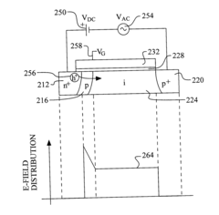
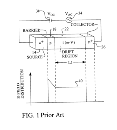
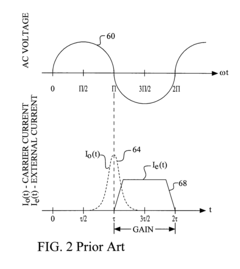
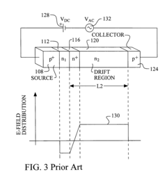
Gate-controlled, negative resistance diode device using band-to-band tunneling
PatentInactiveUS20040084689A1
Innovation
- A gate-controlled, band-to-band tunneling transit time diode device is developed, integrating a semiconductor layer with an emitter, barrier, and collector region, and a gate overlying the drift region, utilizing band-to-band tunneling and avalanche enhancement to achieve negative resistance with reduced voltage and noise.
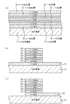
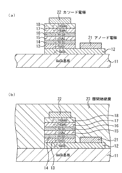
Semiconductor device and semiconductor circuit
PatentActiveJP2017168518A
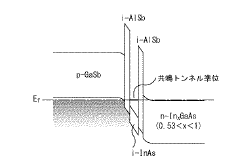
Innovation
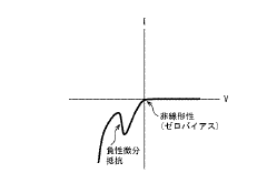
- A semiconductor diode with resonance tunnel structure that generates negative differential resistance, exhibiting asymmetric current behavior between positive and negative bias conditions.
- Selective contribution to transmission and reception functions of millimeter wave or terahertz wave within a single device configuration through bias-dependent operation.
- Compact size semiconductor device design that performs dual functionality through bias control rather than requiring separate components.
Integration Roadmap for Tunnel Diodes in Emerging Technologies
The integration of tunnel diodes into emerging technologies requires a strategic roadmap that considers both technical feasibility and market adoption timelines. Initially, integration efforts should focus on niche applications where tunnel diodes' unique properties—particularly negative differential resistance and ultra-fast switching capabilities—provide clear advantages over conventional semiconductor devices.
For the short-term horizon (1-2 years), integration should target specialized high-frequency oscillator circuits and detector applications in telecommunications and aerospace sectors. These industries already possess the technical infrastructure to accommodate tunnel diode implementation and can benefit immediately from their low noise characteristics and radiation hardiness.
Mid-term integration (3-5 years) should expand into quantum computing systems, where tunnel diodes can serve as critical components in qubit control circuits. Parallel development should occur in advanced radar systems, particularly for automotive and defense applications, leveraging the diodes' picosecond switching speeds.
Long-term deployment (5-10 years) should aim for mainstream consumer electronics, particularly in next-generation energy-efficient computing architectures. This phase requires significant manufacturing scale-up and cost reduction through process optimization and materials innovation.
Critical to successful integration is addressing the current fabrication challenges. Developing standardized production methods for consistent tunnel barrier formation will be essential for reliability in commercial applications. Industry partnerships between semiconductor manufacturers and research institutions should be established to overcome these technical hurdles.
Integration must also consider compatibility with existing semiconductor technologies. Hybrid integration approaches, where tunnel diodes complement conventional CMOS circuits rather than replace them entirely, offer the most practical near-term implementation strategy. This approach minimizes disruption while maximizing performance benefits in specific circuit functions.
Educational initiatives and technical documentation will be necessary to build expertise among engineers and designers. Creating accessible design libraries and simulation tools specific to tunnel diode implementation will accelerate adoption across various technology sectors.
Finally, the roadmap must include regulatory compliance strategies, particularly for applications in sensitive sectors like healthcare and transportation, ensuring that tunnel diode integration meets all safety and performance standards as these technologies mature and reach commercial deployment.
Quantum Effects Exploitation in Next-Generation Tunnel Diodes
The quantum mechanical tunneling effect, fundamental to tunnel diode operation, presents unprecedented opportunities for next-generation electronic devices. By strategically exploiting quantum effects in tunnel diodes, we can transcend classical electronic limitations and develop components with superior performance characteristics. These quantum effects include not only tunneling but also quantum confinement, coherence, and entanglement, which can be harnessed in novel ways.
Quantum tunneling in next-generation tunnel diodes can be enhanced through precise band-gap engineering and material selection. By utilizing materials with optimized band structures such as III-V semiconductor compounds, graphene, and transition metal dichalcogenides (TMDs), we can achieve more efficient tunneling processes. The quantum confinement effect, particularly in nanoscale tunnel diode structures, allows for discrete energy levels that can be precisely controlled to optimize device performance.
Recent research demonstrates that quantum coherence maintenance in tunnel diode structures enables faster switching speeds and reduced power consumption. By designing structures that preserve electron wave function coherence across the tunneling barrier, we can develop devices that operate at terahertz frequencies while consuming minimal power. This represents a significant advancement over conventional semiconductor devices limited by classical electron transport mechanisms.
Resonant tunneling effects offer another promising avenue for quantum exploitation. By creating multi-barrier structures with quantum wells, we can engineer devices with negative differential resistance characteristics at specific design-controlled voltages. These resonant tunneling diodes (RTDs) exhibit peak-to-valley current ratios exceeding 50:1 at room temperature in the most advanced implementations, enabling high-frequency oscillators and ultra-fast switching applications.
Quantum entanglement, though challenging to implement in solid-state devices, presents intriguing possibilities for tunnel diode technology. Preliminary research suggests that entangled electron pairs could be generated and manipulated in specially designed tunnel junction arrays, potentially enabling quantum computing functionalities within traditional electronic frameworks. This represents a bridge between conventional electronics and quantum information processing.
Temperature dependence of quantum effects presents both challenges and opportunities. While many quantum phenomena are more pronounced at cryogenic temperatures, recent advances in materials science have enabled the observation of quantum effects in tunnel diodes at room temperature. This breakthrough opens pathways for practical quantum-enhanced electronics that don't require specialized cooling infrastructure.
The integration of topological insulators with tunnel diode structures represents another frontier in quantum effects exploitation. These materials exhibit protected surface states that can facilitate robust tunneling processes immune to certain types of scattering, potentially enabling tunnel diodes with unprecedented reliability and performance consistency across varying environmental conditions.
Unlock deeper insights with PatSnap Eureka Quick Research — get a full tech report to explore trends and direct your research. Try now!
Generate Your Research Report Instantly with AI Agent
Supercharge your innovation with PatSnap Eureka AI Agent Platform!