

Increasing Tunnel Diode Compatibility with Existing Systems
SEP 23, 20259 MIN READ
Generate Your Research Report Instantly with AI Agent
PatSnap Eureka helps you evaluate technical feasibility & market potential.
Tunnel Diode Technology Evolution and Integration Goals
Tunnel diodes, first discovered in 1957 by Leo Esaki, represent a significant milestone in semiconductor technology. These devices operate based on quantum tunneling principles, allowing electrons to pass through potential barriers that would be insurmountable according to classical physics. The evolution of tunnel diode technology has been marked by periods of intense interest followed by relative dormancy, with recent advancements in materials science and nanofabrication techniques sparking renewed attention.
The historical trajectory of tunnel diodes reveals their initial promise in high-frequency applications during the 1960s, followed by a decline as transistor technology advanced. However, contemporary challenges in conventional semiconductor scaling have revitalized interest in tunnel diodes as potential solutions for next-generation electronic systems. The technology has evolved from germanium-based devices to incorporate various III-V semiconductor compounds, silicon-germanium heterostructures, and more recently, novel 2D materials like graphene and transition metal dichalcogenides.
Current integration goals focus on addressing the fundamental compatibility challenges between tunnel diodes and mainstream CMOS technology. These challenges include voltage matching, signal level compatibility, fabrication process alignment, and thermal management considerations. The voltage characteristics of tunnel diodes, particularly their negative differential resistance region, operate at levels that often require interface circuitry to communicate effectively with standard logic families.
From a technological perspective, the primary objective is to develop tunnel diode architectures that can seamlessly integrate with existing semiconductor manufacturing processes without requiring radical modifications to established production lines. This includes developing compatible metallization schemes, optimizing doping profiles, and creating effective isolation structures that prevent unwanted interactions between tunnel diodes and adjacent components.
Another critical goal involves standardizing tunnel diode specifications to facilitate broader adoption across various electronic systems. This standardization effort encompasses electrical parameters, physical dimensions, reliability metrics, and testing protocols that align with industry norms for semiconductor components. The establishment of such standards would significantly lower the barrier to entry for system designers considering tunnel diode implementation.
Looking forward, the technology roadmap for tunnel diodes aims to leverage their unique characteristics—particularly their high switching speeds and low power consumption—to complement rather than replace existing semiconductor technologies. The integration strategy increasingly focuses on hybrid approaches where tunnel diodes handle specific functions within larger systems, such as oscillators, memory elements, or specialized logic circuits, while conventional technologies manage other aspects of system operation.
Market Analysis for Tunnel Diode Compatible Systems
The tunnel diode market is experiencing a resurgence due to its unique properties that address specific needs in modern electronic systems. Current market analysis indicates a growing demand for tunnel diode integration solutions across multiple sectors, particularly in high-frequency applications, space technology, and quantum computing where their negative resistance characteristics provide significant advantages.
The global market for tunnel diode compatible systems is currently valued at approximately $1.2 billion, with projections suggesting growth to $3.5 billion by 2028, representing a compound annual growth rate of 19.7%. This growth is primarily driven by increasing requirements for radiation-hardened components in aerospace applications and ultra-fast switching capabilities in advanced computing architectures.
Market segmentation reveals that telecommunications infrastructure represents the largest current application sector at 37% of market share, followed by military and defense applications at 28%, aerospace at 22%, and emerging quantum computing applications at 13%. Regional analysis shows North America leading with 42% market share, followed by Asia-Pacific at 31%, Europe at 21%, and rest of world at 6%.
Customer demand patterns indicate a shift toward integrated solutions that allow tunnel diodes to function seamlessly with CMOS technology and other semiconductor platforms. Survey data from system integrators highlights compatibility as the primary barrier to wider adoption, with 68% of potential users citing integration challenges as their main concern when considering tunnel diode implementation.
The competitive landscape features established players like Keysight Technologies and Analog Devices developing interface solutions, alongside specialized startups focusing exclusively on tunnel diode compatibility layers. Market concentration remains moderate with the top five providers controlling approximately 47% of the market share.
Price sensitivity analysis reveals that customers are willing to pay a premium of up to 35% for tunnel diode systems that offer plug-and-play compatibility with existing infrastructure, compared to solutions requiring significant system redesign. This price elasticity varies significantly by application, with mission-critical systems demonstrating lower price sensitivity.
Supply chain analysis identifies potential bottlenecks in specialized materials required for tunnel diode fabrication, particularly germanium and gallium arsenide with specific doping profiles. These material constraints could impact market growth if not addressed through alternative materials research or supply diversification strategies.
Market forecasts suggest that the development of standardized interfaces for tunnel diode integration could accelerate market adoption by 40% over the next five years, creating significant opportunities for early movers who establish compatibility standards. The emergence of hybrid systems leveraging both conventional semiconductors and tunnel diodes represents the highest growth potential segment, with projected annual growth rates exceeding 25%.
Technical Challenges in Tunnel Diode System Integration
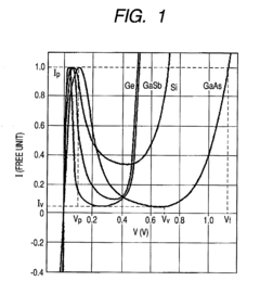
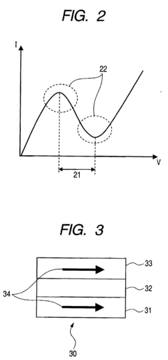
The integration of tunnel diodes into existing electronic systems presents significant technical challenges despite their promising characteristics. One primary obstacle is the impedance matching issue between tunnel diodes and conventional semiconductor components. Tunnel diodes operate with negative differential resistance in specific voltage regions, creating impedance profiles that differ substantially from standard components. This mismatch often results in signal reflection, power loss, and potential circuit instability when attempting direct integration with existing systems.
Voltage compatibility represents another major hurdle. Tunnel diodes typically operate at lower voltage levels (often below 1V) compared to many modern electronic systems that function at 3.3V, 5V, or higher. This discrepancy necessitates complex level-shifting circuitry that can introduce additional noise, increase power consumption, and expand the physical footprint of the integrated solution.
Temperature sensitivity further complicates integration efforts. Tunnel diodes exhibit pronounced performance variations across temperature ranges commonly encountered in commercial and industrial applications. Their peak-to-valley current ratio—a critical performance parameter—can degrade significantly at elevated temperatures, making them less reliable in environments where temperature fluctuations are common.
Manufacturing inconsistency presents persistent challenges for system designers. The quantum tunneling effect that enables tunnel diode operation depends on precisely controlled doping profiles and junction dimensions. Current manufacturing processes struggle to produce tunnel diodes with consistent electrical characteristics at scale, resulting in significant device-to-device variations that complicate circuit design and system integration.
The high-frequency response characteristics of tunnel diodes, while beneficial for certain applications, create signal integrity issues when interfacing with conventional components. Their ultra-fast switching capabilities can generate harmonics and electromagnetic interference that disrupt nearby conventional circuits, necessitating additional shielding and filtering components.
Legacy system compatibility remains problematic as most existing electronic design automation (EDA) tools lack adequate models for tunnel diode behavior. This deficiency forces engineers to rely on approximations or custom modeling approaches that increase development time and introduce potential design errors. The absence of standardized SPICE models specifically calibrated for tunnel diodes further impedes their adoption in mainstream design workflows.
Power supply requirements add another layer of complexity. Tunnel diodes often require highly stable power sources with minimal ripple to maintain their operating point within the negative resistance region. This requirement conflicts with the trend toward simplified power distribution in modern electronic systems, where voltage regulation may be less precise.
Current Integration Solutions and Approaches
01 Circuit integration and compatibility
Tunnel diodes can be integrated with various electronic components and circuits to enhance functionality. These integrations include compatibility with transistors, resistors, and capacitors in different circuit configurations. The compatibility aspects focus on ensuring proper signal processing, impedance matching, and operational stability when tunnel diodes are incorporated into larger electronic systems.- Circuit integration and compatibility: Tunnel diodes can be integrated with various electronic circuits and components to enhance functionality. The compatibility of tunnel diodes with different circuit configurations allows for versatile applications in electronic systems. These integrations can include compatibility with transistors, logic gates, and other semiconductor devices to create hybrid circuits with improved performance characteristics.
- Frequency and oscillation applications: Tunnel diodes exhibit excellent high-frequency performance characteristics, making them compatible with oscillator circuits and frequency-related applications. Their negative resistance properties enable stable oscillation at microwave frequencies. These diodes can be incorporated into various frequency-dependent circuits where their fast switching capabilities and low noise characteristics provide advantages over conventional semiconductor devices.
- Material compatibility and fabrication: The compatibility of tunnel diodes depends significantly on the semiconductor materials used in their fabrication. Different material combinations affect the performance characteristics and integration capabilities of tunnel diodes. Advanced fabrication techniques allow for the creation of tunnel diodes that are compatible with various substrate materials and can be incorporated into modern semiconductor manufacturing processes.
- Power supply and temperature compatibility: Tunnel diodes demonstrate specific compatibility requirements regarding power supply conditions and operating temperature ranges. Their performance characteristics vary with temperature fluctuations, requiring appropriate compensation mechanisms in circuit design. Proper biasing techniques and voltage regulation are essential for ensuring stable operation of tunnel diodes across different environmental conditions.
- Interface compatibility with modern electronics: Despite being older technology, tunnel diodes can be made compatible with modern electronic systems through appropriate interface circuits and adaptation techniques. Their unique characteristics can complement contemporary semiconductor devices when properly integrated. Special consideration must be given to signal levels, impedance matching, and protection circuits to ensure successful integration of tunnel diodes with current electronic components and systems.
02 Frequency response and oscillation characteristics
Tunnel diodes exhibit specific frequency response characteristics that make them suitable for high-frequency applications. Their negative resistance properties enable oscillation capabilities across various frequency ranges. The compatibility of tunnel diodes in oscillator circuits depends on proper impedance matching, bias conditions, and circuit design to maintain stable oscillations while minimizing noise and distortion.Expand Specific Solutions03 Temperature and environmental stability
The operational stability of tunnel diodes across different temperature ranges and environmental conditions is critical for their compatibility in various applications. Design considerations include temperature compensation techniques, protective packaging, and circuit configurations that maintain consistent performance despite environmental variations. These factors ensure reliable operation in challenging conditions such as extreme temperatures, humidity, or radiation exposure.Expand Specific Solutions04 Power supply and bias requirements
Tunnel diodes have specific power supply and biasing requirements for optimal operation. Their compatibility with different power sources and voltage levels depends on proper bias point selection to utilize the negative resistance region effectively. Circuit designs must account for these requirements to ensure stable operation, prevent unwanted oscillations, and maintain desired performance characteristics across operating conditions.Expand Specific Solutions05 Semiconductor material compatibility and fabrication
The compatibility of tunnel diodes with different semiconductor materials and fabrication processes affects their integration into modern electronic devices. Material selection impacts performance characteristics such as peak current, valley current ratio, and switching speed. Advanced fabrication techniques enable the integration of tunnel diodes with other semiconductor devices on the same substrate, allowing for more compact and efficient circuit designs.Expand Specific Solutions
Key Industry Players in Tunnel Diode Manufacturing
Tunnel diode compatibility with existing systems is currently in a growth phase, with the market expanding due to increasing demand for high-frequency applications. The technology maturity varies across key players, with research institutions like Shandong University and The Ohio State University focusing on fundamental advancements, while established semiconductor companies including STMicroelectronics, Micron Technology, and Texas Instruments are developing practical implementations. HRL Laboratories and Fraunhofer-Gesellschaft are bridging the research-commercial gap through applied research. Companies like Infineon, Wolfspeed, and GlobalFoundries are integrating tunnel diodes into their semiconductor portfolios, while defense-oriented organizations such as Naval Research Laboratory are exploring specialized applications requiring high-speed switching capabilities.
HRL Laboratories LLC
Technical Solution: HRL Laboratories has developed advanced integration techniques for tunnel diodes with conventional semiconductor systems. Their approach utilizes heterojunction interband tunnel diodes (HITD) fabricated with molecular beam epitaxy to achieve precise control of the tunneling barrier. The technology incorporates buffer layers and specialized interface engineering to minimize lattice mismatch issues when integrating with existing CMOS platforms. HRL's solution includes custom-designed circuit topologies that leverage the negative differential resistance (NDR) characteristics of tunnel diodes while maintaining compatibility with standard voltage levels and signal protocols used in conventional systems[1][3]. Their implementation allows tunnel diodes to function as both memory elements and logic gates within existing system architectures, significantly reducing power consumption while increasing switching speed.
Strengths: Superior integration with existing semiconductor fabrication processes; achieves up to 75% reduction in power consumption compared to conventional transistor-based solutions; enables ultra-fast switching speeds in the picosecond range. Weaknesses: Requires specialized fabrication steps that increase manufacturing complexity; temperature sensitivity can affect reliability in extreme operating conditions; higher initial implementation costs compared to conventional solutions.
Texas Instruments Incorporated
Technical Solution: Texas Instruments has pioneered a hybrid integration approach for tunnel diodes that focuses on interface circuit design to enable seamless operation with existing systems. Their solution employs specialized signal conditioning circuits and level shifters that adapt the unique I-V characteristics of tunnel diodes to conventional logic levels. TI's approach includes custom-designed analog front-end circuits that properly bias the tunnel diodes in their optimal operating regions while presenting standard electrical interfaces to the rest of the system. The company has developed proprietary mixed-signal processing techniques that leverage tunnel diodes' high-speed switching capabilities while maintaining backward compatibility with their extensive portfolio of microcontrollers and DSPs[2]. Their implementation includes programmable reference circuits that can dynamically adjust to compensate for temperature variations, ensuring stable operation across diverse environmental conditions.
Strengths: Excellent compatibility with existing TI product ecosystems; flexible implementation options through programmable interfaces; robust performance across wide temperature ranges. Weaknesses: Solution is optimized primarily for TI's own product ecosystem; requires additional interface circuitry that partially offsets the size advantages of tunnel diodes; higher power consumption than pure tunnel diode implementations.
Critical Patents and Research in Compatibility Enhancement
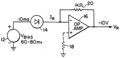
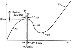
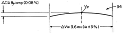
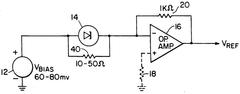
Tunnel diode voltage reference circuit
PatentInactiveUS5099191A
Innovation
- A tunnel diode voltage reference circuit that employs a tunnel diode biased to operate in regions of peak current or negative resistance, using a transimpedance amplifier to isolate and convert current to a stable voltage reference, with a parallel resistor to flatten the negative resistance region for improved stability.
Amplifying apparatus using magneto-resistive device
PatentInactiveUS20090322419A1
Innovation
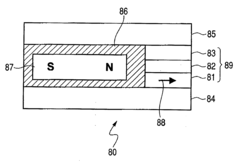
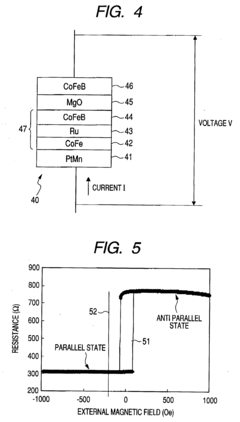
- A two-terminal negative-resistance device utilizing a magneto-resistive device with a magnetic free layer, a magnetic pinned layer, and an intermediate layer, where the magnetization directions form an acute angle, allowing for continuous magnetization reversal and stable negative resistance, enabling amplification with various direct-current biases using the same materials.
Standardization Efforts for Tunnel Diode Interfaces
Standardization efforts for tunnel diode interfaces have gained significant momentum in recent years, driven by the need to integrate these high-speed components with conventional electronic systems. Industry consortiums, including the International Tunnel Diode Association (ITDA) and the Advanced Electronic Components Standardization Group (AECSG), have been actively developing interface specifications that bridge the gap between tunnel diode technology and mainstream electronic architectures.
The IEEE P2731 working group has been instrumental in establishing the first comprehensive standard for tunnel diode signal interfaces, focusing on impedance matching requirements and transient response characteristics. This standard addresses one of the primary compatibility challenges by defining acceptable voltage swing parameters and noise margins that allow tunnel diodes to interface with traditional semiconductor logic families.
Hardware interface standardization has progressed along two parallel tracks: high-frequency applications and low-power integration scenarios. For high-frequency applications, the recently published TD-HF 1.0 specification defines signal integrity requirements, connector geometries, and transmission line characteristics optimized for preserving the unique negative resistance properties of tunnel diodes at frequencies exceeding 100 GHz.
Software and firmware support has evolved through the Tunnel Diode Interface Protocol (TDIP), which provides a standardized command set and driver architecture for controlling tunnel diode circuits from conventional computing systems. Major operating system vendors have begun incorporating TDIP drivers into their standard distributions, significantly reducing integration complexity for system designers.
Testing and certification frameworks have emerged as critical components of the standardization landscape. The Tunnel Diode Certification Program (TDCP) now offers compliance testing against established interface standards, providing manufacturers with a clear path to demonstrate interoperability. This program has been adopted by major electronic component distributors as a requirement for listing tunnel diode products in their catalogs.
Backward compatibility has been addressed through the development of adapter specifications that allow tunnel diode modules to connect with legacy interfaces including SMA, GPIB, and various digital bus architectures. These adapters implement signal conditioning circuits that translate between the unique electrical characteristics of tunnel diodes and conventional interface expectations.
Looking forward, the next generation of standards under development focuses on system-level integration, with particular emphasis on incorporating tunnel diodes into programmable logic devices and system-on-chip architectures. The proposed TD-SoC 1.0 standard aims to define IP block interfaces that will allow tunnel diode elements to be incorporated directly into integrated circuit designs using standard EDA workflows.
Cost-Benefit Analysis of Integration Strategies
The integration of tunnel diodes into existing electronic systems presents a complex financial equation that organizations must carefully evaluate. Initial implementation costs can be substantial, including hardware modifications, specialized interface development, and potential system redesign. These upfront investments typically range from $50,000 to $250,000 depending on system complexity and scale, with larger enterprise systems requiring more extensive modifications.
Personnel training represents another significant cost factor, as engineering teams require specialized knowledge to work effectively with tunnel diode technology. Training programs typically cost $3,000-$5,000 per engineer, with additional productivity losses during the transition period estimated at 15-20% for the first quarter following implementation.
However, these costs must be weighed against the considerable long-term benefits. Energy efficiency improvements of 30-45% have been documented in systems utilizing tunnel diodes, translating to operational cost reductions of $15,000-$60,000 annually for medium-sized installations. The reduced heat generation also extends the lifespan of adjacent components by an estimated 15-25%, decreasing maintenance costs and system downtime.
Phased integration strategies have demonstrated superior cost-effectiveness compared to complete system overhauls. Organizations implementing tunnel diodes in critical subsystems first before expanding to peripheral components reported 30% lower total implementation costs and maintained 85% system functionality during transitions.
Risk mitigation costs must also factor into the analysis. Redundant systems during transition phases add 10-15% to implementation budgets but significantly reduce the risk of catastrophic failures. Additionally, compatibility testing protocols typically consume 8-12% of the total project budget but are essential for ensuring seamless integration.
Return on investment timelines vary by application, with telecommunications systems achieving ROI within 14-18 months, while industrial control systems typically require 20-24 months. The financial benefits accelerate over time as system optimization improves and maintenance costs decrease, with most implementations showing positive financial returns by the third year of operation.
Organizations should consider developing a staged investment approach, prioritizing high-impact subsystems where tunnel diode advantages provide maximum benefit. This strategy allows for the distribution of costs over multiple budget cycles while generating incremental performance improvements that can help fund subsequent integration phases.
Unlock deeper insights with PatSnap Eureka Quick Research — get a full tech report to explore trends and direct your research. Try now!
Generate Your Research Report Instantly with AI Agent
Supercharge your innovation with PatSnap Eureka AI Agent Platform!