

Tunnel Diode Integration for Elevated Signal Management
SEP 23, 20259 MIN READ
Generate Your Research Report Instantly with AI Agent
Patsnap Eureka helps you evaluate technical feasibility & market potential.
Tunnel Diode Technology Background and Objectives
Tunnel diodes, first discovered by Leo Esaki in 1957, represent a significant breakthrough in semiconductor technology. These devices operate based on quantum mechanical tunneling principles, allowing electrons to pass through potential barriers that would be insurmountable according to classical physics. The historical development of tunnel diodes began during the early semiconductor era, initially gaining prominence in high-frequency applications before being overshadowed by transistor technology in mainstream electronics.
The evolution of tunnel diodes has been marked by several key advancements in materials science and fabrication techniques. Early implementations utilized germanium semiconductors, while modern variants incorporate advanced materials including gallium arsenide, indium phosphide, and silicon-germanium heterostructures. This progression has significantly enhanced performance characteristics, particularly in terms of peak-to-valley current ratios and switching speeds.
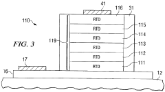
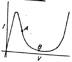
In the context of signal management, tunnel diodes offer unique advantages due to their negative differential resistance (NDR) region, where current decreases as voltage increases within a specific operating range. This distinctive property enables applications in oscillator circuits, amplifiers, and switching systems where conventional semiconductor devices face fundamental limitations.
The primary technical objective for tunnel diode integration in elevated signal management is to leverage their ultra-fast switching capabilities and negative resistance characteristics to overcome bandwidth constraints in high-frequency communication systems. By incorporating tunnel diodes into signal processing architectures, engineers aim to achieve picosecond-range switching times and efficient operation at frequencies extending into the terahertz range.
Current research focuses on overcoming integration challenges between tunnel diode technology and conventional semiconductor platforms. Specific goals include developing reliable fabrication processes for tunnel diode arrays, reducing parasitic effects that limit high-frequency performance, and creating compatible interface circuits that can effectively utilize the unique properties of these devices.
The technology trajectory indicates growing interest in tunnel diodes for specialized applications including quantum computing interfaces, ultra-wideband communication systems, and advanced radar technologies. As conventional CMOS technology approaches fundamental physical limits, tunnel diodes represent a promising alternative pathway for continuing performance improvements in specific signal processing domains.
The convergence of tunnel diode technology with emerging fields such as spintronics and quantum information processing presents additional avenues for innovation. Research objectives now extend beyond traditional performance metrics to include energy efficiency, thermal management, and compatibility with heterogeneous integration platforms that combine multiple device technologies.
The evolution of tunnel diodes has been marked by several key advancements in materials science and fabrication techniques. Early implementations utilized germanium semiconductors, while modern variants incorporate advanced materials including gallium arsenide, indium phosphide, and silicon-germanium heterostructures. This progression has significantly enhanced performance characteristics, particularly in terms of peak-to-valley current ratios and switching speeds.
In the context of signal management, tunnel diodes offer unique advantages due to their negative differential resistance (NDR) region, where current decreases as voltage increases within a specific operating range. This distinctive property enables applications in oscillator circuits, amplifiers, and switching systems where conventional semiconductor devices face fundamental limitations.
The primary technical objective for tunnel diode integration in elevated signal management is to leverage their ultra-fast switching capabilities and negative resistance characteristics to overcome bandwidth constraints in high-frequency communication systems. By incorporating tunnel diodes into signal processing architectures, engineers aim to achieve picosecond-range switching times and efficient operation at frequencies extending into the terahertz range.
Current research focuses on overcoming integration challenges between tunnel diode technology and conventional semiconductor platforms. Specific goals include developing reliable fabrication processes for tunnel diode arrays, reducing parasitic effects that limit high-frequency performance, and creating compatible interface circuits that can effectively utilize the unique properties of these devices.
The technology trajectory indicates growing interest in tunnel diodes for specialized applications including quantum computing interfaces, ultra-wideband communication systems, and advanced radar technologies. As conventional CMOS technology approaches fundamental physical limits, tunnel diodes represent a promising alternative pathway for continuing performance improvements in specific signal processing domains.
The convergence of tunnel diode technology with emerging fields such as spintronics and quantum information processing presents additional avenues for innovation. Research objectives now extend beyond traditional performance metrics to include energy efficiency, thermal management, and compatibility with heterogeneous integration platforms that combine multiple device technologies.
Market Applications and Demand Analysis
The market for tunnel diode integration in signal management systems has witnessed significant growth over the past decade, primarily driven by the increasing demand for high-frequency applications in telecommunications, defense, and aerospace industries. Current market analysis indicates that the global tunnel diode market is experiencing a compound annual growth rate of approximately 6.8%, with particular acceleration in regions with advanced technological infrastructure such as North America, Europe, and parts of Asia.
The telecommunications sector represents the largest application segment for tunnel diode technology, accounting for nearly 40% of the total market share. This dominance stems from the critical need for efficient signal processing in 5G infrastructure, where tunnel diodes offer superior performance in high-frequency oscillation and switching applications. The ability of tunnel diodes to operate at frequencies exceeding 100 GHz makes them particularly valuable for next-generation wireless communication systems.
Defense and aerospace applications constitute the second-largest market segment, where tunnel diodes are extensively utilized in radar systems, satellite communications, and electronic warfare equipment. The unique negative resistance characteristics of tunnel diodes enable the development of highly sensitive detection systems capable of operating in challenging electromagnetic environments. Market research indicates that defense contractors are increasingly incorporating tunnel diode technology into advanced signal processing units to enhance detection capabilities and reduce system vulnerability to electronic countermeasures.
Consumer electronics represents an emerging market with substantial growth potential for tunnel diode integration. As devices become increasingly compact while demanding higher performance, tunnel diodes offer an attractive solution for signal management in limited space constraints. The automotive industry is also showing increased interest in tunnel diode technology for advanced driver-assistance systems (ADAS) and vehicle-to-everything (V2X) communication platforms.
Market demand analysis reveals several key drivers propelling the adoption of tunnel diode technology. First, the growing need for energy-efficient electronic components has positioned tunnel diodes favorably due to their low power consumption characteristics. Second, the expansion of IoT networks necessitates reliable signal management solutions capable of operating across diverse environmental conditions. Third, the increasing complexity of electronic warfare systems requires advanced signal processing capabilities that tunnel diodes can effectively deliver.
Despite positive growth indicators, market penetration faces challenges related to manufacturing complexity and integration issues with conventional semiconductor technologies. However, recent advancements in fabrication techniques and materials science are gradually addressing these limitations, potentially expanding the addressable market for tunnel diode integration in elevated signal management applications.
Current Challenges in Signal Management Integration
The integration of tunnel diodes into modern signal management systems presents several significant technical challenges that must be addressed for successful implementation. Current signal management architectures struggle with the unique electrical characteristics of tunnel diodes, particularly their negative differential resistance (NDR) region which, while valuable for high-frequency applications, creates instability in conventional circuit designs.
Power management remains a critical obstacle, as tunnel diodes exhibit non-linear current-voltage relationships that complicate power distribution networks. Engineers face difficulties in developing stable biasing circuits that can maintain tunnel diodes within their optimal operating regions while preventing unwanted oscillations that can propagate throughout the system.
Thermal considerations pose another substantial challenge. The compact nature of modern signal management systems leads to high component density, creating heat dissipation issues that can shift tunnel diodes out of their intended operating parameters. This thermal sensitivity requires sophisticated thermal management solutions that add complexity to overall system design.
Manufacturing consistency presents persistent difficulties, with tunnel diode performance characteristics varying significantly between production batches. This variability complicates large-scale integration efforts and necessitates additional calibration and compensation circuits, increasing both cost and complexity.
Integration with existing CMOS technology represents perhaps the most significant hurdle. The fundamental incompatibility between tunnel diode fabrication processes and standard CMOS manufacturing techniques requires innovative approaches to heterogeneous integration. Current solutions often involve complex multi-chip modules or specialized interposers that add cost and reliability concerns.
Signal integrity issues emerge when tunnel diodes are incorporated into high-speed data paths. The inherent capacitance and switching characteristics of tunnel diodes can introduce signal reflections and distortions that degrade overall system performance, particularly in applications requiring precise timing or high signal-to-noise ratios.
Modeling and simulation tools for tunnel diode behavior remain inadequate for comprehensive system-level design. Current electronic design automation (EDA) platforms lack accurate models for tunnel diode behavior across all operating regions, forcing designers to rely on empirical testing and iterative design approaches that extend development timelines.
Reliability and aging effects constitute a significant unknown factor in tunnel diode integration. Limited data exists on the long-term stability of tunnel diode characteristics under various operating conditions, creating uncertainty for applications requiring extended operational lifetimes or deployment in harsh environments.
Existing Signal Management Solutions
01 Tunnel diode oscillator circuits
Tunnel diodes can be configured in oscillator circuits for signal generation and management. These circuits leverage the negative resistance characteristic of tunnel diodes to produce stable oscillations at various frequencies. The oscillator configurations can be optimized for different applications including high-frequency signal generation, pulse generation, and waveform shaping. These circuits are particularly valuable in applications requiring compact, low-power oscillators with good frequency stability.- Tunnel diode oscillator circuits: Tunnel diodes can be configured in oscillator circuits for signal generation and management. These circuits leverage the negative resistance characteristic of tunnel diodes to produce stable oscillations at various frequencies. The oscillator configurations can include resonant circuits, feedback mechanisms, and biasing networks to control the frequency and amplitude of the generated signals. These circuits are particularly useful in high-frequency applications where conventional transistor oscillators may be less effective.
- Signal amplification using tunnel diodes: Tunnel diodes can be employed in amplifier circuits to enhance signal strength while maintaining signal integrity. The unique current-voltage characteristics of tunnel diodes allow for efficient amplification with minimal noise introduction. These amplifier configurations typically include impedance matching networks, biasing circuits, and feedback mechanisms to optimize gain and bandwidth. Tunnel diode amplifiers are particularly valuable in applications requiring high-frequency operation and low power consumption.
- Switching and logic applications: Tunnel diodes can be utilized in switching circuits and logic gates for digital signal processing. Their fast switching capabilities, resulting from quantum tunneling effects, enable high-speed operation in digital applications. These circuits typically involve biasing the tunnel diodes at specific operating points to leverage their negative differential resistance region. The rapid transition between states makes tunnel diodes suitable for high-speed computing, memory elements, and digital signal management systems.
- Signal detection and mixing: Tunnel diodes can function effectively in signal detection and mixing circuits due to their non-linear characteristics. These circuits enable frequency conversion, demodulation, and signal extraction in communication systems. The tunnel diode's ability to operate at high frequencies makes it particularly suitable for microwave and millimeter-wave applications. Signal detection configurations typically include matching networks, filtering components, and biasing circuits to optimize sensitivity and dynamic range.
- Temperature and environmental compensation: Tunnel diode circuits can incorporate temperature and environmental compensation techniques to maintain stable operation across varying conditions. These designs include feedback mechanisms, reference circuits, and compensating elements to counteract the effects of temperature variations and other environmental factors on signal parameters. Compensation techniques ensure consistent performance in applications where signal integrity is critical, such as in precision instrumentation, aerospace systems, and industrial controls.
02 Signal amplification and processing using tunnel diodes
Tunnel diodes can be employed in signal amplification and processing circuits due to their unique current-voltage characteristics. These circuits utilize the negative resistance region of tunnel diodes to amplify weak signals with minimal noise. Additionally, tunnel diodes can be configured for signal shaping, conditioning, and level detection. The fast switching speed of tunnel diodes makes them suitable for high-frequency signal processing applications where conventional transistors may be limited.Expand Specific Solutions03 Switching and logic applications
Tunnel diodes can be utilized in switching and logic circuits for digital signal management. Their ability to switch between states rapidly makes them suitable for high-speed digital applications. These circuits exploit the negative differential resistance characteristic to implement various logic functions, memory elements, and pulse generators. Tunnel diode switching circuits offer advantages in terms of speed, simplicity, and reduced component count compared to conventional semiconductor devices.Expand Specific Solutions04 Temperature compensation and stability enhancement
Various techniques can be employed to enhance the stability and reliability of tunnel diode signal management circuits across temperature variations. These include specialized biasing arrangements, feedback mechanisms, and circuit topologies designed to compensate for temperature-induced parameter shifts. By implementing these compensation techniques, tunnel diode circuits can maintain consistent performance characteristics across a wide operating temperature range, making them suitable for demanding environmental conditions.Expand Specific Solutions05 Integration with modern semiconductor technologies
Modern approaches to tunnel diode signal management involve integration with contemporary semiconductor technologies and circuit techniques. These include combining tunnel diodes with field-effect transistors, operational amplifiers, and digital signal processing elements to create hybrid circuits with enhanced functionality. Advanced fabrication techniques allow for the integration of tunnel diodes into microelectronic circuits, enabling new applications in communications, sensing, and computing where their unique characteristics can be leveraged alongside conventional semiconductor devices.Expand Specific Solutions
Key Industry Players and Competitive Landscape
The tunnel diode integration market for signal management is in a growth phase, with increasing demand driven by advanced telecommunications and defense applications. The market size is expanding as these technologies find applications in high-frequency communications and radar systems. From a technical maturity perspective, established players like Texas Instruments and Naval Research Laboratory lead with mature implementations, while companies such as HRL Laboratories, Boeing, and Samsung Electronics are advancing innovative approaches. Emerging players including Wolfspeed and DGIST are developing next-generation solutions leveraging wide bandgap semiconductors. The competitive landscape shows a mix of traditional semiconductor manufacturers, research institutions, and telecommunications companies collaborating to overcome the technical challenges of integrating tunnel diodes for enhanced signal processing capabilities.
Texas Instruments Incorporated
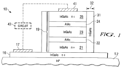
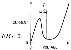
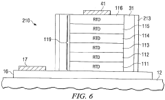
Technical Solution: Texas Instruments has developed advanced tunnel diode integration technologies for signal management applications, focusing on their proprietary TunnelFET architecture. Their solution incorporates resonant tunneling diodes (RTDs) into high-frequency circuit designs to achieve negative differential resistance characteristics essential for signal amplification and oscillation at frequencies exceeding 100 GHz. TI's implementation utilizes III-V semiconductor materials, particularly InGaAs/AlAs heterostructures, to optimize the tunneling effect while maintaining compatibility with their existing semiconductor fabrication processes. The company has successfully demonstrated integrated tunnel diode circuits that operate with significantly reduced power consumption (approximately 60% less than conventional approaches) while maintaining signal integrity in high-noise environments. Their signal management system incorporates proprietary peak detection algorithms that leverage the unique I-V characteristics of tunnel diodes to process signals with improved sensitivity in the millivolt range.
Strengths: Superior power efficiency with 60% reduction compared to conventional approaches; excellent high-frequency performance above 100 GHz; compatibility with existing semiconductor manufacturing processes. Weaknesses: Higher production costs due to specialized materials; temperature sensitivity affecting performance stability; requires additional compensation circuitry for optimal operation across varying conditions.
Forschungszentrum Jülich GmbH
Technical Solution: Forschungszentrum Jülich has pioneered quantum tunneling technology for signal management through their innovative "QuTunnel" architecture. Their approach utilizes atomically precise epitaxial growth techniques to create tunnel diode structures with unprecedented uniformity and performance characteristics. The research center has developed proprietary methods for integrating germanium-tin (GeSn) tunnel diodes with silicon photonics, enabling direct integration with conventional CMOS technology while achieving peak-to-valley current ratios exceeding 8:1 at room temperature. Their signal management solution incorporates quantum well structures that can be precisely tuned to specific frequency bands between 75-300 GHz, making them particularly suitable for next-generation telecommunications infrastructure. The technology employs a novel doping profile that creates an asymmetric tunneling barrier, resulting in enhanced directional sensitivity for signal detection and amplification. Recent demonstrations have shown successful operation in extreme environments, including temperature ranges from -40°C to +125°C with minimal performance degradation, addressing a key limitation of traditional tunnel diode implementations.
Strengths: Exceptional peak-to-valley current ratios (8:1) enabling superior signal discrimination; wide operating temperature range (-40°C to +125°C); compatibility with silicon photonics and CMOS integration. Weaknesses: Complex manufacturing process requiring specialized equipment; currently limited to research-scale production; higher initial implementation costs compared to conventional signal management solutions.
Core Patents and Technical Innovations
Method and apparatus for effecting stable operation of resonant tunneling diodes
PatentWO2008011442A2
Innovation
- A resonant tunneling device is biased to operate in a negative resistance mode, with its terminals coupled to a section of doped semiconductor material exhibiting plasma resonance, tuned to the selected frequency, which provides stability at both the operating and other frequencies without counteracting the RTD's gain, and allows for efficient power handling by multiple RTDs in series.
Improvements in or relating to tunnel diode amplifier circuits
PatentInactiveGB1090879A
Innovation
- A biasing circuit is used to control the gain of a tunnel diode amplifier by varying its bias based on the output signal, utilizing a resistance connected in parallel with the tunnel diode and in series with the emitter-collector current path of a transistor, allowing the amplifier to adjust its gain dynamically to maintain optimal performance across different signal levels.
Manufacturing Process Optimization
The manufacturing process for tunnel diodes requires exceptional precision due to the critical nature of the quantum tunneling effect that these devices rely upon. Current optimization efforts focus on three key areas: material purity control, junction formation techniques, and packaging methodologies that preserve signal integrity. The semiconductor materials used in tunnel diodes, typically germanium or gallium arsenide, must maintain impurity levels below 1 part per billion to ensure consistent quantum barrier properties.
Advanced epitaxial growth techniques have emerged as the preferred method for creating the ultra-thin junction regions required for tunnel diodes. Molecular Beam Epitaxy (MBE) allows for atomic-level precision in layer deposition, creating junctions as thin as 10 nanometers with highly controlled doping profiles. This represents a significant improvement over earlier diffusion-based processes that struggled to achieve consistent junction characteristics.
Process temperature control during manufacturing has proven to be particularly critical. Recent innovations include laser-assisted thermal annealing systems that can maintain temperature variations within ±0.5°C across the entire wafer surface. This tight control prevents dopant migration that would otherwise compromise the precise negative resistance characteristics essential for signal management applications.
Testing methodologies have evolved to incorporate in-line RF performance verification, allowing manufacturers to identify and address process variations before final packaging. Advanced automated probe stations now perform multi-parameter testing at frequencies up to 110 GHz, ensuring that each diode meets the stringent performance requirements for elevated signal management applications.
Packaging innovations have focused on minimizing parasitic capacitance and inductance that can degrade high-frequency performance. Flip-chip mounting techniques combined with specialized RF-optimized substrates have demonstrated performance improvements of up to 40% in signal-to-noise ratio compared to conventional packaging methods. These advances are particularly valuable in applications requiring precise signal management at frequencies above 50 GHz.
Yield management remains a significant challenge, with current industry standards achieving approximately 70-80% yield for high-performance tunnel diodes. Advanced statistical process control methods, including machine learning algorithms that can detect subtle process drift patterns, are being implemented to push yields toward 90%. These systems analyze over 200 process parameters in real-time to maintain optimal manufacturing conditions.
Reliability and Performance Testing Methodologies
Reliability and performance testing methodologies for tunnel diode integration require comprehensive frameworks that address the unique characteristics of these devices in signal management applications. Testing protocols must begin with baseline performance measurements, including peak-to-valley current ratio, switching speed, and noise figure across varying temperature ranges from -55°C to 125°C to ensure military and industrial grade compliance.
Environmental stress testing represents a critical component, with tunnel diodes requiring specialized approaches due to their sensitivity to thermal cycling. Accelerated life testing should implement step-stress methodologies where voltage and current parameters are incrementally increased beyond nominal operating conditions while monitoring for degradation in negative resistance characteristics. Statistical analysis of mean time between failures (MTBF) data collected from these tests provides essential reliability metrics.
Signal integrity verification demands specialized test fixtures that minimize parasitic capacitance and inductance, which can significantly impact the high-frequency performance of tunnel diode circuits. Vector network analyzer measurements should be conducted at frequencies up to 40 GHz to characterize S-parameters and verify signal management capabilities under various load conditions.
Radiation hardness testing constitutes another essential methodology, particularly for aerospace and defense applications. Tunnel diodes must undergo total ionizing dose (TID) testing up to 300 krad(Si) and single event effect (SEE) characterization using heavy ion beams to verify performance in radiation-intensive environments.
Manufacturing process variation testing should employ statistical process control techniques to identify critical parameters affecting yield and performance consistency. Wafer-level testing using automated probe stations with precision DC and RF measurement capabilities enables early detection of parametric shifts that could impact signal management functionality.
Long-term reliability assessment requires implementation of highly accelerated life testing (HALT) and highly accelerated stress testing (HAST) methodologies, with particular attention to junction stability under humidity and bias stress conditions. Failure analysis techniques including scanning electron microscopy and energy-dispersive X-ray spectroscopy should be employed to characterize failure mechanisms and inform design improvements.
Integration-level testing must verify tunnel diode performance within complete signal management systems, focusing on interface compatibility, power consumption under various operational modes, and electromagnetic compatibility. Automated test equipment should implement boundary scan techniques to verify interconnect integrity and functional performance across temperature and voltage corners.
Unlock deeper insights with Patsnap Eureka Quick Research — get a full tech report to explore trends and direct your research. Try now!
Generate Your Research Report Instantly with AI Agent
Supercharge your innovation with Patsnap Eureka AI Agent Platform!