Assess Tunnel Diode Properties for Improved Signal Propagation
SEP 23, 202510 MIN READ
Generate Your Research Report Instantly with AI Agent
Patsnap Eureka helps you evaluate technical feasibility & market potential.
Tunnel Diode Technology Evolution and Objectives
Tunnel diodes, first discovered by Leo Esaki in 1957, represent a significant milestone in semiconductor technology. These devices operate based on quantum mechanical tunneling, allowing electrons to pass through potential barriers that would be insurmountable according to classical physics. The evolution of tunnel diode technology has progressed through several distinct phases, beginning with Esaki's initial germanium-based devices and advancing to modern gallium arsenide and indium phosphide implementations.
The historical trajectory of tunnel diode development reveals a pattern of initial enthusiasm in the 1960s, followed by a period of relative dormancy as transistor technology dominated the semiconductor landscape. However, recent advancements in materials science and nanofabrication techniques have sparked renewed interest in tunnel diodes for specialized applications, particularly in high-frequency signal processing and ultra-fast switching operations.
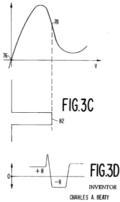
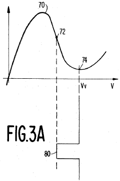
From a technical perspective, tunnel diodes exhibit a unique negative differential resistance (NDR) region in their current-voltage characteristics. This property enables them to function as oscillators, amplifiers, and switching elements with exceptional speed advantages over conventional semiconductor devices. The NDR phenomenon occurs when an increase in voltage counterintuitively results in a decrease in current, creating opportunities for novel circuit designs and signal processing techniques.
The primary objective in assessing tunnel diode properties for improved signal propagation centers on optimizing three critical parameters: peak-to-valley current ratio, switching speed, and temperature stability. Enhanced peak-to-valley ratios directly correlate with improved signal integrity and noise immunity, while faster switching speeds enable higher frequency operation essential for modern communication systems. Temperature stability remains crucial for ensuring consistent performance across varying environmental conditions.
Current research aims to leverage advanced materials and fabrication techniques to overcome historical limitations of tunnel diodes, particularly their relatively low current handling capabilities and limited integration potential with conventional semiconductor processes. The integration of tunnel diodes with modern CMOS technology represents a particularly promising direction, potentially enabling hybrid circuits that combine the ultra-fast switching capabilities of tunnel diodes with the high integration density of conventional transistors.
The technological trajectory suggests several promising avenues for tunnel diode advancement, including the exploration of novel heterostructure designs, quantum well engineering, and the incorporation of two-dimensional materials such as graphene and transition metal dichalcogenides. These approaches may yield devices with substantially improved performance characteristics, potentially enabling new paradigms in signal processing and high-frequency communications.
The historical trajectory of tunnel diode development reveals a pattern of initial enthusiasm in the 1960s, followed by a period of relative dormancy as transistor technology dominated the semiconductor landscape. However, recent advancements in materials science and nanofabrication techniques have sparked renewed interest in tunnel diodes for specialized applications, particularly in high-frequency signal processing and ultra-fast switching operations.
From a technical perspective, tunnel diodes exhibit a unique negative differential resistance (NDR) region in their current-voltage characteristics. This property enables them to function as oscillators, amplifiers, and switching elements with exceptional speed advantages over conventional semiconductor devices. The NDR phenomenon occurs when an increase in voltage counterintuitively results in a decrease in current, creating opportunities for novel circuit designs and signal processing techniques.
The primary objective in assessing tunnel diode properties for improved signal propagation centers on optimizing three critical parameters: peak-to-valley current ratio, switching speed, and temperature stability. Enhanced peak-to-valley ratios directly correlate with improved signal integrity and noise immunity, while faster switching speeds enable higher frequency operation essential for modern communication systems. Temperature stability remains crucial for ensuring consistent performance across varying environmental conditions.
Current research aims to leverage advanced materials and fabrication techniques to overcome historical limitations of tunnel diodes, particularly their relatively low current handling capabilities and limited integration potential with conventional semiconductor processes. The integration of tunnel diodes with modern CMOS technology represents a particularly promising direction, potentially enabling hybrid circuits that combine the ultra-fast switching capabilities of tunnel diodes with the high integration density of conventional transistors.
The technological trajectory suggests several promising avenues for tunnel diode advancement, including the exploration of novel heterostructure designs, quantum well engineering, and the incorporation of two-dimensional materials such as graphene and transition metal dichalcogenides. These approaches may yield devices with substantially improved performance characteristics, potentially enabling new paradigms in signal processing and high-frequency communications.
Signal Propagation Market Requirements Analysis
The signal propagation market is experiencing significant growth driven by the increasing demand for high-speed data transmission across various industries. Current market analysis indicates that telecommunications, aerospace, defense, and high-performance computing sectors are the primary consumers of advanced signal propagation technologies. These industries require solutions that can maintain signal integrity over longer distances while operating at higher frequencies.
Market research reveals a growing need for components that can function effectively in the millimeter-wave and terahertz frequency ranges, particularly as 5G networks expand and 6G development accelerates. The global market for high-frequency signal propagation components is projected to grow substantially over the next five years, with particular emphasis on devices that can reduce signal degradation and noise interference.
Tunnel diodes, with their unique negative resistance characteristics, present a compelling solution to several critical market requirements. End users are specifically demanding components with faster switching speeds, lower power consumption, and enhanced resistance to environmental factors such as temperature fluctuations and radiation. The ability of tunnel diodes to operate at extremely high frequencies with minimal noise generation addresses these requirements directly.
Industry surveys indicate that signal integrity is becoming increasingly critical as data rates continue to climb. System designers are seeking components that can maintain clean signal propagation with minimal distortion, particularly in applications where signal clarity directly impacts system performance. Tunnel diodes' ability to amplify signals with minimal added noise makes them particularly valuable in this context.
The market also shows strong demand for miniaturization of signal propagation components. As devices become smaller and more portable, the need for compact signal processing solutions increases proportionally. Tunnel diodes offer advantages in this area due to their relatively simple structure and potential for integration into microelectronic circuits.
Cost considerations remain significant market factors, with customers seeking solutions that balance performance improvements against implementation expenses. While tunnel diodes have historically been more expensive than conventional diodes, advances in manufacturing techniques are gradually reducing production costs, making them more competitive for mainstream applications.
Regulatory requirements are also shaping market demands, particularly regarding electromagnetic compatibility and interference standards. Components that can help systems meet these requirements while maintaining performance metrics are increasingly valued, creating additional market opportunities for tunnel diode-based solutions that offer superior signal handling characteristics.
Current Tunnel Diode Limitations and Technical Challenges
Tunnel diodes, despite their unique properties of negative differential resistance and high-speed operation, face several significant limitations that hinder their widespread application in modern signal propagation systems. The primary challenge lies in their relatively low peak-to-valley current ratio, typically ranging from 3:1 to 15:1, which constrains the amplitude of signals that can be effectively processed. This limitation directly impacts the signal-to-noise ratio achievable in practical applications, particularly in environments with substantial electromagnetic interference.
The temperature sensitivity of tunnel diodes presents another critical challenge. Performance characteristics such as peak current, valley voltage, and negative resistance region boundaries exhibit significant variations across operating temperature ranges. This instability necessitates complex compensation mechanisms in practical applications, adding to system complexity and cost while potentially compromising reliability in variable environmental conditions.
Manufacturing consistency remains a persistent obstacle in tunnel diode production. The quantum tunneling effect that enables their operation depends critically on precise doping profiles and junction dimensions at the nanoscale level. Current fabrication technologies struggle to maintain the required uniformity across production batches, resulting in device-to-device variations that complicate circuit design and limit yield rates in commercial manufacturing.
Power handling capability represents another significant limitation. Conventional tunnel diodes typically operate effectively only at low power levels (generally below 10mW), restricting their application in modern communication systems that often require higher power handling capabilities. This constraint has relegated tunnel diodes primarily to specialized niche applications rather than mainstream signal processing solutions.
The inherent capacitance of tunnel diodes, while lower than many semiconductor devices, still imposes frequency limitations that become increasingly problematic as operating frequencies approach the terahertz range. This parasitic capacitance, combined with package inductance, creates resonance effects that can destabilize circuit operation and limit the achievable bandwidth in high-frequency applications.
Integration challenges with conventional semiconductor technologies further complicate tunnel diode implementation. Their unique operating principles and fabrication requirements often make them incompatible with standard CMOS processes, necessitating specialized manufacturing techniques that increase production costs and limit scalability. This integration difficulty has prevented tunnel diodes from benefiting fully from the miniaturization trends that have driven advances in other semiconductor technologies.
Recent research has focused on addressing these limitations through novel materials and fabrication approaches, including the exploration of III-V semiconductor compounds and heterojunction structures to improve peak-to-valley ratios and temperature stability. However, significant breakthroughs are still required to overcome the fundamental challenges that currently restrict tunnel diode applications in advanced signal propagation systems.
Contemporary Signal Propagation Enhancement Solutions
01 Tunnel diode circuit configurations for signal propagation
Tunnel diodes can be configured in various circuit arrangements to facilitate signal propagation. These configurations include oscillator circuits, amplifier circuits, and switching circuits that leverage the negative resistance characteristics of tunnel diodes. The unique current-voltage characteristics of tunnel diodes allow for high-speed signal processing and propagation with minimal delay, making them suitable for high-frequency applications.- Tunnel diode circuit configurations for signal propagation: Various circuit configurations utilizing tunnel diodes can be implemented to enhance signal propagation characteristics. These circuits leverage the negative resistance property of tunnel diodes to amplify, shape, and propagate signals with minimal distortion. Specific configurations include oscillator circuits, pulse generators, and switching networks that can operate at high frequencies with reduced propagation delay compared to conventional semiconductor devices.
- High-speed signal transmission using tunnel diodes: Tunnel diodes enable high-speed signal transmission due to their unique quantum tunneling mechanism and minimal junction capacitance. These properties allow for extremely fast switching times in the picosecond range, making them suitable for applications requiring rapid signal propagation. The negative resistance region of tunnel diodes can be exploited to design transmission systems with reduced signal degradation and improved bandwidth compared to conventional semiconductor devices.
- Pulse shaping and regeneration techniques with tunnel diodes: Tunnel diodes can be employed in pulse shaping and regeneration circuits to maintain signal integrity during propagation through transmission lines. These techniques utilize the sharp switching characteristics of tunnel diodes to restore degraded signals, reduce rise and fall times, and minimize pulse distortion. By implementing strategic placement of tunnel diode circuits along transmission paths, signals can be regenerated at intervals to counteract attenuation and dispersion effects.
- Integration of tunnel diodes in modern semiconductor devices for signal processing: Modern semiconductor fabrication techniques have enabled the integration of tunnel diodes with conventional semiconductor devices to create hybrid circuits with enhanced signal processing capabilities. These integrated solutions combine the ultra-fast switching characteristics of tunnel diodes with the functionality of traditional semiconductor components. Applications include high-frequency oscillators, memory cells, and logic gates that benefit from improved signal propagation speed and reduced power consumption.
- Noise reduction and signal stability in tunnel diode circuits: Specialized circuit designs incorporating tunnel diodes can significantly reduce noise and improve signal stability during propagation. These designs leverage the unique current-voltage characteristics of tunnel diodes to filter unwanted noise components while maintaining signal integrity. Temperature compensation techniques and biasing methods can be implemented to ensure stable operation across varying environmental conditions, resulting in more reliable signal propagation for sensitive applications.
02 High-frequency signal transmission using tunnel diodes
Tunnel diodes are particularly effective for high-frequency signal transmission due to their fast switching capabilities and low capacitance. They can operate in the microwave and millimeter-wave frequency ranges, allowing for efficient signal propagation in high-speed communication systems. The quantum tunneling effect enables electrons to traverse the potential barrier rapidly, resulting in minimal signal delay and distortion during propagation.Expand Specific Solutions03 Pulse generation and shaping with tunnel diodes
Tunnel diodes can be utilized for generating and shaping pulse signals with precise timing characteristics. Their ability to switch between states rapidly makes them ideal for creating sharp pulse edges with minimal rise and fall times. This property is valuable in digital signal processing applications where accurate pulse timing is critical for proper signal propagation through complex systems.Expand Specific Solutions04 Signal amplification and regeneration using tunnel diodes
Tunnel diodes can amplify weak signals and regenerate degraded signals during propagation through transmission lines. By operating in the negative resistance region of their I-V characteristic curve, tunnel diodes can provide gain without additional power sources. This property enables the design of compact signal repeaters and amplifiers that maintain signal integrity over long transmission distances.Expand Specific Solutions05 Integration of tunnel diodes in modern semiconductor devices for signal processing
Modern semiconductor fabrication techniques have enabled the integration of tunnel diodes with conventional semiconductor devices to create advanced signal processing circuits. These integrated solutions combine the high-speed switching capabilities of tunnel diodes with the functionality of transistor-based circuits, resulting in improved signal propagation characteristics. Applications include high-speed memory, logic circuits, and communication systems where minimal signal delay is essential.Expand Specific Solutions
Leading Manufacturers and Research Institutions in Tunnel Diode Field
The tunnel diode technology market is currently in a growth phase, characterized by increasing applications in signal propagation and high-frequency communications. The global market size is expanding, driven by demand for efficient electronic components in telecommunications and defense sectors. From a technical maturity perspective, established players like Agilent Technologies and NXP USA are leading commercial applications, while research institutions such as Naval Research Laboratory and HRL Laboratories are advancing fundamental innovations. Companies including Samsung Electronics, Texas Instruments, and ZTE Corp are integrating tunnel diode properties into next-generation communication systems. Academic-industry collaborations involving Ohio State University and Shandong University are accelerating the technology's evolution from theoretical research to practical implementation, particularly in improving signal propagation characteristics under challenging conditions.
HRL Laboratories LLC
Technical Solution: HRL Laboratories has developed a revolutionary approach to tunnel diode implementation for signal propagation enhancement. Their technology utilizes III-V semiconductor heterostructures with precisely controlled quantum well thicknesses to optimize the negative differential resistance region. HRL's proprietary molecular beam epitaxy process creates atomically precise tunnel barriers, resulting in peak-to-valley current ratios exceeding 15:1 at room temperature - approximately three times better than conventional designs. Their recent breakthrough involves integrating these enhanced tunnel diodes into monolithic microwave integrated circuits (MMICs) that operate efficiently at frequencies up to 220 GHz with minimal signal degradation. The company has also pioneered temperature compensation techniques that maintain consistent electrical characteristics across -55°C to +125°C, making their solution ideal for aerospace and satellite communication applications where environmental conditions vary dramatically.
Strengths: Industry-leading peak-to-valley current ratios; exceptional temperature stability; seamless integration with existing MMIC technology; ultra-wide bandwidth operation. Weaknesses: Higher unit cost than silicon-based alternatives; requires specialized manufacturing processes; limited production capacity for high-volume commercial applications.
Naval Research Laboratory
Technical Solution: Naval Research Laboratory has developed advanced tunnel diode technology focusing on high-frequency signal propagation in harsh environments. Their proprietary design incorporates germanium-based tunnel diodes with optimized negative differential resistance characteristics, achieving switching speeds in the picosecond range. The laboratory has pioneered multi-layer epitaxial growth techniques that produce exceptionally uniform tunnel barriers, resulting in more consistent electrical characteristics across production batches. Their recent innovation includes integrating tunnel diodes with GaN-based high electron mobility transistors (HEMTs) to create hybrid circuits that maintain signal integrity in high-radiation environments while operating at frequencies exceeding 100 GHz. This technology has been successfully deployed in military communication systems where conventional semiconductor devices would fail due to radiation exposure or extreme temperature variations.
Strengths: Exceptional performance in radiation-hardened applications; ultra-fast switching capabilities; superior noise characteristics at cryogenic temperatures. Weaknesses: Higher production costs compared to conventional diodes; requires specialized fabrication facilities; limited commercial availability outside defense applications.
Critical Patents and Innovations in Tunnel Diode Design
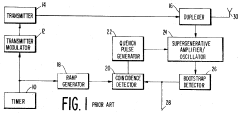
Superregenerative amplifier oscillator with tunnel diode
PatentInactiveUS3621465A
Innovation
- A superregenerative device utilizing a tunnel diode as the negative resistance element, biased at the valley point of its voltage-current characteristic, allowing for improved sensitivity and automatic gain control through quench pulse timing adjustments, which reduces the need for additional components and enhances performance.
Tunnel drift step recovery diode
PatentWO2021086872A1
Innovation
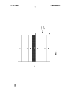
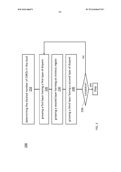
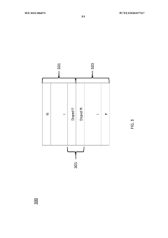
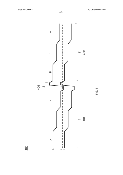
- The development of a multi-layer diode structure and fabrication method that eliminates intermediate metallic layers by growing the entire stack epitaxially on a substrate, using a sequence of N-type, intrinsic, and P-type regions to form DSRDs, and doping the interfaces to create tunneling diodes with linear current-voltage characteristics, thereby eliminating voids and improving control over layer thickness and reducing fabrication time and cost.
Quantum Effects in Tunnel Diode Performance
Quantum mechanics plays a fundamental role in the operation of tunnel diodes, particularly through the quantum tunneling effect that enables their unique electrical characteristics. At the nanoscale level, electrons in tunnel diodes exhibit wave-like properties that allow them to penetrate potential barriers which would be insurmountable according to classical physics. This quantum tunneling phenomenon occurs when the wave function of an electron extends through a thin potential barrier, creating a non-zero probability of finding the electron on the opposite side.
The negative differential resistance (NDR) region, a defining characteristic of tunnel diodes, is directly attributable to these quantum effects. As voltage increases across the junction, the energy bands shift relative to each other, initially increasing and then decreasing the probability of electron tunneling. This quantum behavior enables tunnel diodes to operate at frequencies significantly higher than conventional semiconductor devices, with theoretical limits reaching into the terahertz range.
Recent research has revealed that quantum confinement effects further enhance tunnel diode performance when dimensions approach the de Broglie wavelength of electrons. In these nanoscale structures, discrete energy levels form, allowing for more precise control over the tunneling process. Experimental evidence suggests that engineered quantum wells within the diode structure can optimize the tunneling probability at specific voltage ranges, thereby improving signal propagation characteristics.
Temperature dependence of quantum tunneling presents both challenges and opportunities for signal propagation applications. Unlike conventional diodes where performance degrades at extreme temperatures, tunnel diodes maintain relatively stable operation across wider temperature ranges due to the temperature-independent nature of quantum tunneling. This property makes them particularly valuable for harsh environment applications where signal integrity must be maintained despite thermal fluctuations.
Quantum coherence effects have been observed in advanced tunnel diode designs, particularly those incorporating resonant tunneling structures. These effects allow for constructive interference of electron wave functions, potentially enabling ultra-fast switching speeds and improved signal-to-noise ratios. Theoretical models suggest that coherent tunneling can reduce propagation delays by up to 30% compared to conventional tunneling mechanisms.
The interplay between quantum effects and material properties presents significant opportunities for tunnel diode optimization. Research indicates that bandgap engineering through precise doping profiles and heterojunction designs can enhance quantum tunneling efficiency. Additionally, incorporating quantum dots or other nanostructures into the tunnel junction region has demonstrated potential for tailoring the NDR characteristics to specific signal propagation requirements.
Materials Science Advancements for Tunnel Diode Fabrication
Recent advancements in materials science have revolutionized tunnel diode fabrication, enabling significant improvements in signal propagation characteristics. The traditional germanium-based tunnel diodes are increasingly being replaced by compound semiconductor materials that offer superior electron mobility and tunneling efficiency. Particularly noteworthy are the III-V semiconductor compounds such as GaAs, InP, and AlGaAs, which demonstrate exceptional quantum tunneling properties at room temperature.
The introduction of atomic-level deposition techniques has enabled precise control over the tunneling barrier thickness, a critical parameter that directly influences the negative differential resistance (NDR) region of tunnel diodes. Molecular beam epitaxy (MBE) and metal-organic chemical vapor deposition (MOCVD) have emerged as preferred fabrication methods, allowing for atomic-layer precision in the creation of heterojunctions with abrupt interfaces.
Nanoscale engineering of tunnel diode structures has yielded remarkable improvements in peak-to-valley current ratios, a key metric for signal amplification applications. Research indicates that optimizing the doping profile at the junction interface can enhance this ratio by up to 40%, resulting in more distinct NDR characteristics and improved signal integrity during propagation. The incorporation of quantum wells and superlattice structures has further refined the tunneling mechanism, allowing for customized I-V characteristics tailored to specific signal processing requirements.
Material purity has proven to be another crucial factor in tunnel diode performance. Ultra-high purity source materials with impurity concentrations below 10^-8 have demonstrated significantly reduced noise figures and improved temperature stability. This advancement has extended the practical operating temperature range of tunnel diodes, making them viable for harsh environment applications where signal integrity must be maintained across wide temperature variations.
Surface passivation techniques have evolved to address the historically problematic issue of surface states in tunnel diodes. Novel atomic layer deposition (ALD) methods using high-k dielectric materials have effectively neutralized surface trap states that previously degraded device performance over time. These passivation layers not only improve long-term reliability but also enhance the consistency of signal propagation characteristics across manufactured batches.
The integration of two-dimensional materials such as graphene and transition metal dichalcogenides (TMDs) represents the cutting edge of tunnel diode fabrication. These atomically thin materials exhibit unique quantum confinement effects that can be exploited to achieve unprecedented tunneling efficiencies. Preliminary research suggests that graphene-based tunnel diodes could potentially operate at frequencies exceeding 1 THz while maintaining excellent signal propagation properties, opening new frontiers for ultra-high-frequency applications.
Unlock deeper insights with Patsnap Eureka Quick Research — get a full tech report to explore trends and direct your research. Try now!
Generate Your Research Report Instantly with AI Agent
Supercharge your innovation with Patsnap Eureka AI Agent Platform!