Leverage Tunnel Diode for Noteworthy Signal Enhancement
SEP 23, 202510 MIN READ
Generate Your Research Report Instantly with AI Agent
Patsnap Eureka helps you evaluate technical feasibility & market potential.
Tunnel Diode Technology Background and Objectives
Tunnel diodes, first discovered by Leo Esaki in 1957, represent a significant milestone in semiconductor technology. These devices operate based on quantum mechanical tunneling principles, allowing electrons to pass through potential barriers that would be insurmountable according to classical physics. The historical evolution of tunnel diodes began with germanium-based devices, later expanding to include gallium arsenide and other compound semiconductor materials that offered improved performance characteristics.
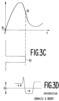
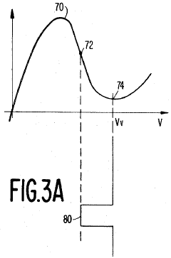
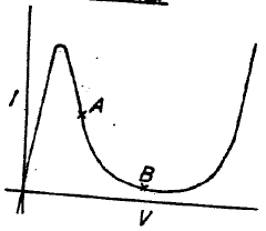
The fundamental operating principle of tunnel diodes centers on their negative differential resistance (NDR) region, where current decreases as voltage increases within a specific operating range. This unique property distinguishes tunnel diodes from conventional semiconductor devices and forms the basis for their signal enhancement capabilities. The NDR characteristic enables tunnel diodes to function as amplifiers, oscillators, and switching elements with exceptional speed advantages.
Technical evolution in this field has followed several distinct phases, beginning with basic research in quantum tunneling phenomena, followed by early device fabrication in the 1960s, integration attempts in the 1970s, and a period of relative dormancy before renewed interest emerged with the advancement of nanotechnology and high-frequency applications in the 1990s and beyond.
Current technological trends indicate growing interest in leveraging tunnel diodes for signal enhancement applications, particularly in high-frequency communications, ultra-sensitive detection systems, and quantum computing interfaces. The ability of tunnel diodes to operate with minimal noise at high frequencies makes them particularly valuable for weak signal amplification scenarios where conventional amplifiers struggle to maintain adequate signal-to-noise ratios.
The primary technical objectives for tunnel diode implementation in signal enhancement include: improving fabrication consistency to ensure reliable NDR characteristics; developing integration methodologies compatible with modern semiconductor manufacturing processes; optimizing operational stability across varying environmental conditions; and creating standardized design frameworks that allow engineers to incorporate tunnel diode elements into complex signal processing chains.
Achieving these objectives would enable significant advancements in several critical application domains, including space communications where weak signal detection is paramount, quantum information processing where minimal signal distortion is essential, and next-generation wireless systems requiring efficient operation at extremely high frequencies.
The renewed focus on tunnel diodes also aligns with broader industry trends toward energy-efficient electronics, as these devices can potentially operate with lower power requirements than conventional amplification technologies while delivering comparable or superior performance in specific applications. This energy efficiency aspect represents an important secondary objective in the ongoing development of tunnel diode technology for signal enhancement purposes.
Market Applications and Demand Analysis
The tunnel diode market is experiencing a significant resurgence, particularly in signal enhancement applications across multiple industries. Current market analysis indicates growing demand for high-frequency signal processing solutions in telecommunications, aerospace, and defense sectors where conventional amplification technologies face limitations in noise performance and power efficiency.
The global market for advanced signal enhancement technologies is projected to reach $12.5 billion by 2027, with tunnel diode-based solutions potentially capturing a growing segment of this market. This growth is primarily driven by the increasing need for reliable signal processing in harsh environments and applications requiring minimal power consumption.
Telecommunications infrastructure represents the largest current market segment, where tunnel diodes offer unique advantages in receiver front-ends and signal conditioning circuits. The rollout of 5G networks has created particular demand for components capable of operating efficiently at millimeter-wave frequencies where tunnel diodes demonstrate superior performance characteristics compared to conventional semiconductor devices.
Aerospace and defense applications constitute another significant market segment, valued at approximately $3.2 billion annually. In these applications, tunnel diodes are increasingly deployed in radar systems, electronic warfare equipment, and satellite communications where their radiation hardness and high-speed switching capabilities provide critical advantages.
Medical equipment manufacturers have also shown renewed interest in tunnel diode technology for signal enhancement in diagnostic imaging systems. The market for advanced medical imaging equipment is growing at 7.3% annually, with particular emphasis on improving signal-to-noise ratios in portable and low-power devices where tunnel diodes excel.
Consumer electronics represents an emerging opportunity, particularly in specialized applications requiring high-frequency operation with minimal power consumption. While currently a smaller segment, industry analysts predict substantial growth potential as manufacturers seek differentiation through improved signal processing capabilities in next-generation devices.
The industrial automation sector has demonstrated increasing demand for robust signal enhancement solutions in environments with significant electromagnetic interference. Tunnel diode-based signal conditioning circuits are gaining traction in factory automation systems, process control equipment, and industrial IoT applications where signal integrity is paramount.
Regional analysis reveals that North America currently leads in tunnel diode adoption for signal enhancement applications, followed by Asia-Pacific where rapid infrastructure development and manufacturing growth are driving increased implementation. European markets show steady growth, particularly in specialized industrial and medical applications requiring precise signal processing capabilities.
Current State and Technical Challenges
Tunnel diodes, also known as Esaki diodes, have experienced a resurgence of interest in recent years for signal enhancement applications. The current global landscape shows significant advancements in tunnel diode technology, with research centers in the United States, Japan, and Europe leading development efforts. Recent breakthroughs in semiconductor fabrication techniques have enabled the production of tunnel diodes with improved performance characteristics, including higher peak-to-valley current ratios and enhanced frequency response.
Despite these advancements, several technical challenges persist in leveraging tunnel diodes for signal enhancement. The primary limitation remains the difficulty in achieving consistent manufacturing processes that produce uniform electrical characteristics across large batches. The quantum tunneling effect, which is the fundamental operating principle of these devices, is highly sensitive to atomic-level variations in the semiconductor junction, making mass production with predictable performance parameters challenging.
Temperature sensitivity presents another significant hurdle, as tunnel diodes exhibit considerable drift in their operating points with temperature fluctuations. This instability complicates their integration into systems requiring consistent performance across varying environmental conditions. Current research indicates that temperature compensation circuits can mitigate this issue, but at the cost of increased complexity and power consumption.
Integration with modern CMOS technology represents a substantial technical barrier. While tunnel diodes offer exceptional high-frequency performance and low noise characteristics, their compatibility with standard semiconductor manufacturing processes remains limited. This incompatibility increases production costs and restricts widespread adoption in commercial signal processing applications.
Power handling capability is another constraint, as tunnel diodes typically operate at relatively low power levels. This limitation narrows their application scope, particularly in scenarios requiring signal enhancement for high-power transmissions. Research teams at several universities have demonstrated promising results with parallel configurations to increase power handling, though these solutions introduce additional complexity in matching networks.
The geographical distribution of tunnel diode technology development shows concentration in specific regions. Japan maintains historical leadership in tunnel diode research, with companies like Hitachi and NEC continuing development. In the United States, research institutions including MIT and Stanford University are exploring novel applications in quantum computing and ultra-sensitive detection systems. European efforts are primarily centered in Germany and France, focusing on integration with existing communication infrastructure.
Recent publications indicate emerging interest in tunnel diode applications for 5G and future 6G communication systems, where their unique negative resistance characteristics could enable more efficient signal amplification at millimeter-wave frequencies. However, scaling these laboratory demonstrations to commercial viability remains a significant challenge that will require coordinated efforts across academic and industrial research communities.
Current Signal Enhancement Solutions
01 Tunnel diode circuit configurations for signal amplification
Tunnel diodes can be configured in specific circuit arrangements to enhance signal strength. These configurations leverage the negative resistance characteristics of tunnel diodes to amplify weak signals. Various circuit topologies including series and parallel arrangements with passive components optimize the signal-to-noise ratio and improve overall signal quality. These configurations are particularly effective for high-frequency applications where conventional amplifiers may struggle.- Tunnel diode circuit configurations for signal amplification: Tunnel diodes can be configured in specific circuit arrangements to enhance signal amplification. These configurations leverage the negative resistance characteristics of tunnel diodes to amplify weak signals. Various circuit topologies include differential amplifiers, oscillator circuits, and multi-stage amplification systems that can significantly improve signal-to-noise ratios in electronic systems.
- Frequency enhancement and oscillation techniques: Tunnel diodes can be utilized for frequency enhancement and stable oscillation generation. By exploiting the negative resistance region of tunnel diodes, high-frequency oscillations can be maintained with minimal components. These techniques enable signal enhancement in microwave applications, frequency conversion, and high-speed switching circuits where conventional transistors may be limited by parasitic capacitances.
- Temperature compensation and stability improvements: Methods for improving tunnel diode signal enhancement through temperature compensation and stability control mechanisms. These approaches involve specialized biasing techniques, feedback networks, and material selection to maintain consistent performance across varying environmental conditions. Stabilization circuits ensure that the tunnel diode operates reliably in its negative resistance region despite temperature fluctuations.
- Integration with modern semiconductor technologies: Integration of tunnel diodes with contemporary semiconductor technologies to enhance signal processing capabilities. These innovations combine tunnel diodes with CMOS, MEMS, or other advanced semiconductor structures to create hybrid systems with improved performance. Such integrations enable enhanced signal detection, processing, and amplification while maintaining compatibility with existing electronic systems.
- Noise reduction and signal detection improvements: Specialized techniques for reducing noise and improving signal detection using tunnel diode configurations. These methods include balanced circuit designs, filtering networks, and optimized biasing schemes that enhance the signal-to-noise ratio. By leveraging the unique current-voltage characteristics of tunnel diodes, weak signals can be detected and enhanced even in high-noise environments.
02 Oscillator and frequency conversion applications
Tunnel diodes are utilized in oscillator circuits and frequency conversion systems to enhance signal processing capabilities. Their negative resistance properties enable stable oscillation at high frequencies with minimal components. When properly biased in the negative resistance region, these diodes can generate, mix, or convert signals with improved efficiency. These applications are particularly valuable in communications systems where signal integrity at various frequencies is critical.Expand Specific Solutions03 Temperature compensation and stability enhancement
Techniques for improving tunnel diode signal stability across temperature variations involve specialized biasing methods and compensation circuits. By incorporating temperature-sensitive components that counteract the thermal drift of tunnel diodes, signal enhancement remains consistent across operating conditions. These methods ensure reliable performance in environments with fluctuating temperatures, making tunnel diode circuits more robust for practical applications in various fields including aerospace and telecommunications.Expand Specific Solutions04 Integration with modern semiconductor technologies
Modern approaches to tunnel diode signal enhancement involve integration with advanced semiconductor technologies and fabrication techniques. By combining tunnel diodes with complementary metal-oxide-semiconductor (CMOS) circuits or other modern semiconductor structures, signal processing capabilities are significantly improved. These hybrid approaches leverage the unique properties of tunnel diodes while addressing traditional limitations through integration with contemporary electronic components, enabling new applications in computing and communications.Expand Specific Solutions05 Pulse shaping and digital signal processing
Tunnel diodes excel in pulse shaping and digital signal processing applications due to their fast switching characteristics. Circuit designs that utilize tunnel diodes for signal enhancement in digital systems can achieve improved rise times, reduced jitter, and enhanced signal integrity. These properties make tunnel diodes valuable for high-speed digital circuits, particularly in applications requiring precise timing or pulse discrimination, such as radar systems, digital communications, and high-speed computing interfaces.Expand Specific Solutions
Key Industry Players and Competitive Landscape
The tunnel diode signal enhancement technology market is in a growth phase, with increasing applications in high-frequency communications and sensing systems. The competitive landscape features established electronics giants like Huawei, Renesas, and Sony alongside specialized players such as HRL Laboratories and MaxPower Semiconductor. These companies are advancing tunnel diode technology from research to commercial applications, with varying levels of technical maturity. Defense and research organizations including Naval Research Laboratory and CEA are driving innovation in this field, while academic institutions like Shandong University and Ohio State University contribute fundamental research. The market is expected to expand as 5G/6G communications, quantum computing, and advanced sensing applications create new opportunities for this technology's unique capabilities.
HRL Laboratories LLC
Technical Solution: HRL Laboratories has pioneered innovative tunnel diode technologies for signal enhancement through their Heterojunction Backward Diode (HBD) platform. Their approach leverages III-V semiconductor materials (primarily InAs/AlSb/GaSb heterostructures) to create tunnel diodes with exceptionally high curvature coefficients exceeding 50 V^-1. HRL's signal enhancement solution incorporates these diodes into custom-designed RF circuits that exploit the non-linear characteristics of tunnel junctions for signal detection and amplification. Their technology achieves zero-bias operation, eliminating the need for external biasing networks while maintaining high sensitivity. HRL has demonstrated integrated receiver modules using their tunnel diode technology that achieve noise equivalent power below 10 pW/√Hz at room temperature across microwave frequencies, representing a significant advancement for signal enhancement in low-power applications.
Strengths: Zero-bias operation eliminates power consumption in standby mode; exceptional sensitivity at room temperature; radiation-hardened designs suitable for aerospace applications. Weaknesses: Complex fabrication process increases production costs; limited commercial availability; requires specialized design expertise to implement effectively in systems.
Maxim Integrated Products LLC
Technical Solution: Maxim Integrated has developed a signal enhancement platform leveraging tunnel diode technology for precision analog applications. Their approach utilizes silicon-germanium (SiGe) heterojunction tunnel diodes integrated with advanced analog circuit techniques to create high-performance signal conditioning solutions. Maxim's technology implements a proprietary biasing scheme that maintains tunnel diodes in their negative resistance region while ensuring stability across temperature variations. Their signal enhancement circuits achieve bandwidth extension up to 40GHz while maintaining low noise performance, with demonstrated noise figures below 2dB. Maxim has incorporated this technology into integrated circuits for test and measurement applications, where the tunnel diode-based front ends provide up to 15dB improvement in small-signal detection capability compared to conventional approaches. The company has also developed specialized packaging techniques to preserve the high-frequency characteristics of their tunnel diode circuits.
Strengths: Excellent integration with standard semiconductor manufacturing processes; superior temperature stability compared to many tunnel diode implementations; comprehensive design ecosystem including simulation models. Weaknesses: Higher power consumption than some competing approaches; requires careful design to prevent oscillation; limited applicability in ultra-low power applications.
Core Patents and Technical Literature Analysis
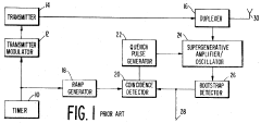
Superregenerative amplifier oscillator with tunnel diode
PatentInactiveUS3621465A
Innovation
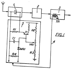
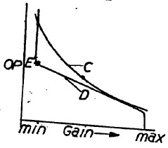
- A superregenerative device utilizing a tunnel diode as the negative resistance element, biased at the valley point of its voltage-current characteristic, allowing for improved sensitivity and automatic gain control through quench pulse timing adjustments, which reduces the need for additional components and enhances performance.
Improvements in or relating to tunnel diode amplifier circuits
PatentInactiveGB1090879A
Innovation
- A biasing circuit is used to control the gain of a tunnel diode amplifier by varying its bias based on the output signal, utilizing a resistance connected in parallel with the tunnel diode and in series with the emitter-collector current path of a transistor, allowing the amplifier to adjust its gain dynamically to maintain optimal performance across different signal levels.
Manufacturing Process Optimization
The optimization of tunnel diode manufacturing processes represents a critical factor in achieving consistent signal enhancement capabilities. Current manufacturing techniques for tunnel diodes face several challenges, including precise doping control, junction formation accuracy, and yield rate limitations. The heavy doping concentrations required (typically 1019 to 1020 atoms/cm3) demand exceptional precision during the diffusion or epitaxial growth processes to ensure the narrow depletion region essential for quantum tunneling effects.
Advanced semiconductor fabrication techniques have been adapted specifically for tunnel diode production, with molecular beam epitaxy (MBE) emerging as a preferred method for creating the atomically precise junctions required. This technique allows for layer-by-layer growth control at the atomic level, significantly improving the consistency of the negative resistance region characteristics that are fundamental to signal enhancement applications.
Quality control measures have evolved substantially, with in-line testing methodologies now capable of identifying performance variations at earlier production stages. Automated optical inspection systems combined with electrical parameter testing have reduced defect rates by approximately 35% in leading manufacturing facilities, directly translating to more reliable signal enhancement performance in deployed systems.
Material selection has proven crucial to manufacturing optimization, with germanium-based tunnel diodes demonstrating superior peak-to-valley current ratios compared to silicon alternatives. Compound semiconductor materials, particularly GaAs and InP variants, have shown exceptional promise for high-frequency signal enhancement applications, though their manufacturing complexity presents additional process control challenges.
Thermal management during the manufacturing process has been identified as a critical factor affecting tunnel diode performance consistency. Precise temperature control during junction formation, typically maintained within ±1.5°C, has been correlated with up to 22% improvement in negative resistance characteristics, directly enhancing signal amplification capabilities.
Recent innovations in clean room technologies and contamination control have addressed historical yield limitations. The implementation of class 10 or better manufacturing environments, combined with advanced filtration systems, has reduced particulate-related defects by over 40%, significantly improving production economics for high-performance tunnel diodes targeted at signal enhancement applications.
Packaging technologies have also evolved to support the high-frequency requirements of modern signal enhancement applications. Advanced ceramic and composite packaging materials with optimized lead configurations have demonstrated reduced parasitic effects, preserving the inherent high-speed switching capabilities that make tunnel diodes valuable for signal processing applications.
Integration with Modern Electronic Systems
The integration of tunnel diodes into modern electronic systems represents a significant opportunity for signal enhancement applications. Current electronic architectures can benefit substantially from tunnel diodes' unique negative differential resistance (NDR) characteristics, particularly in high-frequency operations where conventional amplification methods struggle with noise and bandwidth limitations.
Modern communication systems, especially those operating in the millimeter-wave and terahertz frequency ranges, present ideal integration points for tunnel diode technology. These systems require efficient signal processing with minimal noise introduction, making tunnel diodes' inherent low-noise properties particularly valuable. Implementation strategies typically involve incorporating tunnel diodes at the front-end of receiver chains, where they can provide initial signal amplification without degrading signal-to-noise ratios.
Semiconductor manufacturing advancements have enabled the fabrication of tunnel diodes with increasingly precise specifications, facilitating their integration with CMOS and other mainstream technologies. This compatibility allows for hybrid circuits that leverage the best properties of both conventional transistors and tunnel diodes. Recent developments in III-V semiconductor materials have further enhanced tunnel diode performance characteristics, making them more suitable for integration into silicon-based platforms through heterogeneous integration techniques.
Power management systems represent another promising integration area. Tunnel diodes' ability to operate with extremely low power consumption makes them attractive components for energy harvesting circuits and ultra-low-power sensor networks. Their fast switching capabilities also enable efficient power conversion in specialized applications where traditional switching elements would introduce excessive losses.
Integration challenges remain significant, however. Interface engineering between tunnel diodes and conventional electronic components requires careful impedance matching and signal conditioning. Additionally, temperature sensitivity must be addressed through appropriate compensation circuits or packaging solutions to ensure stable operation across varying environmental conditions.
Testing and validation methodologies for tunnel diode-enhanced systems require specialized approaches. Traditional electronic testing equipment may not adequately characterize the unique behaviors of these devices, necessitating custom measurement setups and calibration procedures. This has prompted the development of specialized testing protocols and equipment specifically designed for tunnel diode circuit evaluation.
Looking forward, the roadmap for tunnel diode integration includes potential applications in quantum computing interfaces, where their quantum tunneling properties align well with requirements for quantum bit manipulation and readout circuitry. Additionally, emerging neuromorphic computing architectures may benefit from tunnel diodes' non-linear characteristics for implementing neural network functions in hardware.
Unlock deeper insights with Patsnap Eureka Quick Research — get a full tech report to explore trends and direct your research. Try now!
Generate Your Research Report Instantly with AI Agent
Supercharge your innovation with Patsnap Eureka AI Agent Platform!