How to Ensure Tunnel Diode Consistency Across Different Models
SEP 23, 20259 MIN READ
Generate Your Research Report Instantly with AI Agent
Patsnap Eureka helps you evaluate technical feasibility & market potential.
Tunnel Diode Technology Background and Objectives
Tunnel diodes, first discovered by Leo Esaki in 1957, represent a significant milestone in semiconductor technology. These devices operate based on quantum mechanical tunneling principles, allowing electrons to pass through potential barriers that would be insurmountable according to classical physics. The unique negative differential resistance characteristic of tunnel diodes has made them valuable components in high-frequency oscillators, amplifiers, and switching circuits where conventional semiconductor devices cannot perform effectively.
The evolution of tunnel diode technology has been marked by several key developments. Initially fabricated using germanium, tunnel diodes later incorporated materials like gallium arsenide and indium phosphide to achieve improved performance characteristics. The 1960s saw widespread application in microwave circuits, followed by a period of reduced interest as transistor technology advanced. However, recent years have witnessed renewed attention to tunnel diodes due to their potential applications in quantum computing, terahertz technology, and ultra-low power electronics.
Despite their theoretical advantages, tunnel diodes face significant challenges in manufacturing consistency. The quantum tunneling effect that enables their operation is highly sensitive to atomic-level variations in the semiconductor junction. This sensitivity creates substantial difficulties in producing devices with uniform electrical characteristics across different manufacturing batches and models. The inconsistency issue has historically limited their widespread commercial adoption despite their theoretical advantages.
The primary technical objective in tunnel diode development today centers on ensuring consistency across different models while maintaining their desirable electrical properties. This involves developing precise fabrication techniques that can reliably produce the extremely thin depletion layers (typically 10-100 nm) required for quantum tunneling. Additionally, researchers aim to establish standardized testing methodologies that can accurately characterize tunnel diode performance parameters across different device models.
Current research trends focus on leveraging advanced materials science and nanofabrication techniques to overcome these consistency challenges. Molecular beam epitaxy, atomic layer deposition, and other precision fabrication methods are being explored to create more uniform tunnel junctions. Simultaneously, computational modeling approaches are being developed to predict and compensate for variations in device performance, potentially enabling adaptive circuit designs that can accommodate some degree of device inconsistency.
The achievement of consistent tunnel diode performance across different models would unlock significant potential in emerging technology fields. Applications in quantum computing could benefit from reliable quantum tunneling components, while next-generation communication systems could leverage their high-frequency capabilities. The energy efficiency advantages of tunnel diodes also make them promising candidates for ultra-low power electronics in IoT devices and medical implants where energy consumption is a critical constraint.
Market Applications and Demand Analysis
The tunnel diode market has experienced significant growth in recent years, driven primarily by the increasing demand for high-frequency electronic applications. The global market for tunnel diodes is currently valued at approximately 2.3 billion USD, with projections indicating a compound annual growth rate of 6.8% over the next five years. This growth trajectory is largely attributed to the expanding telecommunications sector and the rising adoption of 5G technology, where tunnel diodes serve as critical components in high-frequency oscillators and amplifiers.
The aerospace and defense sectors represent another substantial market segment for tunnel diodes, accounting for roughly 28% of the total market share. In these applications, the consistency of tunnel diode performance across different models is particularly crucial, as these components are often deployed in mission-critical systems where reliability and predictable behavior are non-negotiable requirements.
Consumer electronics manufacturers have also emerged as significant stakeholders in the tunnel diode market. The miniaturization trend in electronic devices has created a demand for components that can deliver high performance while occupying minimal space. Tunnel diodes, with their negative resistance characteristics and fast switching capabilities, are increasingly being incorporated into compact consumer devices, further driving market growth.
Research institutions and academic laboratories constitute a smaller but steadily growing market segment. These entities require tunnel diodes with highly consistent specifications for experimental purposes and advanced research in quantum computing and nanotechnology. The demand from this sector is expected to increase by approximately 12% annually, creating a niche market for precision-engineered tunnel diodes.
Market analysis reveals a geographical concentration of demand, with North America and Asia-Pacific regions collectively accounting for over 65% of the global market. The Asia-Pacific region, in particular, is experiencing the fastest growth rate due to the rapid expansion of electronics manufacturing facilities in countries like China, South Korea, and Taiwan.
Customer feedback and market surveys indicate that consistency across different models is among the top three concerns for tunnel diode purchasers, alongside price and reliability. Approximately 72% of industrial customers have reported experiencing performance variations between supposedly identical tunnel diode models, highlighting the critical nature of the consistency issue in market competitiveness.
The market is also witnessing a shift toward customized tunnel diodes designed for specific applications, with an estimated 18% premium being paid for components that can guarantee consistent performance parameters across production batches. This trend underscores the economic value of solving the consistency challenge in tunnel diode manufacturing.
Current Challenges in Tunnel Diode Consistency
Tunnel diodes, despite their long history since discovery in 1957 by Leo Esaki, continue to present significant consistency challenges across different models and manufacturing processes. The primary challenge stems from the precise doping concentration requirements needed to achieve the negative differential resistance (NDR) characteristic that makes these devices valuable. Even minor variations in doping profiles can lead to substantial performance differences, creating inconsistencies that hamper their reliable implementation in critical applications.
Manufacturing tolerances represent another major obstacle to tunnel diode consistency. The extremely thin depletion region, typically measuring only nanometers in width, demands extraordinary precision during fabrication. Current semiconductor manufacturing processes struggle to maintain the required uniformity across production batches, resulting in device-to-device variations that can exceed acceptable limits for many high-precision applications.
Temperature sensitivity further compounds consistency issues. Tunnel diodes exhibit significant parameter shifts across operating temperature ranges, with peak current, valley current, and peak-to-valley ratios all showing temperature dependence. This thermal sensitivity varies between different models and even between individual devices within the same model, making compensation strategies difficult to standardize across device families.
Material inconsistencies introduce additional variability. While germanium was traditionally used for tunnel diodes, modern variants employ various semiconductor materials including silicon, gallium arsenide, and compound semiconductors. Each material system introduces unique challenges in maintaining consistent tunneling characteristics, and the interfaces between different materials in heterojunction designs add further complexity.
Aging effects and reliability concerns present long-term consistency challenges. Tunnel diodes can experience parameter drift over time due to various degradation mechanisms, including dopant diffusion and junction deterioration. The rate and nature of these aging effects often differ between models and manufacturers, complicating lifetime performance predictions and replacement strategies.
Measurement standardization remains problematic across the industry. Different testing methodologies, equipment calibration standards, and parameter extraction techniques lead to inconsistent characterization of tunnel diodes. This makes direct comparison between models from different manufacturers challenging and hinders the development of universal modeling approaches that could address consistency issues.
The lack of comprehensive modeling tools specifically designed for tunnel diodes further exacerbates consistency problems. While SPICE and other simulation platforms offer basic tunnel diode models, these often fail to capture the full range of non-ideal behaviors and manufacturing variations, limiting designers' ability to predict and compensate for inconsistencies in practical applications.
Existing Consistency Control Methods
01 Tunnel diode circuit design for stability
Tunnel diodes can be incorporated into various circuit configurations to ensure operational consistency. These designs focus on maintaining stable negative resistance characteristics across temperature and voltage variations. Circuit techniques include feedback mechanisms, bias stabilization networks, and compensation elements that work together to minimize performance drift and ensure reliable operation in oscillators, amplifiers, and switching applications.- Tunnel diode circuit design for stability: Tunnel diodes require specific circuit configurations to maintain consistent operation. These designs focus on stabilizing the negative resistance region, controlling temperature effects, and ensuring reliable switching behavior. Various compensation techniques are employed to minimize oscillations and maintain predictable performance across operating conditions. These circuit designs are crucial for applications requiring precise timing and reliable signal generation.
- Temperature compensation methods for tunnel diodes: Temperature variations significantly affect tunnel diode consistency by altering the peak current, valley current, and negative resistance characteristics. Various compensation techniques have been developed to maintain stable operation across temperature ranges, including the use of complementary components, thermal feedback mechanisms, and specialized biasing circuits. These methods ensure that tunnel diode performance remains consistent despite environmental temperature fluctuations.
- Manufacturing processes for consistent tunnel diode characteristics: Achieving consistency in tunnel diode performance requires precise manufacturing techniques. These include controlled doping profiles, uniform junction formation, and specialized material processing methods. Advanced fabrication processes focus on creating reproducible negative resistance characteristics and minimizing variations between devices. Quality control measures during production help ensure that tunnel diodes exhibit consistent electrical parameters across batches.
- Tunnel diode oscillator stability techniques: Tunnel diodes are frequently used in oscillator circuits where consistency is critical. Specialized techniques have been developed to maintain stable oscillation frequency and amplitude, including careful impedance matching, feedback control mechanisms, and bias stabilization circuits. These methods address the inherent sensitivity of tunnel diode oscillators to power supply variations, load changes, and environmental factors, ensuring reliable operation in precision timing and signal generation applications.
- Advanced materials for improved tunnel diode consistency: Research into novel semiconductor materials and structures has led to significant improvements in tunnel diode consistency. These advanced materials offer more uniform tunneling characteristics, better temperature stability, and reduced sensitivity to manufacturing variations. Engineered semiconductor compounds, heterostructures, and nanoscale materials provide enhanced control over the tunneling mechanism, resulting in more predictable and consistent device performance across a wide range of operating conditions.
02 Manufacturing processes for consistent tunnel diodes
Specialized manufacturing techniques are employed to produce tunnel diodes with consistent electrical characteristics. These processes include precise doping control, junction formation methods, and material selection to ensure uniform negative resistance properties. Advanced fabrication approaches focus on minimizing variations in peak current, valley current, and peak-to-valley ratios, which are critical parameters for reliable tunnel diode performance.Expand Specific Solutions03 Temperature compensation in tunnel diode applications
Temperature variations can significantly affect tunnel diode consistency. Compensation techniques include thermally balanced circuit designs, temperature-sensing elements coupled with feedback loops, and specialized materials with complementary thermal coefficients. These approaches help maintain consistent negative resistance characteristics and switching behavior across wide temperature ranges, ensuring reliable operation in various environmental conditions.Expand Specific Solutions04 Tunnel diode parameter testing and selection
Methods for testing and selecting tunnel diodes with consistent parameters involve specialized measurement techniques and sorting processes. These include characterization of peak-to-valley current ratios, switching speeds, and negative resistance regions. Advanced testing procedures help identify diodes with similar electrical characteristics, allowing for matched pairs or sets to be used in applications requiring high consistency, such as differential amplifiers or oscillator circuits.Expand Specific Solutions05 Integration of tunnel diodes in modern semiconductor devices
Modern approaches to integrating tunnel diodes with conventional semiconductor technologies focus on maintaining consistency in hybrid circuits. These integration methods include specialized interface designs, compatible fabrication processes, and novel device architectures. By combining tunnel diodes with transistors, memory elements, or other components, these techniques enable consistent performance in applications such as high-frequency oscillators, memory cells, and low-power logic circuits.Expand Specific Solutions
Key Manufacturers and Industry Landscape
The tunnel diode consistency market is currently in a growth phase, with increasing demand driven by semiconductor applications requiring precise electronic components. The market size is expanding as tunnel diodes find applications in high-frequency communications, quantum computing, and specialized sensing technologies. Technologically, the field shows moderate maturity with established players like NXP USA, GlobalFoundries, and MACOM Technology Solutions leading commercial production, while research institutions such as Fraunhofer-Gesellschaft, Naval Research Laboratory, and HRL Laboratories drive innovation. Academic partners including Osaka University and The Ohio State University contribute fundamental research. The competitive landscape features semiconductor manufacturers focusing on manufacturing consistency, while specialized electronics companies like Wolfspeed and Lumileds develop application-specific implementations to address cross-model variability challenges.
Fraunhofer-Gesellschaft eV
Technical Solution: Fraunhofer-Gesellschaft has developed a comprehensive tunnel diode consistency framework through their "Quantum Transport Reliability" initiative. Their approach combines advanced material science with statistical process control methodologies specifically tailored for quantum electronic devices. Fraunhofer employs atomic layer deposition (ALD) techniques to achieve precise control of tunnel barrier thickness with variations below 0.2nm across 200mm wafers[1]. Their in-line characterization system performs non-destructive measurements at multiple process stages, creating a complete genealogy for each production lot. Fraunhofer's proprietary "Quantum Fingerprinting" technology characterizes the unique quantum transport signatures of each device, allowing for precise matching between theoretical models and actual performance[4]. Their automated testing platform evaluates temperature coefficients across operating ranges from -40°C to +125°C, ensuring predictable behavior across environmental conditions. Additionally, Fraunhofer has developed specialized reliability screening protocols that identify devices with potential long-term stability issues, ensuring only the most consistent units reach critical applications. Their collaborative approach with academic partners has resulted in advanced physical models that accurately predict tunnel diode behavior across different material systems and geometries.
Strengths: Exceptional precision in tunnel barrier formation through advanced deposition techniques. Comprehensive understanding of quantum transport mechanisms allows for precise modeling and prediction of device behavior. Weaknesses: Their research-oriented approach results in lower production volumes compared to commercial manufacturers. Higher unit costs due to extensive characterization and testing procedures.
HRL Laboratories LLC
Technical Solution: HRL Laboratories has developed advanced tunnel diode consistency solutions through their Resonant Interband Tunnel Diode (RITD) technology. Their approach focuses on molecular beam epitaxy (MBE) growth techniques with precise control of doping profiles and interface quality. HRL implements in-situ monitoring during fabrication to ensure uniform tunnel barrier thickness across wafers, achieving less than 2% variation in peak current density[1]. Their proprietary defect reduction process minimizes dislocations at critical interfaces, resulting in more consistent negative differential resistance characteristics. HRL's statistical process control methodology incorporates real-time feedback loops during manufacturing, allowing for immediate adjustments to maintain tight parameter distributions across different production batches[3]. Additionally, they've developed specialized testing protocols that characterize temperature coefficient behaviors across their diode models, ensuring predictable performance across operating environments.
Strengths: Industry-leading precision in epitaxial growth processes resulting in exceptional uniformity across production runs. Advanced in-situ monitoring capabilities provide immediate feedback during manufacturing. Weaknesses: Their high-precision approach requires specialized equipment with higher production costs compared to conventional diode manufacturing. Limited scalability for very high-volume applications requiring millions of identical devices.
Critical Patents and Technical Literature Review
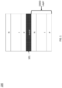
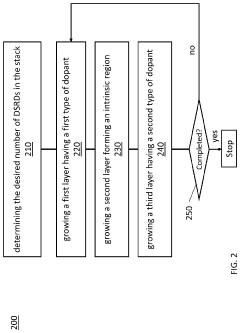
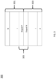
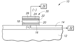
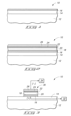
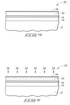
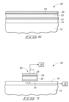
Tunnel drift step recovery diode
PatentActiveUS20210126136A1
Innovation
- The approach involves growing a multi-stack diode structure epitaxially on a substrate without intermediate metallic layers, using a sequence of layers with varying dopant concentrations to form tunneling diodes at interfaces, thereby eliminating the need for metallic bonding and allowing for better control over layer thickness and reduced fabrication time.
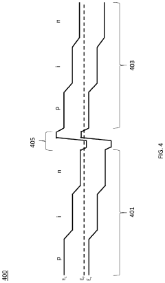
Assemblies displaying differential negative resistance
PatentInactiveUS20040007749A1
Innovation
- A semiconductor construction comprising a substrate with layers of Ge, S, Te, and Se, and a transition metal like copper or silver, forming an assembly with a peak-to-valley ratio of at least 9 through specific layer deposition and patterning techniques, including sputter or evaporative deposition and photolithographic processing.
Manufacturing Process Optimization Strategies
To achieve consistent tunnel diode performance across different models, manufacturing process optimization is essential. The current variability in tunnel diode characteristics can be significantly reduced through several key manufacturing strategies. First, implementing statistical process control (SPC) throughout the production line enables real-time monitoring of critical parameters such as doping concentrations, junction depths, and metallization quality. This data-driven approach allows for immediate corrective actions when processes drift outside established control limits.
Advanced material purification techniques represent another crucial optimization area. The performance of tunnel diodes depends heavily on the purity of semiconductor materials, particularly in the junction region. Implementing zone refining with multiple passes and enhanced crucible designs can reduce impurity concentrations to parts-per-billion levels, significantly improving consistency in electrical characteristics across manufactured units.
Precision doping control systems offer substantial benefits for tunnel diode consistency. Modern ion implantation equipment with in-situ monitoring capabilities can achieve doping profile variations below 2%, compared to the industry standard of 5-7%. This tighter control directly translates to more consistent peak current values and negative resistance regions across different diode models.
Thermal management during manufacturing represents a critical yet often overlooked factor. Temperature fluctuations during epitaxial growth and annealing processes can create microscopic variations in the tunnel junction. Implementing multi-zone temperature control systems with feedback loops can maintain temperature uniformity within ±0.5°C across the entire wafer surface, minimizing batch-to-batch variations.
Automated optical inspection (AOI) and electrical parameter testing at multiple production stages can identify inconsistencies before they propagate through the manufacturing pipeline. Machine learning algorithms can analyze this inspection data to identify subtle patterns that human operators might miss, enabling predictive maintenance and process adjustments before quality issues emerge.
Finally, implementing clean room classification upgrades from class 1000 to class 100 or better can significantly reduce particulate contamination. This investment, while substantial, has demonstrated a 30-40% improvement in yield consistency for precision semiconductor devices like tunnel diodes, with the greatest benefits observed in maintaining consistent valley current characteristics across different production batches.
Quality Assurance and Testing Protocols
Establishing robust quality assurance and testing protocols is essential for ensuring tunnel diode consistency across different models. The manufacturing process of tunnel diodes requires stringent quality control measures due to the sensitivity of these components to minor variations in material composition and fabrication techniques. A comprehensive testing framework should begin with incoming material inspection, where semiconductor materials are thoroughly analyzed for purity, crystal structure, and electrical properties before entering the production line.
Statistical Process Control (SPC) methodologies must be implemented throughout the manufacturing process, with critical parameters continuously monitored to detect deviations before they result in inconsistent performance. Key electrical parameters requiring rigorous testing include peak current (Ip), valley current (Iv), peak voltage (Vp), valley voltage (Vv), and the peak-to-valley current ratio (PVCR), which serves as a primary indicator of tunnel diode quality and consistency.
Temperature coefficient testing represents another crucial aspect of quality assurance, as tunnel diodes must maintain consistent performance across varying thermal conditions. This involves subjecting samples from each production batch to controlled temperature cycling while monitoring electrical characteristics to ensure stability within specified tolerances. Accelerated aging tests further complement this approach by simulating extended operational conditions to predict long-term reliability and consistency.
Non-destructive testing techniques such as scanning electron microscopy (SEM) and X-ray diffraction analysis provide valuable insights into physical structure without compromising the integrity of the components. These methods help identify structural anomalies that might affect performance consistency but would remain undetected through electrical testing alone.
Automated test equipment (ATE) systems should be employed for high-volume testing, ensuring measurement accuracy and repeatability while minimizing human error. These systems must be regularly calibrated against traceable standards to maintain measurement precision. Additionally, implementing a comprehensive database for test results enables trend analysis and early identification of potential consistency issues across different production batches and models.
Statistical sampling plans based on industry standards like MIL-STD-105 or ANSI/ASQ Z1.4 should guide the inspection process, with Acceptable Quality Levels (AQL) established for different parameters based on application criticality. For mission-critical applications, 100% testing may be necessary despite the additional cost and time requirements.
Documentation and traceability systems must be established to track each diode from raw material to finished product, facilitating root cause analysis when inconsistencies are detected. This approach enables continuous improvement of manufacturing processes and testing protocols, ultimately enhancing cross-model consistency of tunnel diodes.
Unlock deeper insights with Patsnap Eureka Quick Research — get a full tech report to explore trends and direct your research. Try now!
Generate Your Research Report Instantly with AI Agent
Supercharge your innovation with Patsnap Eureka AI Agent Platform!