

How to Test Tunnel Diode Resistance Changes
SEP 23, 20259 MIN READ
Generate Your Research Report Instantly with AI Agent
Patsnap Eureka helps you evaluate technical feasibility & market potential.
Tunnel Diode Testing Background and Objectives
Tunnel diodes, first discovered by Leo Esaki in 1957, represent a significant breakthrough in semiconductor technology. These specialized diodes exhibit a unique negative resistance region in their current-voltage characteristics, making them valuable components in high-frequency oscillators, amplifiers, and switching circuits. The evolution of tunnel diode technology has progressed from early germanium-based devices to more advanced gallium arsenide and indium phosphide implementations, each offering improved performance characteristics.
The primary objective of tunnel diode resistance testing is to accurately characterize the negative differential resistance (NDR) region, which is the defining feature that distinguishes tunnel diodes from conventional semiconductor devices. This region, where current decreases as voltage increases, enables unique circuit applications that cannot be achieved with standard components. Precise measurement of this resistance change is critical for quality control in manufacturing, performance verification, and reliability assessment.
Historical testing methodologies for tunnel diodes have evolved significantly since their inception. Early approaches relied on basic current-voltage sweeps, which often failed to capture the full dynamics of the NDR region due to measurement instabilities. Modern testing aims to overcome these limitations through advanced techniques that can accurately characterize the complete I-V curve, including the critical peak and valley points that define the boundaries of the NDR region.
The technical goals for tunnel diode resistance testing encompass several dimensions. First, achieving high measurement accuracy is essential, particularly in the NDR region where small variations can significantly impact device performance. Second, testing methods must be capable of operating at the high frequencies where tunnel diodes typically function, often extending into the microwave range. Third, testing solutions should be adaptable to various tunnel diode materials and configurations to accommodate ongoing technological advancements.
Current industry trends are pushing toward non-destructive testing methods that can be integrated into automated production environments. This shift is driven by the increasing application of tunnel diodes in specialized fields such as quantum computing, terahertz technology, and ultra-high-speed communications, where precise performance characteristics are critical.
The development of standardized testing protocols represents another important objective, as it would enable consistent comparison of devices across manufacturers and applications. Such standardization would facilitate broader adoption of tunnel diode technology in emerging fields and support continued innovation in device design and fabrication techniques.
Market Applications for Tunnel Diode Resistance Measurement
Tunnel diode resistance measurement technology has found significant applications across multiple industries due to its unique capabilities in detecting subtle resistance changes. In the semiconductor industry, these measurements are crucial for quality control during manufacturing processes, allowing for precise characterization of tunnel diode parameters and ensuring consistency in production. The technology enables manufacturers to identify defective components early in the production cycle, significantly reducing waste and improving yield rates.
The telecommunications sector represents another substantial market for tunnel diode resistance measurement. As 5G networks continue to expand globally, the demand for high-frequency components with precise electrical characteristics has increased dramatically. Tunnel diodes, with their negative resistance properties and fast switching capabilities, serve critical functions in high-frequency communication systems. The ability to accurately measure resistance changes enables telecom equipment manufacturers to optimize performance and reliability of their systems.
Aerospace and defense applications constitute a premium market segment for this technology. In satellite communications, radar systems, and military electronics, tunnel diodes operate in extreme environments where performance stability is paramount. Resistance measurement technologies allow for comprehensive testing under simulated environmental conditions, ensuring components will function reliably in space, at high altitudes, or in battlefield conditions.
The medical device industry has emerged as a growing application area, particularly in diagnostic equipment requiring high-frequency oscillators and sensitive detection circuits. Tunnel diodes provide advantages in terms of low noise and high sensitivity, making them valuable in medical imaging and monitoring devices. Accurate resistance measurement ensures these critical components meet stringent healthcare industry standards.
Research institutions and academic laboratories represent a specialized but important market. Advanced physics research, quantum computing development, and materials science investigations all utilize tunnel diodes for their unique electrical properties. Precise resistance measurement tools are essential for experimental validation and theoretical model development in these cutting-edge fields.
The emerging quantum computing sector presents perhaps the most promising future growth market. Tunnel diodes' quantum tunneling properties make them potentially valuable components in quantum circuit development. As this field advances, the demand for increasingly precise measurement technologies will grow proportionally, creating opportunities for specialized testing equipment manufacturers.
Industrial automation and control systems also benefit from tunnel diode resistance measurement technology, particularly in environments with electromagnetic interference where tunnel diodes' inherent noise resistance provides advantages over conventional semiconductor devices. The ability to verify proper functioning through resistance testing contributes to system reliability in critical industrial applications.
Current Testing Challenges and Limitations
Testing tunnel diode resistance changes presents several significant challenges that limit the accuracy, reliability, and efficiency of current measurement methods. The non-linear characteristics of tunnel diodes create fundamental difficulties in resistance measurement, as the negative resistance region exhibits unique behaviors that conventional testing equipment struggles to capture accurately. This non-linearity means that standard resistance measurement techniques, which assume ohmic behavior, produce inconsistent and often misleading results.
Temperature sensitivity poses another major challenge, as tunnel diode resistance parameters can vary significantly with even minor temperature fluctuations. Current testing setups often lack adequate temperature control mechanisms, leading to measurement drift and poor repeatability. This environmental dependency makes it difficult to establish standardized testing protocols that can be reliably implemented across different laboratory conditions.
The high-frequency response characteristics of tunnel diodes further complicate testing procedures. Most conventional resistance measurement equipment operates at relatively low frequencies, while tunnel diodes exhibit their most interesting behaviors at higher frequencies. This frequency mismatch means that static resistance measurements fail to capture the dynamic performance characteristics that are often most relevant to practical applications.
Measurement resolution limitations represent another significant barrier. The negative resistance region of tunnel diodes occurs within a very narrow voltage range, typically just tens of millivolts. Standard multimeters and testing equipment often lack the precision required to accurately characterize these subtle resistance transitions, resulting in missed or misinterpreted resistance change events.
Contact resistance and parasitic effects introduce additional measurement uncertainties. The extremely small size of modern tunnel diodes means that probe contact resistance can be comparable to or even exceed the device resistance being measured. These parasitic elements create measurement artifacts that can mask the true resistance behavior of the device under test.
Standardization issues further complicate the testing landscape. Unlike many other electronic components, tunnel diodes lack universally accepted testing methodologies and specifications. This absence of standardization makes it difficult to compare results across different research groups or manufacturing facilities, hampering collaborative development efforts and quality control processes.
Finally, current testing approaches typically require specialized equipment that is both expensive and requires significant expertise to operate correctly. This high barrier to entry limits widespread adoption of tunnel diode technology and restricts testing capabilities to well-funded research institutions and large manufacturing facilities, slowing innovation and commercialization efforts in this promising technology domain.
Existing Resistance Testing Solutions and Protocols
01 Negative resistance characteristics of tunnel diodes
Tunnel diodes exhibit a unique negative resistance region in their current-voltage characteristics. This property occurs when an increase in voltage leads to a decrease in current, which is contrary to conventional resistive behavior. This negative resistance characteristic makes tunnel diodes valuable for various electronic applications including oscillators, amplifiers, and switching circuits. The negative resistance region is a result of quantum tunneling effects that occur in heavily doped semiconductor junctions.- Negative resistance characteristics of tunnel diodes: Tunnel diodes exhibit a unique negative resistance region in their current-voltage characteristics, where an increase in voltage results in a decrease in current. This property makes them valuable in various electronic applications such as oscillators, amplifiers, and switching circuits. The negative resistance behavior occurs due to quantum tunneling effects and is a fundamental characteristic that distinguishes tunnel diodes from conventional semiconductor devices.
- Tunnel diode resistance in circuit applications: The resistance properties of tunnel diodes are exploited in various circuit applications. When properly biased in the negative resistance region, tunnel diodes can be used in oscillator circuits, pulse generators, and high-frequency applications. The resistance characteristics can be controlled through proper biasing techniques, allowing for optimization in specific circuit configurations. These applications leverage the unique current-voltage relationship to achieve performance not possible with conventional components.
- Temperature effects on tunnel diode resistance: Temperature significantly affects the resistance characteristics of tunnel diodes. As temperature increases, the negative resistance region may shift or become less pronounced due to changes in carrier mobility and tunneling probability. Circuit designs incorporating tunnel diodes must account for these temperature dependencies to maintain stable operation across varying environmental conditions. Compensation techniques and temperature-stabilized biasing networks are often employed to mitigate these effects.
- Manufacturing techniques affecting tunnel diode resistance: The resistance characteristics of tunnel diodes are heavily influenced by manufacturing processes and material selection. Doping concentration, junction formation techniques, and semiconductor material quality directly impact the peak-to-valley current ratio and the width of the negative resistance region. Advanced fabrication methods, including precise epitaxial growth and controlled doping profiles, have been developed to optimize tunnel diode resistance properties for specific applications.
- Measurement and characterization of tunnel diode resistance: Accurate measurement and characterization of tunnel diode resistance parameters are essential for device modeling and circuit design. Specialized test equipment and methodologies have been developed to precisely determine the negative resistance characteristics, peak current points, and valley voltage values. These measurements enable engineers to select appropriate tunnel diodes for specific applications and to develop accurate simulation models that predict circuit behavior under various operating conditions.
02 Tunnel diode resistance in circuit applications
Tunnel diodes are utilized in various circuit applications due to their resistance properties. Their small-signal resistance characteristics make them suitable for high-frequency operations, including microwave circuits and oscillators. The resistance of tunnel diodes can be controlled and manipulated in circuits to achieve specific functionalities such as amplification, switching, and signal generation. Circuit designers leverage both the positive and negative resistance regions of tunnel diodes to create efficient electronic systems.Expand Specific Solutions03 Temperature effects on tunnel diode resistance
The resistance characteristics of tunnel diodes are significantly influenced by temperature variations. As temperature changes, the tunneling probability and carrier concentration in the semiconductor material are affected, which alters the resistance profile of the device. Understanding and compensating for these temperature dependencies is crucial for designing stable circuits using tunnel diodes. Some applications specifically utilize the temperature sensitivity of tunnel diode resistance for sensing or compensation purposes.Expand Specific Solutions04 Manufacturing techniques affecting tunnel diode resistance
Various manufacturing and fabrication techniques significantly impact the resistance characteristics of tunnel diodes. The doping concentration, junction area, and material selection directly influence the peak-to-valley current ratio and the negative resistance region. Advanced manufacturing processes can optimize these parameters to achieve desired resistance profiles for specific applications. Innovations in semiconductor processing have enabled the production of tunnel diodes with improved resistance characteristics and performance stability.Expand Specific Solutions05 Modern applications utilizing tunnel diode resistance
Contemporary applications leverage the unique resistance properties of tunnel diodes in novel ways. These include high-speed digital circuits, quantum computing components, and energy-efficient electronic systems. The distinctive negative resistance characteristic enables the development of compact oscillators and memory cells with reduced power consumption. Recent research has explored integrating tunnel diodes with other semiconductor devices to create hybrid systems that benefit from their special resistance properties while overcoming traditional limitations.Expand Specific Solutions
Key Industry Players in Tunnel Diode Technology
The tunnel diode resistance testing technology landscape is currently in a growth phase, with increasing market demand driven by semiconductor applications. The market is expected to reach significant scale as tunnel diodes find applications in high-frequency oscillators, amplifiers, and switching circuits. Technologically, the field shows moderate maturity with established players like Samsung Electronics, Fujitsu, and TDK Corp leading commercial applications, while research institutions such as Southwest Jiaotong University and CNRS advance fundamental testing methodologies. Taiwan Semiconductor Manufacturing and Infineon Technologies are developing integrated testing solutions, while specialized equipment manufacturers like Canon Anelva and MACOM focus on precision measurement tools for resistance characterization in tunnel diode applications.
Fujitsu Ltd.
Technical Solution: Fujitsu has developed advanced tunnel diode resistance testing methodologies using high-precision impedance analyzers that operate across multiple frequency ranges (from DC to GHz). Their approach incorporates automated measurement systems with temperature control chambers to characterize tunnel diode resistance changes under varying environmental conditions. The company utilizes proprietary signal processing algorithms to filter noise and extract accurate resistance parameters from raw measurement data. Fujitsu's testing platform integrates with their broader semiconductor characterization systems, allowing for comprehensive analysis of tunnel diode performance including peak-to-valley current ratio measurements, switching speed assessments, and resistance stability over time. Their methodology includes specialized probe stations with four-point measurement capabilities to eliminate contact resistance effects that can obscure true tunnel diode behavior.
Strengths: Superior noise rejection capabilities allowing for measurements in industrial environments; integrated data analysis software provides comprehensive performance metrics beyond simple resistance measurements. Weaknesses: System complexity requires specialized training; higher implementation costs compared to simpler testing approaches.
TDK Corp.
Technical Solution: TDK has engineered a specialized tunnel diode resistance measurement system that employs pulsed current techniques to prevent device self-heating during testing. Their approach utilizes custom-designed low-noise amplifiers and precision current sources capable of sub-nanosecond pulse generation to capture the negative resistance region characteristics accurately. TDK's testing methodology incorporates temperature-compensated reference circuits and calibration standards specifically developed for tunnel diode applications. The company's testing platform features automated I-V curve tracing with high sampling rates (>100 MSa/s) to capture the complete resistance profile including the negative differential resistance region. Their system includes specialized fixtures with controlled impedance paths to minimize measurement artifacts and reflection issues that can distort resistance measurements in high-frequency applications.
Strengths: Exceptional temporal resolution allows capture of transient resistance changes; specialized fixtures minimize parasitic effects. Weaknesses: Limited throughput for high-volume production testing; requires frequent calibration to maintain measurement accuracy.
Critical Testing Technologies and Patents
Method and apparatus for testing tunnel magnetoresistive effect element, manufacturing method of tunnel magnetoresistive effect element and tunnel magnetoresistive effect element
PatentInactiveUS20060216837A1
Innovation
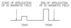
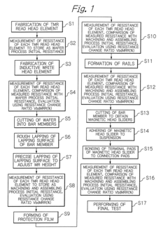
- A method involving the application of multiple voltages with different values to TMR elements to measure resistance changes, calculating the ratio of change in resistance (VbdMRR%), and evaluating the elements based on this ratio, allowing for quick and easy confirmation of reliability without damaging the elements.
Improvements in or relating to tunnel diode circuits
PatentInactiveGB894028A
Innovation
- A tunnel diode is connected in parallel with a variable resistance element, where the gain is controlled by a signal derived from the amplifier's output, using a pilot signal to adjust the resistance and maintain stable gain through a feedback mechanism.
Measurement Accuracy and Calibration Standards
Achieving high measurement accuracy in tunnel diode resistance testing requires adherence to rigorous calibration standards and methodologies. The inherent non-linear characteristics of tunnel diodes, coupled with their sensitivity to temperature variations and electromagnetic interference, necessitate precision measurement techniques. Industry standards such as IEEE 1241 and IEC 60747-7 provide frameworks for semiconductor device testing that can be adapted specifically for tunnel diode resistance measurements.
Calibration of measurement equipment represents a critical prerequisite for reliable resistance change detection. Test equipment should undergo regular calibration against traceable standards, with verification performed before each significant measurement session. The calibration process must account for the unique voltage-current characteristics of tunnel diodes, particularly in the negative resistance region where conventional calibration methods may prove inadequate.
Measurement accuracy is significantly influenced by environmental factors. Temperature stability within ±0.5°C is essential, as tunnel diodes exhibit temperature coefficients that can mask actual resistance changes. Similarly, electromagnetic shielding must be implemented to prevent external signals from corrupting measurement data, especially when working with high-frequency testing protocols.
Statistical validation techniques enhance measurement reliability. Implementing multiple measurement cycles with statistical analysis helps identify outliers and establish confidence intervals. Recommended practices include performing at least five measurement cycles per test condition and calculating standard deviation to quantify measurement uncertainty.
Resolution limitations of testing equipment directly impact measurement accuracy. For detecting subtle resistance changes in tunnel diodes, equipment with resolution capabilities of at least 0.1% of the expected resistance value is necessary. High-precision source-measure units (SMUs) with four-wire (Kelvin) connection configurations minimize lead resistance effects and improve measurement fidelity.
Calibration standards specific to tunnel diode testing remain an evolving field. Current best practices involve using precision resistor networks that simulate the diode's behavior across its operating range. These calibration standards should be certified by national metrology institutes and include characterization data across the temperature range of intended operation.
Traceability to national and international standards ensures measurement consistency across different laboratories and testing facilities. Documentation of calibration procedures, including uncertainty calculations following the guidelines in ISO/IEC Guide 98-3 (GUM), provides essential quality assurance for tunnel diode resistance measurements in both research and production environments.
Environmental Factors Affecting Test Reliability
The reliability of tunnel diode resistance measurements is significantly influenced by various environmental factors that must be carefully controlled during testing procedures. Temperature fluctuations represent one of the most critical variables, as tunnel diodes exhibit pronounced temperature sensitivity that can alter their resistance characteristics. Even minor temperature variations of 1-2°C can lead to measurable changes in the negative resistance region, potentially masking the actual resistance changes being studied. Testing environments should maintain temperature stability within ±0.5°C for high-precision measurements, with continuous monitoring throughout the testing process.
Humidity levels similarly impact test reliability by affecting the surface properties of semiconductor materials. Excessive moisture can create micro-condensation on diode surfaces, introducing parasitic conductance paths that distort resistance readings. Optimal testing conditions typically require relative humidity control between 30-50%, with particular attention needed when testing uncapsulated devices or those with exposed junction areas.
Electromagnetic interference (EMI) constitutes another significant environmental challenge, as tunnel diodes operate with small signal levels that are susceptible to external electrical noise. Nearby equipment, power lines, or wireless communications can introduce measurement artifacts that appear as resistance fluctuations. Proper EMI shielding, including Faraday cages for sensitive measurements and appropriate grounding techniques, becomes essential for obtaining consistent results.
Mechanical vibration presents an often-overlooked environmental factor that can affect measurement stability. Vibrations may induce mechanical stress on the diode structure or create intermittent connection issues in the test fixture. This is particularly relevant when measuring resistance changes at high frequencies or when using probe-based test setups. Anti-vibration tables and isolation platforms can significantly improve measurement consistency in environments prone to mechanical disturbances.
Atmospheric pressure variations, while subtle in most laboratory settings, can influence measurements when testing hermetically sealed devices or when operating near the diode's thermal limits. Barometric pressure changes may alter the thermal conductivity of the surrounding medium, affecting heat dissipation characteristics and consequently the diode's resistance profile.
Light exposure represents a final environmental consideration, as photons striking semiconductor materials can generate electron-hole pairs that temporarily alter device characteristics. This photoelectric effect is particularly relevant for tunnel diodes with exposed semiconductor regions. Testing should occur under controlled lighting conditions, with light-sensitive devices requiring opaque enclosures to ensure measurement consistency.
Unlock deeper insights with Patsnap Eureka Quick Research — get a full tech report to explore trends and direct your research. Try now!
Generate Your Research Report Instantly with AI Agent
Supercharge your innovation with Patsnap Eureka AI Agent Platform!