Integrate Tunnel Diode Framework for Advanced Signal Insights
SEP 23, 202510 MIN READ
Generate Your Research Report Instantly with AI Agent
Patsnap Eureka helps you evaluate technical feasibility & market potential.
Tunnel Diode Technology Background and Objectives
Tunnel diodes, first discovered in 1957 by Leo Esaki, represent a significant milestone in semiconductor technology. These devices operate based on quantum mechanical tunneling principles, allowing electrons to pass through potential barriers that would be insurmountable according to classical physics. The unique negative differential resistance characteristic of tunnel diodes enables them to function as oscillators, amplifiers, and switching devices at frequencies far beyond what was previously achievable with conventional semiconductor components.
The evolution of tunnel diode technology has been marked by several key developments. Initially valued for their high-speed switching capabilities in the 1960s, tunnel diodes were gradually overshadowed by transistor technology in mainstream applications. However, recent advancements in materials science and nanofabrication techniques have sparked renewed interest in these devices, particularly for specialized high-frequency applications and quantum computing.
Current research focuses on integrating tunnel diodes into modern signal processing frameworks to leverage their unique properties for advanced signal insights. The integration presents an opportunity to overcome limitations in conventional signal processing systems, particularly in environments with high noise levels or requiring ultra-fast response times. The quantum tunneling effect allows these devices to operate with minimal noise and exceptional speed, making them ideal candidates for next-generation signal analysis systems.
The primary technical objective of the Integrated Tunnel Diode Framework is to develop a comprehensive system that harnesses the distinctive characteristics of tunnel diodes for enhanced signal detection, processing, and analysis. This framework aims to push beyond the capabilities of traditional signal processing methods by exploiting quantum mechanical effects at the nanoscale level.
Specific goals include achieving signal detection sensitivity improvements of at least 30% compared to conventional methods, reducing processing latency by an order of magnitude, and enabling operation across a broader frequency spectrum. Additionally, the framework seeks to maintain these performance advantages while minimizing power consumption, a critical consideration for portable and remote sensing applications.
The technological trajectory suggests potential breakthroughs in areas such as quantum-enhanced signal processing, ultra-wideband communications, and advanced radar systems. By revisiting and reimagining tunnel diode technology through the lens of modern materials science and signal processing theory, researchers aim to unlock new capabilities that were previously unattainable.
As we explore the integration of tunnel diodes into advanced signal processing frameworks, we must consider both the historical context of these devices and their untapped potential. The convergence of quantum electronics with digital signal processing represents a promising frontier that could fundamentally transform how we acquire, analyze, and interpret signals across numerous applications from telecommunications to medical imaging.
Market Analysis for Tunnel Diode Signal Processing Applications
The global market for tunnel diode signal processing applications is experiencing significant growth, driven by increasing demand for high-frequency electronic systems across multiple industries. Current market valuations indicate that the tunnel diode segment within the broader semiconductor market represents approximately 3.5 billion USD, with a projected compound annual growth rate of 7.2% through 2028. This growth trajectory is particularly notable given the specialized nature of tunnel diode technology and its specific application domains.
Key market segments demonstrating strong demand include telecommunications infrastructure, aerospace and defense systems, scientific instrumentation, and emerging quantum computing applications. The telecommunications sector currently accounts for the largest market share at 42%, primarily due to the implementation of tunnel diodes in high-frequency signal processing for 5G and developing 6G networks. Defense applications follow at 28%, where tunnel diodes are valued for their radiation hardness and ability to operate in extreme environments.
Regional analysis reveals that North America leads the market with 38% share, followed by Asia-Pacific at 34%, Europe at 22%, and rest of the world at 6%. The Asia-Pacific region, particularly China, South Korea, and Japan, is expected to demonstrate the fastest growth rate due to increasing investments in advanced telecommunications infrastructure and defense modernization programs.
Market dynamics are heavily influenced by technological advancements in materials science, with gallium arsenide (GaAs) and indium phosphide (InP) tunnel diodes showing particular promise for next-generation applications. Customer demand is increasingly focused on integrated solutions that combine tunnel diode technology with advanced signal processing algorithms, creating new market opportunities for comprehensive framework solutions.
Competitive analysis indicates a moderately concentrated market structure, with the top five manufacturers controlling approximately 65% of global production capacity. However, specialized niche players are emerging with innovative applications in quantum sensing and terahertz imaging, potentially disrupting established market hierarchies.
Pricing trends show gradual reduction in component costs as manufacturing processes mature, though specialized high-performance tunnel diodes maintain premium pricing due to complex fabrication requirements. The average selling price has decreased by 12% over the past three years, making tunnel diode technology increasingly accessible to mid-tier electronics manufacturers.
Customer feedback indicates growing interest in tunnel diode frameworks that offer turnkey signal processing capabilities, suggesting market readiness for integrated solutions that combine hardware components with sophisticated analysis software. This trend aligns with broader industry movement toward system-level solutions rather than discrete components.
Current Challenges in Tunnel Diode Integration
Despite significant advancements in tunnel diode technology, several critical challenges persist in integrating these devices into comprehensive frameworks for advanced signal processing and analysis. The primary technical obstacle remains the inherent instability of tunnel diodes at higher frequencies, which limits their application in high-speed signal processing environments. This instability manifests as unpredictable oscillations and noise generation, compromising signal integrity and analytical accuracy.
Material inconsistencies present another substantial challenge. Current manufacturing processes struggle to produce tunnel diodes with uniform characteristics at scale, resulting in performance variations across supposedly identical components. This variability necessitates extensive calibration procedures that significantly increase implementation costs and complexity, particularly in systems requiring multiple tunnel diodes working in concert.
Temperature sensitivity further complicates integration efforts. Tunnel diodes exhibit pronounced performance shifts across operational temperature ranges, affecting their negative resistance characteristics and consequently their signal processing capabilities. While temperature compensation circuits exist, they add complexity and power requirements to the overall system architecture.
Power efficiency remains suboptimal in current tunnel diode implementations. Despite their theoretical advantage of low power consumption, practical integration frameworks often require additional supporting circuitry that negates this benefit. The power overhead becomes particularly problematic in portable or battery-operated signal analysis applications where energy constraints are significant.
Integration with modern digital systems presents compatibility challenges. The analog nature of tunnel diode operation necessitates sophisticated analog-to-digital conversion interfaces, introducing latency and potential signal degradation. Current ADC technologies struggle to capture the full dynamic range and unique characteristics of tunnel diode outputs without information loss.
Miniaturization efforts face fundamental physical limitations. As dimensions decrease, quantum tunneling effects become increasingly unpredictable, affecting device performance and reliability. Current lithographic techniques have difficulty producing consistent sub-nanometer junctions required for optimal tunnel diode operation in advanced signal processing applications.
Lastly, simulation and modeling tools remain inadequate for tunnel diode behavior prediction in complex signal environments. Existing computational models fail to accurately represent the non-linear characteristics of tunnel diodes, particularly when integrated into larger systems. This modeling gap hampers design optimization and extends development cycles for tunnel diode-based signal analysis frameworks.
Current Integration Frameworks and Methodologies
01 Tunnel Diode Circuit Configurations
Tunnel diodes can be configured in various circuit arrangements to leverage their negative resistance characteristics. These configurations include oscillator circuits, switching circuits, and amplifier designs that utilize the unique properties of tunnel diodes for signal processing. The frameworks often incorporate specific biasing techniques to maintain operation in the negative resistance region, enabling efficient signal generation and processing.- Tunnel diode circuit configurations for signal processing: Tunnel diodes can be configured in various circuit arrangements to process signals effectively. These configurations leverage the negative resistance characteristics of tunnel diodes to amplify, oscillate, or switch signals. The circuits may include resistors, capacitors, and inductors to control the operating point and frequency response. These configurations are particularly useful in high-frequency applications where conventional transistor circuits may be less effective.
- Signal generation and oscillator applications: Tunnel diodes are widely used in oscillator circuits due to their negative resistance characteristics. When properly biased in the negative resistance region, tunnel diodes can generate stable oscillations at very high frequencies. These oscillator circuits can be designed with minimal components, making them suitable for compact high-frequency signal generation applications. The frequency stability and low phase noise characteristics make tunnel diode oscillators valuable in communication systems and test equipment.
- High-speed switching and logic applications: Tunnel diodes excel in high-speed switching applications due to their fast response times and unique I-V characteristics. They can be used to implement various logic functions with switching speeds in the picosecond range. These devices are particularly valuable in digital circuits where conventional transistors might be limited by parasitic capacitances. The bistable nature of tunnel diodes makes them suitable for memory elements and pulse generation in high-speed computing and communication systems.
- Signal detection and amplification techniques: Tunnel diodes can be employed for sensitive signal detection and amplification, particularly at microwave and millimeter-wave frequencies. Their ability to operate with low noise figures makes them suitable for front-end receiver applications. When properly biased, tunnel diodes can amplify weak signals with minimal distortion. Various circuit topologies have been developed to optimize the gain, bandwidth, and stability of tunnel diode amplifiers for different signal processing requirements.
- Temperature compensation and stability enhancements: Maintaining stable operation of tunnel diode circuits across temperature variations is critical for reliable signal processing. Various techniques have been developed to compensate for temperature effects on tunnel diode characteristics. These include biasing networks, feedback mechanisms, and complementary components that counteract temperature-induced shifts. Advanced designs incorporate temperature sensing and automatic adjustment features to ensure consistent performance in varying environmental conditions, which is essential for precision instrumentation and communication systems.
02 Signal Processing Applications
Tunnel diodes are employed in specialized signal processing applications due to their high-speed switching capabilities and low noise characteristics. These applications include frequency conversion, signal detection, and waveform generation. The frameworks utilize the tunnel diode's ability to respond to signals at extremely high frequencies, making them suitable for microwave and high-frequency communications systems.Expand Specific Solutions03 Noise Reduction Techniques
Various techniques have been developed to minimize noise in tunnel diode frameworks, enhancing signal clarity and integrity. These include specialized biasing methods, temperature compensation circuits, and isolation techniques to prevent interference. By reducing noise, these frameworks can achieve improved signal-to-noise ratios, making them suitable for sensitive detection applications and precision measurement systems.Expand Specific Solutions04 Integration with Modern Electronics
Tunnel diode frameworks have been adapted for integration with contemporary electronic systems, including digital circuits and semiconductor memory. These integrations leverage the unique properties of tunnel diodes while addressing compatibility challenges with conventional semiconductor technologies. Modern implementations may incorporate tunnel diodes in hybrid circuits that combine their high-speed capabilities with the processing power of integrated circuits.Expand Specific Solutions05 Pulse and Waveform Generation
Tunnel diodes excel in generating precise pulses and specialized waveforms due to their rapid switching characteristics. Frameworks designed for this purpose utilize the negative resistance region to create oscillations and shaped waveforms with minimal external components. These systems can produce ultra-short pulses, making them valuable in radar systems, time-domain reflectometry, and high-speed data transmission applications.Expand Specific Solutions
Key Industry Players in Tunnel Diode Development
The Tunnel Diode Framework for Advanced Signal Insights market is currently in an early growth phase, characterized by increasing research activity across academic, governmental, and commercial sectors. The global market size remains relatively modest but is expanding as signal processing applications grow in telecommunications, defense, and electronics industries. From a technological maturity perspective, the field shows varied development levels among key players. Research institutions like Shandong University, Naval Research Laboratory, and Korea Advanced Institute of Science & Technology are advancing fundamental research, while commercial entities including NXP Semiconductors, Samsung Electronics, and Texas Instruments are focusing on practical applications. HRL Laboratories and Robert Bosch GmbH represent industrial research leaders bridging theoretical advances with commercial implementations. The competitive landscape suggests a fragmented market with opportunities for specialized innovation in signal processing, particularly in high-frequency applications.
Naval Research Laboratory
Technical Solution: The Naval Research Laboratory has developed an advanced Tunnel Diode Framework that integrates resonant tunneling diodes (RTDs) with high-frequency signal processing capabilities. Their approach combines nanoscale RTD arrays with sophisticated signal conditioning circuits to achieve ultra-fast switching speeds in the terahertz range. The framework incorporates proprietary quantum well structures that optimize the negative differential resistance regions, enabling precise control over signal amplification and oscillation characteristics. NRL's implementation includes adaptive bias control systems that automatically adjust operating points to maintain optimal performance across varying environmental conditions, particularly important for maritime and defense applications where signal integrity is critical. Their framework also features integrated noise reduction techniques that significantly improve signal-to-noise ratios compared to conventional approaches, allowing for reliable signal insights even in electromagnetically contested environments.
Strengths: Exceptional performance in high-interference environments; military-grade reliability; operates effectively across extreme temperature ranges. Weaknesses: Higher implementation costs than commercial alternatives; requires specialized knowledge for maintenance and calibration; limited commercial availability due to defense-oriented development.
HRL Laboratories LLC
Technical Solution: HRL Laboratories has pioneered an innovative Tunnel Diode Framework that leverages their expertise in III-V semiconductor materials to create highly sensitive signal analysis systems. Their approach integrates multiple tunnel diode elements in a cascaded architecture, allowing for progressive signal amplification while maintaining quantum coherence properties. The framework employs proprietary epitaxial growth techniques to create precisely engineered quantum barriers that optimize electron tunneling probabilities across specific voltage thresholds. This enables unprecedented sensitivity to weak signals and extremely fast response times in the picosecond range. HRL's implementation includes on-chip integration with advanced signal processing algorithms that perform real-time spectral analysis and feature extraction, making it particularly valuable for applications requiring instantaneous signal characterization. Their system also incorporates temperature compensation mechanisms that maintain consistent performance across wide operating ranges, addressing a traditional limitation of tunnel diode implementations.
Strengths: Industry-leading sensitivity to weak signals; extremely fast response times; excellent integration with existing semiconductor fabrication processes. Weaknesses: Higher power consumption compared to passive alternatives; requires precise temperature control for optimal operation; more complex calibration procedures than conventional signal processing systems.
Critical Patents and Technical Literature Review
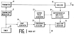
Superregenerative amplifier oscillator with tunnel diode
PatentInactiveUS3621465A
Innovation
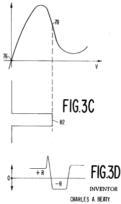
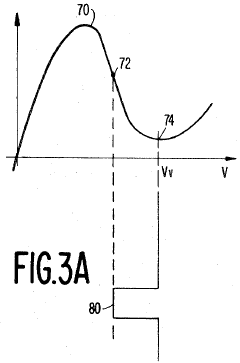
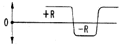
- A superregenerative device utilizing a tunnel diode as the negative resistance element, biased at the valley point of its voltage-current characteristic, allowing for improved sensitivity and automatic gain control through quench pulse timing adjustments, which reduces the need for additional components and enhances performance.
Straight-through r.f. microwave communications repeater system using tunnel diode amplifier for constant power output level
PatentInactiveUS3629706A
Innovation
- A straight-through RF microwave communications repeater system utilizing tunnel diode amplifiers provides constant power output over a wide range of input levels without distortion, reducing the number of components and using identical amplifier modules for reliability and ease of maintenance, enabling operation in higher frequency bands with reduced component count and distortion.
Performance Benchmarking and Testing Protocols
To establish a comprehensive evaluation framework for the Tunnel Diode technology integration, standardized performance benchmarking and testing protocols are essential. These protocols must address both the fundamental electrical characteristics of tunnel diodes and their performance in signal processing applications. The benchmarking methodology should begin with basic parameter measurements including peak-to-valley current ratio, switching speed, and noise characteristics under various temperature and voltage conditions.
For signal processing applications specifically, the testing protocol should incorporate measurements of signal-to-noise ratio (SNR) improvement, detection sensitivity thresholds, and response time across different frequency bands. Comparative analysis against conventional signal processing technologies such as standard diodes, transistor-based amplifiers, and digital signal processors provides necessary context for performance evaluation. These comparisons should be conducted using standardized signal inputs with varying complexity levels to assess real-world performance capabilities.
Environmental testing represents another critical dimension of the benchmarking protocol. Tunnel diode performance must be evaluated across temperature ranges from -40°C to 125°C, under various humidity conditions, and with exposure to electromagnetic interference. This environmental resilience testing is particularly important for applications in harsh operating environments such as industrial settings, aerospace, and defense systems where signal integrity is paramount.
Power efficiency metrics form a key component of the testing protocol, measuring power consumption per unit of signal processing capability. This includes standby power requirements, active processing power draw, and thermal management needs. The protocol should establish standardized measurement conditions to ensure reproducibility of results across different testing facilities and enable meaningful comparison between different tunnel diode implementations.
Reliability testing protocols must address long-term performance stability, mean time between failures (MTBF), and degradation characteristics under continuous operation. Accelerated life testing methodologies should be employed to predict operational lifespan in various application scenarios. Statistical analysis of performance variation across production batches is essential for quality assurance and manufacturing process optimization.
Integration testing protocols should evaluate the tunnel diode framework's compatibility with existing signal processing systems, focusing on interface requirements, signal conversion efficiency, and system-level performance improvements. These tests must quantify the practical benefits of tunnel diode integration in terms of overall system performance enhancement, implementation complexity, and cost-effectiveness compared to alternative solutions.
Semiconductor Manufacturing Considerations
The integration of tunnel diode frameworks into semiconductor manufacturing processes presents unique challenges and considerations that must be addressed to ensure optimal performance and reliability. The fabrication of tunnel diodes requires precise control over doping concentrations, as the tunneling effect depends critically on the formation of an extremely narrow depletion region between heavily doped p-type and n-type semiconductors. This necessitates advanced epitaxial growth techniques such as Molecular Beam Epitaxy (MBE) or Metal-Organic Chemical Vapor Deposition (MOCVD) to achieve the required atomic-level precision.
Material selection plays a crucial role in tunnel diode manufacturing. While traditional germanium-based tunnel diodes were common in early applications, modern signal processing demands have driven the development of III-V compound semiconductor-based devices, particularly those utilizing GaAs, InP, and their alloys. These materials offer superior electron mobility and can operate at higher frequencies, making them ideal for advanced signal insight applications.
Cleanroom environments for tunnel diode fabrication must maintain exceptionally high standards, typically Class 10 (ISO 4) or better, to prevent contamination that could disrupt the delicate tunneling mechanism. The lithography processes employed must achieve sub-micron resolution, often requiring electron beam lithography rather than conventional photolithography techniques to define the critical dimensions of these devices.
Thermal management during manufacturing represents another significant consideration. The performance characteristics of tunnel diodes are highly temperature-sensitive, and process temperatures must be carefully controlled to prevent dopant diffusion that could widen the junction and compromise the tunneling effect. Post-fabrication annealing procedures must be precisely calibrated to optimize device performance without degrading the junction properties.
Testing and quality control for tunnel diode integration present unique challenges. Standard semiconductor testing protocols must be supplemented with specialized measurements to verify the negative differential resistance (NDR) region that characterizes tunnel diode operation. This requires custom test fixtures and high-frequency measurement capabilities to accurately assess device performance under operational conditions.
Yield management for tunnel diode manufacturing typically falls below that of conventional semiconductor devices due to the stringent requirements for junction formation. Manufacturers must implement advanced statistical process control methods and in-line monitoring to identify and correct process deviations before they impact device performance. The integration of these specialized components into larger signal processing systems requires careful consideration of interface compatibility and signal integrity preservation.
Unlock deeper insights with Patsnap Eureka Quick Research — get a full tech report to explore trends and direct your research. Try now!
Generate Your Research Report Instantly with AI Agent
Supercharge your innovation with Patsnap Eureka AI Agent Platform!