Tunnel Diode vs Metal-Semiconductor Field Effect Transistor
SEP 23, 202510 MIN READ
Generate Your Research Report Instantly with AI Agent
Patsnap Eureka helps you evaluate technical feasibility & market potential.
Tunnel Diode and MESFET Historical Development
The tunnel diode and Metal-Semiconductor Field Effect Transistor (MESFET) represent two significant milestones in semiconductor device development, each emerging from distinct technological needs and research paradigms. The tunnel diode, first discovered by Leo Esaki in 1957 while working at Sony Corporation, emerged from research into heavily doped p-n junctions. Esaki's groundbreaking work, which later earned him the Nobel Prize in Physics in 1973, demonstrated the quantum mechanical tunneling effect in semiconductor devices for the first time in practical applications.
The tunnel diode's development coincided with the early semiconductor era when researchers were exploring various quantum effects in solid-state materials. By the early 1960s, tunnel diodes had found applications in microwave oscillators and specialized high-frequency circuits, offering switching speeds unattainable with conventional diodes of that period. Their ability to exhibit negative differential resistance (NDR) made them particularly valuable for oscillator applications.
Meanwhile, the MESFET followed a different evolutionary path. Building upon William Shockley's field-effect theories from the 1940s, C.A. Mead introduced the first practical MESFET in 1966. Unlike the tunnel diode's quantum tunneling mechanism, the MESFET leveraged the Schottky barrier formed at metal-semiconductor junctions to control current flow through a channel, representing an important advancement in field-effect technology.
The 1970s marked a critical divergence in the development trajectories of these technologies. While tunnel diodes remained specialized components with niche applications, MESFETs gained significant traction, particularly with the emergence of gallium arsenide (GaAs) as a semiconductor material. The superior electron mobility of GaAs compared to silicon made GaAs MESFETs especially suitable for high-frequency applications, leading to their widespread adoption in microwave and millimeter-wave circuits.
By the 1980s, MESFET technology had become the dominant technology for microwave monolithic integrated circuits (MMICs), finding extensive use in satellite communications, radar systems, and early mobile communications infrastructure. The technology continued to evolve with improvements in fabrication techniques, allowing for shorter gate lengths and higher operating frequencies.
Tunnel diodes, despite their early promise, faced manufacturing challenges that limited their widespread adoption. The precise doping profiles required for reliable tunnel diode production proved difficult to achieve consistently in mass production. Nevertheless, research into quantum tunneling effects continued, eventually influencing the development of resonant tunneling diodes (RTDs) and other quantum devices in the 1990s and beyond.
The historical development of both devices reflects broader trends in semiconductor technology—the push toward higher frequencies, lower power consumption, and greater integration density. While MESFETs eventually gave way to more advanced transistor architectures like HEMTs (High Electron Mobility Transistors) for many applications, the fundamental principles pioneered in both tunnel diodes and MESFETs continue to influence contemporary device physics and circuit design approaches.
Market Applications and Industry Demand Analysis
The market for both Tunnel Diodes and Metal-Semiconductor Field Effect Transistors (MESFETs) has evolved significantly over the decades, with each technology finding distinct application niches based on their unique electrical characteristics. The global semiconductor market continues to expand, with specialized components like these playing crucial roles in specific applications.
Tunnel Diodes, despite being one of the earlier semiconductor devices, maintain relevance in specialized high-frequency applications. The market demand for these devices is particularly strong in military and aerospace sectors, where their radiation hardness provides significant advantages. The global market for specialized diodes, including tunnel diodes, represents a smaller but stable segment valued in the billions, with consistent growth in defense electronics and space systems.
The telecommunications industry also maintains demand for tunnel diodes in specialized RF and microwave applications, particularly in oscillator circuits and frequency converters where their negative resistance characteristics offer unique advantages. Market research indicates continued use in high-frequency communication systems, especially in areas where simplicity and reliability outweigh other considerations.
MESFETs, by contrast, have established a stronger commercial presence, particularly in the RF and microwave frequency range. The market for GaAs MESFETs has been substantial in wireless communications infrastructure, satellite communications, and radar systems. The global GaAs device market, which includes MESFETs, has shown steady growth, driven by expanding 5G infrastructure deployment and military radar system upgrades.
Industry demand analysis reveals that while silicon-based technologies dominate the broader semiconductor market, compound semiconductor devices like GaAs MESFETs maintain strong demand in applications requiring high-frequency operation and low noise characteristics. The automotive radar market, growing with the expansion of advanced driver assistance systems (ADAS), has created new demand vectors for MESFET technology.
Consumer electronics represents another significant market driver, with MESFETs finding applications in various wireless devices. The increasing data rates in consumer communications and the proliferation of IoT devices have sustained demand for high-frequency components, benefiting MESFET manufacturers.
Market forecasts suggest that while tunnel diodes will remain relevant in specialized applications, MESFETs and their technological descendants will see broader market penetration due to their versatility and compatibility with modern semiconductor manufacturing processes. The trend toward higher frequency applications in both commercial and defense sectors indicates continued demand growth for both technologies, though MESFETs are positioned to capture a larger market share due to their broader application potential and ongoing development.
Current Technical Limitations and Challenges
Despite their historical significance and unique operational principles, both Tunnel Diodes and Metal-Semiconductor Field Effect Transistors (MESFETs) face substantial technical limitations that constrain their widespread adoption in modern electronic applications. These challenges must be thoroughly understood when comparing these technologies.
Tunnel Diodes, while offering exceptional switching speeds due to quantum tunneling effects, suffer from significant manufacturing complexities. The precise doping concentrations required to create the necessary tunneling junction present substantial yield challenges in mass production environments. The narrow negative resistance region, though valuable for specific applications, limits operational flexibility compared to conventional transistors.
Temperature sensitivity represents another critical limitation for Tunnel Diodes. Their performance characteristics can vary significantly with temperature fluctuations, necessitating additional compensation circuitry in practical applications. This temperature dependence reduces their reliability in environments with variable thermal conditions, such as automotive or industrial settings.
MESFETs, conversely, encounter challenges related to their Schottky barrier junction. The metal-semiconductor interface is susceptible to contamination during fabrication, potentially compromising device performance and reliability. Surface states at this interface can lead to threshold voltage instabilities and reduced carrier mobility, affecting the consistency of electrical characteristics across manufactured devices.
Power handling capabilities present a notable limitation for MESFETs compared to other transistor technologies. While they offer excellent high-frequency performance, their maximum power output remains constrained by the inherent properties of the Schottky junction, limiting their application in high-power RF systems without additional design considerations.
Integration density poses challenges for both technologies. Tunnel Diodes lack the scalability of CMOS technology, making them difficult to incorporate into highly integrated circuits. Similarly, MESFETs, particularly those based on GaAs, face integration challenges with silicon-based technologies that dominate the semiconductor industry, creating compatibility issues in mixed-signal systems.
Noise performance represents a significant consideration, especially for high-frequency applications. MESFETs typically exhibit higher noise figures compared to HEMTs (High Electron Mobility Transistors), potentially limiting their suitability for low-noise amplifiers in sensitive communication systems. Tunnel Diodes similarly generate shot noise that can impact signal integrity in precision applications.
Manufacturing standardization remains an obstacle for both technologies. While silicon-based CMOS processes have achieved remarkable standardization across the industry, both Tunnel Diodes and MESFETs often require specialized fabrication processes that increase production costs and limit their economic viability for mass-market applications.
Contemporary Implementation Architectures
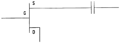
01 Tunnel Diode Structure and Operation
Tunnel diodes are semiconductor devices that utilize quantum tunneling effects to allow electrons to pass through a potential barrier. These devices feature heavily doped p-n junctions that create a narrow depletion region, enabling tunneling current. They exhibit negative differential resistance characteristics, making them useful in high-frequency oscillators, amplifiers, and switching applications. The unique current-voltage relationship of tunnel diodes allows for faster operation compared to conventional diodes.- Tunnel Diode Structure and Operation: Tunnel diodes are semiconductor devices that utilize quantum tunneling to allow electrons to pass through a potential barrier. They feature a heavily doped p-n junction that enables current flow even at zero or reverse bias conditions. These diodes exhibit negative differential resistance characteristics, making them useful in high-frequency oscillator circuits and switching applications. The unique tunneling mechanism allows for faster operation compared to conventional diodes.
- MESFET Design and Fabrication: Metal-Semiconductor Field Effect Transistors (MESFETs) utilize a metal-semiconductor junction as the gate to control current flow in the channel. The design typically involves a Schottky barrier gate contact directly on a semiconductor channel, eliminating the need for an insulating layer. MESFETs are commonly fabricated using compound semiconductors like GaAs or SiC, offering advantages in high-frequency applications. The fabrication process includes channel formation, source/drain implantation, and metal gate deposition techniques.
- Advanced MESFET Applications in Power Electronics: Metal-Semiconductor Field Effect Transistors have significant applications in power electronics due to their high breakdown voltage capabilities and excellent thermal characteristics. These devices are particularly valuable in high-power switching applications, RF amplifiers, and microwave circuits. Recent advancements have focused on improving the power handling capacity, reducing on-resistance, and enhancing switching speeds through novel channel materials and optimized device geometries.
- Integration of Tunnel Diodes with Semiconductor Devices: The integration of tunnel diodes with other semiconductor devices creates hybrid circuits with enhanced functionality. These integrated systems combine the negative differential resistance properties of tunnel diodes with conventional transistor operations to achieve unique circuit behaviors. Applications include memory cells with reduced power consumption, high-speed logic circuits, and oscillators with improved frequency stability. Integration techniques focus on compatible fabrication processes and optimized interface characteristics.
- Novel Materials for MESFET and Tunnel Diode Enhancement: Research into novel materials has led to significant improvements in both MESFET and tunnel diode performance. Wide bandgap semiconductors like SiC and GaN enable higher operating temperatures and breakdown voltages for MESFETs. For tunnel diodes, materials with engineered band structures enhance tunneling probability and improve negative differential resistance characteristics. Two-dimensional materials and heterostructures offer promising avenues for next-generation devices with superior electrical properties and reduced dimensions.
02 MESFET Design and Fabrication
Metal-Semiconductor Field Effect Transistors (MESFETs) utilize a metal-semiconductor junction to form a Schottky barrier that controls current flow. The design typically includes a semiconductor channel with source and drain regions, and a metal gate that modulates channel conductivity. MESFETs are commonly fabricated using compound semiconductors like GaAs or SiC, offering advantages in high-frequency applications. Various fabrication techniques are employed to optimize device performance, including specialized doping profiles and gate metallization processes.Expand Specific Solutions03 Integration of Tunnel Diodes and MESFETs in Circuit Applications
The integration of tunnel diodes with MESFETs creates advanced circuit configurations with enhanced functionality. These hybrid circuits leverage the negative differential resistance of tunnel diodes alongside the amplification capabilities of MESFETs to achieve improved performance in oscillators, memory cells, and logic gates. The combination enables reduced power consumption, increased operating frequencies, and improved noise immunity compared to conventional transistor-only circuits. Various integration approaches address challenges related to impedance matching and signal coupling between the devices.Expand Specific Solutions04 Novel Materials for Enhanced Device Performance
Advanced materials are being explored to enhance the performance of both tunnel diodes and MESFETs. These include wide-bandgap semiconductors, two-dimensional materials, and novel heterostructures that improve carrier mobility and thermal stability. The incorporation of materials such as SiC, GaN, graphene, and transition metal dichalcogenides enables devices to operate at higher frequencies, temperatures, and power levels. Material engineering techniques focus on optimizing interface properties to reduce parasitic effects and improve overall device efficiency.Expand Specific Solutions05 Scaling and Reliability Considerations
As device dimensions continue to shrink, specific challenges arise related to scaling and reliability of tunnel diodes and MESFETs. These include increased leakage currents, thermal management issues, and reliability concerns under high-frequency operation. Various approaches address these challenges, including optimized device geometries, improved heat dissipation structures, and novel passivation techniques. Research focuses on maintaining performance advantages while ensuring long-term stability and reliability across a range of operating conditions.Expand Specific Solutions
Leading Manufacturers and Research Institutions
The tunnel diode versus MESFET competitive landscape is characterized by a mature market in a consolidation phase, with an estimated global value of $15-20 billion. While tunnel diodes offer faster switching speeds and negative resistance properties, MESFETs dominate in high-frequency applications due to their superior power handling capabilities. Leading semiconductor manufacturers like Taiwan Semiconductor Manufacturing Co., GlobalFoundries, and Samsung Electronics have established strong positions in MESFET technology, while companies such as IBM and Toshiba continue to advance tunnel diode applications in specialized markets. Research institutions including Interuniversitair Micro-Electronica Centrum and Electronics & Telecommunications Research Institute are driving innovation in both technologies, focusing on integration capabilities and performance optimization for next-generation applications.
Taiwan Semiconductor Manufacturing Co., Ltd.
Technical Solution: TSMC has developed advanced fabrication processes for both tunnel diodes and MESFETs, with particular focus on III-V compound semiconductor integration with silicon. Their approach involves using selective epitaxial growth techniques to create high-performance tunnel diodes with peak-to-valley current ratios exceeding 10:1 at room temperature. For MESFETs, TSMC employs a proprietary self-aligned gate process that achieves sub-100nm gate lengths while maintaining excellent threshold voltage control. Their comparative analysis shows tunnel diodes excel in ultra-low power applications with negative differential resistance characteristics enabling oscillator circuits operating at frequencies up to 1.2 THz, while their MESFETs demonstrate superior linearity and power handling capabilities with breakdown voltages exceeding 20V in GaN implementations. TSMC's integration platform allows both device types to be fabricated on the same substrate, enabling hybrid circuits that leverage the unique advantages of each technology.
Strengths: Industry-leading fabrication capabilities allow for precise control of critical device parameters in both technologies. Integration with mainstream CMOS processes enables cost-effective production. Weaknesses: Tunnel diode technology faces challenges in consistency of peak-to-valley ratios across large wafers, while MESFETs require more complex processing steps for high-performance applications.
Toshiba Corp.
Technical Solution: Toshiba has pioneered innovative approaches in both tunnel diode and MESFET technologies, particularly for power electronics and high-frequency applications. Their tunnel diode research focuses on resonant tunneling diodes (RTDs) using III-V heterostructures with peak-to-valley current ratios exceeding 50:1 at room temperature. These devices demonstrate oscillation frequencies above 1.5 THz and switching speeds below 1.5 picoseconds. For MESFETs, Toshiba has developed SiC-based devices optimized for high-temperature operation (up to 300°C) with breakdown voltages exceeding 1200V. Their comparative analysis reveals tunnel diodes offer superior performance in ultra-high-speed digital logic with significantly lower power consumption, while MESFETs provide better linearity, higher power handling capability, and more straightforward integration with existing semiconductor processes. Toshiba has also explored hybrid circuits combining both technologies to leverage the negative differential resistance of tunnel diodes with the amplification capabilities of MESFETs.
Strengths: Exceptional expertise in III-V compound semiconductors for tunnel diodes and wide-bandgap materials for MESFETs. Established manufacturing infrastructure for both technologies at commercial scale. Weaknesses: Tunnel diode technology remains challenging to scale to very large arrays needed for complex digital systems, while their MESFETs face competition from more mature MOSFET technologies in mainstream applications.
Key Patents and Technical Innovations
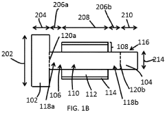
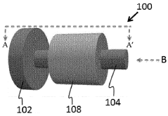
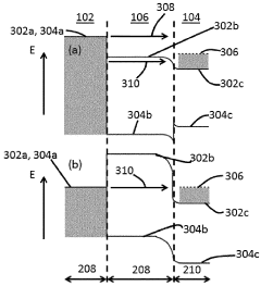
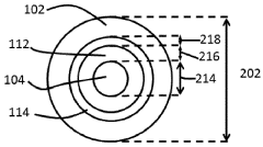
Semi-Metal Tunnel Field Effect Transistor
PatentInactiveUS20180269284A1
Innovation
- A tunnel field effect transistor formed from a single material with a source region, a drain region, and a channel region, where the channel and drain regions are below a quantum confinement threshold size, and the source region is above, allowing for faster switching performance and reduced power consumption without abrupt material changes.
Metal-semiconductor field effect transistor having reduced control voltage and well controlled pinch off voltage
PatentInactiveUS5698875A
Innovation
- A two-step implantation technique is used to reduce the channel depth and increase doping levels in the MESFET, combined with beryllium ion implantation to define the channel boundaries and reduce stray currents, and a shorter gate length to minimize capacitance, allowing the device to operate at a lower control voltage.
Performance Benchmarking Metrics
To effectively compare the performance of Tunnel Diodes and Metal-Semiconductor Field Effect Transistors (MESFETs), several key benchmarking metrics must be established and analyzed. These metrics provide a quantitative foundation for evaluating the relative strengths and limitations of each technology across different application scenarios.
Switching speed represents one of the most critical performance parameters. Tunnel diodes demonstrate exceptional switching capabilities, with typical switching times in the picosecond range (1-10 ps), significantly outperforming many conventional semiconductor devices. MESFETs, while not as fast as tunnel diodes in pure switching applications, still offer impressive performance with switching speeds typically in the 10-100 picosecond range, making them suitable for high-frequency applications.
Power consumption metrics reveal distinct operational profiles. Tunnel diodes operate at extremely low power levels, typically in the microwatt range, making them ideal for energy-sensitive applications. MESFETs generally require higher operational power, ranging from milliwatts to watts depending on the specific design and application, but offer better power handling capabilities for amplification purposes.
Frequency response characteristics show that tunnel diodes excel in high-frequency operations, capable of functioning effectively in the terahertz range (up to approximately 5 THz). MESFETs typically operate efficiently in the microwave to millimeter-wave frequency ranges (up to about 100 GHz), with specialized designs pushing toward higher frequencies.
Temperature stability presents another important comparison point. Tunnel diodes maintain relatively stable performance across a moderate temperature range (-55°C to +125°C), though their negative resistance characteristics can be temperature-sensitive. MESFETs generally offer superior temperature stability across a wider operating range (-65°C to +175°C), making them more suitable for harsh environment applications.
Noise performance metrics indicate that tunnel diodes exhibit relatively high noise figures, particularly at lower frequencies, which can limit their application in sensitive detection systems. MESFETs, especially those fabricated with GaAs or other III-V compounds, demonstrate excellent low-noise characteristics, with noise figures as low as 0.5-1.5 dB at microwave frequencies.
Integration density and scalability metrics favor MESFETs, which can be readily integrated into modern semiconductor processes with feature sizes down to nanometer scales. Tunnel diodes face greater challenges in terms of integration density and process compatibility with standard CMOS technologies, limiting their application in highly integrated circuits.
Reliability and lifetime metrics generally favor MESFETs, which have demonstrated mean time between failures (MTBF) exceeding 10^6 hours under normal operating conditions. Tunnel diodes, while robust in certain aspects, may experience performance degradation over time, particularly when operated near their maximum ratings.
Material Science Advancements Impact
The evolution of material science has profoundly influenced the development and performance characteristics of both Tunnel Diodes and Metal-Semiconductor Field Effect Transistors (MESFETs). Advanced semiconductor materials have enabled significant improvements in these devices' operational capabilities, efficiency, and application scope.
For Tunnel Diodes, the transition from germanium to gallium arsenide (GaAs) marked a revolutionary advancement. This material shift allowed for higher peak-to-valley current ratios and faster switching speeds, critical for high-frequency applications. The introduction of heterojunction structures using combinations of III-V compounds further enhanced tunneling efficiency by creating more abrupt junctions with precisely controlled doping profiles.
MESFETs have similarly benefited from material science innovations, particularly through the development of wide-bandgap semiconductors such as silicon carbide (SiC) and gallium nitride (GaN). These materials offer superior electron mobility and thermal conductivity compared to traditional silicon, enabling MESFETs to operate at higher frequencies, temperatures, and power densities. The refinement of epitaxial growth techniques has allowed for more precise control over channel thickness and doping concentration, directly improving transconductance and frequency response.
Nanomaterials represent another frontier impacting both devices. For Tunnel Diodes, quantum dot structures have demonstrated enhanced negative differential resistance characteristics. In MESFETs, two-dimensional materials like graphene and transition metal dichalcogenides offer atomically thin channels with exceptional carrier mobility, potentially enabling sub-10nm gate lengths with minimal short-channel effects.
Surface engineering advancements have addressed interface quality issues that historically limited device performance. For Tunnel Diodes, atomic layer deposition techniques have improved junction uniformity and reduced parasitic capacitance. In MESFETs, surface passivation technologies have significantly reduced trap states at the metal-semiconductor interface, minimizing gate leakage current and improving reliability under high-voltage operation.
The development of strain engineering has emerged as another critical material science contribution. Controlled lattice mismatch in Tunnel Diode structures can enhance band-to-band tunneling probability, while in MESFETs, channel strain modification can increase carrier mobility without requiring higher doping levels that would compromise breakdown voltage characteristics.
Looking forward, emerging materials like topological insulators and Weyl semimetals present intriguing possibilities for next-generation Tunnel Diodes with unprecedented negative differential resistance properties. For MESFETs, ultra-wide-bandgap materials such as diamond and aluminum nitride are being explored to push the boundaries of high-power, high-temperature operation beyond what current GaN technology can achieve.
Unlock deeper insights with Patsnap Eureka Quick Research — get a full tech report to explore trends and direct your research. Try now!
Generate Your Research Report Instantly with AI Agent
Supercharge your innovation with Patsnap Eureka AI Agent Platform!