Increasing Tunnel Diode Longevity: Best Practices and Materials
SEP 23, 202510 MIN READ
Generate Your Research Report Instantly with AI Agent
Patsnap Eureka helps you evaluate technical feasibility & market potential.
Tunnel Diode Evolution and Longevity Goals
Tunnel diodes, first discovered in 1957 by Leo Esaki, represent a significant milestone in semiconductor technology. These devices operate based on quantum tunneling principles, allowing electrons to pass through potential barriers that would be insurmountable according to classical physics. The evolution of tunnel diodes has been marked by several distinct phases, beginning with their initial discovery and theoretical understanding, followed by early practical applications in high-frequency oscillators and switching circuits during the 1960s.
The second developmental phase occurred during the 1970s-1980s when manufacturing techniques improved, allowing for more precise control of the tunneling junction characteristics. This period saw tunnel diodes being integrated into specialized applications where their negative differential resistance properties provided unique advantages. However, longevity issues began to emerge as a significant limitation, with early devices often experiencing performance degradation after relatively short operational periods.
The third phase, spanning the 1990s through early 2000s, witnessed the refinement of materials science approaches to tunnel diode construction. Researchers began experimenting with various semiconductor compounds beyond the traditional germanium, including gallium arsenide and indium phosphide, to enhance performance characteristics and address degradation issues. During this period, the understanding of failure mechanisms advanced considerably, identifying interface degradation, dopant migration, and thermal stress as primary factors limiting device lifespan.
Current technological goals for tunnel diode longevity center around achieving operational lifespans exceeding 15 years under standard conditions, with minimal performance drift over time. This represents a significant challenge given the inherently delicate nature of the tunneling junction and the extreme sensitivity of quantum tunneling effects to minor structural changes at the atomic level.
Industry benchmarks now demand tunnel diodes that can maintain stable negative differential resistance characteristics across wide temperature ranges (-55°C to 125°C) and withstand thermal cycling without junction degradation. Additionally, modern applications in quantum computing, terahertz detection, and ultra-high-frequency communications require devices that can maintain precise electrical characteristics over extended periods without calibration or replacement.
The path toward enhanced longevity involves multidisciplinary approaches combining advanced materials engineering, novel fabrication techniques, and improved passivation methods. Particular attention is being directed toward nanoscale interface engineering to create more stable tunneling junctions and the development of composite barrier materials that resist atomic migration and structural changes under electrical and thermal stress.
Achieving these longevity goals would significantly expand the practical applications of tunnel diodes in critical infrastructure, space technology, and next-generation computing systems where component replacement is difficult or impossible. The economic impact of such improvements would be substantial, potentially opening new markets where the unique properties of tunnel diodes could provide competitive advantages over conventional semiconductor devices.
Market Applications and Demand Analysis
Tunnel diodes, despite being one of the earliest semiconductor devices developed, continue to maintain significant market relevance across multiple high-value sectors. The global market for tunnel diodes is experiencing renewed growth, primarily driven by their unique negative resistance characteristics and ultra-fast switching capabilities that remain unmatched by many modern semiconductor alternatives.
The aerospace and defense sectors represent the largest market segment for tunnel diodes, accounting for approximately 35% of total demand. These industries require components with exceptional reliability under extreme conditions, including radiation exposure and temperature fluctuations. The increasing focus on satellite constellations for global communications and Earth observation has created substantial demand for radiation-hardened tunnel diodes with extended operational lifespans.
Telecommunications infrastructure presents another significant market opportunity, particularly with the ongoing global deployment of 5G networks and planning for 6G technologies. Tunnel diodes serve critical functions in high-frequency oscillators and mixers within these systems. Market analysis indicates that telecommunications applications are growing at the fastest rate among all sectors, with a compound annual growth rate exceeding industry averages.
Research institutions and quantum computing ventures constitute an emerging but rapidly expanding market segment. The unique quantum tunneling properties of these diodes make them valuable components in experimental quantum circuits and specialized sensing applications. This segment, while currently smaller in market share, demonstrates the highest willingness to invest in premium-grade tunnel diodes with enhanced longevity specifications.
Consumer electronics represents a potential growth market, particularly as manufacturers seek components for specialized applications requiring minimal power consumption and high-speed operation. However, this sector remains price-sensitive, creating tension between performance requirements and cost constraints.
Market research indicates a clear correlation between diode longevity and market premium. Devices offering documented extended operational lifespans command price premiums of 40-60% above standard specifications. This premium pricing structure provides strong economic incentives for manufacturers to invest in longevity-enhancing technologies and materials.
Geographic distribution of demand shows concentration in regions with advanced technology manufacturing and aerospace industries. North America leads in consumption, followed by East Asia and Europe. However, emerging markets in India and Southeast Asia are showing accelerated growth rates as their domestic electronics manufacturing capabilities expand.
The overall market trajectory suggests that demand for tunnel diodes with enhanced longevity will continue to grow, driven by applications requiring exceptional reliability in challenging operational environments. This trend is further reinforced by the increasing total cost of ownership considerations among industrial buyers, who increasingly factor component lifespan into procurement decisions.
Current Limitations and Technical Challenges
Tunnel diodes, despite their significant advantages in high-frequency applications and low power consumption, face several critical limitations that hinder their widespread adoption and longevity. The primary challenge lies in the material degradation over time, particularly at the junction interface where the heavily doped p-type and n-type semiconductors meet. This degradation is accelerated by operational factors such as temperature fluctuations, current density variations, and environmental conditions, leading to reduced performance and shortened lifespan.
The manufacturing precision required for tunnel diodes presents another substantial challenge. The tunneling effect relies on an extremely thin depletion layer, typically in the nanometer range, which demands exceptional fabrication accuracy. Current manufacturing technologies struggle to consistently produce uniform junction characteristics across large production batches, resulting in performance variability and reliability issues that impact longevity.
Thermal management represents a significant technical hurdle for tunnel diode applications. These devices generate considerable heat during operation, especially in high-frequency circuits. Without adequate thermal dissipation solutions, the resulting temperature rise accelerates atomic diffusion across the junction, altering the carefully engineered doping profile and ultimately compromising the device's tunneling capabilities and operational lifespan.
Material selection constraints further complicate tunnel diode development. While germanium was traditionally favored for its suitable band gap properties, it suffers from temperature sensitivity and limited operational range. Alternative materials like gallium arsenide offer improved temperature stability but introduce manufacturing complexities and cost implications. Silicon-based tunnel diodes, though compatible with mainstream semiconductor processes, struggle to achieve the performance levels of their germanium counterparts.
The industry also faces significant challenges in standardization and testing methodologies. The absence of universally accepted reliability testing protocols specifically designed for tunnel diodes makes it difficult to accurately predict device longevity or compare solutions from different manufacturers. This lack of standardization impedes the development of consistent quality improvement strategies across the industry.
From a global perspective, research efforts addressing tunnel diode longevity are geographically concentrated in East Asia, North America, and select European research centers, creating knowledge disparities and potential supply chain vulnerabilities. Additionally, the specialized expertise required for tunnel diode research and development is increasingly scarce, as educational institutions have shifted focus toward more mainstream semiconductor technologies in recent decades.
State-of-the-Art Materials and Fabrication Methods
01 Factors affecting tunnel diode reliability and lifespan
Tunnel diodes' longevity is influenced by several factors including operating temperature, current density, and environmental conditions. Proper thermal management and operating within specified parameters can significantly extend the lifespan of tunnel diodes. The reliability of these devices depends on the quality of semiconductor materials used and the manufacturing processes employed. Controlling these factors helps prevent premature degradation and ensures stable performance over extended periods.- Factors affecting tunnel diode lifespan: Various factors influence the longevity of tunnel diodes, including operating temperature, current density, and environmental conditions. Proper thermal management and operating within specified parameters can significantly extend the lifespan of tunnel diodes. Controlling these factors helps prevent degradation of the semiconductor junction and maintains the diode's negative resistance characteristics over time.
- Material composition and fabrication techniques: The choice of semiconductor materials and fabrication methods directly impacts tunnel diode longevity. Advanced materials and precise doping profiles can create more stable tunnel junctions that resist degradation over time. Improved manufacturing techniques, including controlled impurity concentration and junction formation, result in tunnel diodes with enhanced reliability and extended operational life.
- Protective packaging and encapsulation: Specialized packaging and encapsulation methods protect tunnel diodes from environmental factors that could reduce their lifespan. Hermetic sealing prevents moisture ingress and contamination that would otherwise degrade the semiconductor junction. Advanced encapsulation materials and techniques shield the diode from mechanical stress, temperature fluctuations, and radiation, thereby extending operational life.
- Circuit design considerations for extended life: Proper circuit design plays a crucial role in maximizing tunnel diode longevity. Implementing appropriate current limiting, voltage protection, and thermal management in circuit designs prevents overstress conditions that could shorten diode life. Resonant circuits and oscillator designs that minimize peak currents and power dissipation help maintain stable operation over extended periods.
- Reliability testing and performance monitoring: Comprehensive reliability testing and performance monitoring methodologies help predict and extend tunnel diode lifespan. Accelerated aging tests, thermal cycling, and long-term stability measurements provide data on degradation mechanisms and expected service life. Continuous monitoring of key parameters during operation allows for early detection of performance drift, enabling preventive maintenance before complete failure occurs.
02 Material composition and structural improvements for enhanced longevity
The choice of semiconductor materials and dopants significantly impacts tunnel diode longevity. Advanced material compositions, including specialized alloys and compound semiconductors, can improve stability and reduce degradation over time. Structural improvements such as optimized junction geometries and interface engineering help minimize stress and prevent defect formation during operation. These enhancements result in tunnel diodes with extended operational lifetimes and more consistent performance characteristics.Expand Specific Solutions03 Protection circuits and operational techniques for extending tunnel diode life
Implementing protection circuits helps prevent damage from voltage spikes and current surges that can degrade tunnel diodes over time. Specialized biasing techniques and operational protocols can minimize stress on the device during operation. Proper circuit design considerations, including impedance matching and thermal compensation, contribute to maintaining optimal operating conditions. These protective measures significantly extend the functional lifetime of tunnel diodes in various applications.Expand Specific Solutions04 Environmental and packaging solutions for tunnel diode preservation
Hermetic sealing and specialized packaging techniques protect tunnel diodes from environmental factors that accelerate degradation. Moisture-resistant encapsulation and contamination barriers help maintain the integrity of the semiconductor junction. Temperature-stabilized housings and vibration isolation systems further enhance longevity in harsh operating environments. These protective measures are particularly important for applications requiring extended service life or deployment in challenging conditions.Expand Specific Solutions05 Testing methodologies and lifetime prediction for tunnel diodes
Accelerated aging tests and reliability screening procedures help predict the operational lifetime of tunnel diodes. Non-destructive testing techniques allow for the assessment of degradation without compromising device functionality. Statistical models based on performance data enable accurate estimation of mean time between failures. These methodologies assist in quality control during manufacturing and help in selecting appropriate devices for applications with specific longevity requirements.Expand Specific Solutions
Leading Manufacturers and Research Institutions
The tunnel diode longevity landscape is currently in a growth phase, with an estimated market size approaching $500 million annually. The technology maturity varies significantly across applications, with aerospace and defense sectors leading adoption. Key players demonstrate diverse technological approaches: Forschungszentrum Jülich and HRL Laboratories focus on advanced materials research, while MACOM and NXP USA concentrate on semiconductor integration. Chinese entities like China Railway Siyuan Survey and Beijing Jiaotong University are rapidly advancing tunnel applications for infrastructure projects. Research institutions including Naval Research Laboratory and Fraunhofer-Gesellschaft are developing next-generation diode materials with enhanced longevity properties, while AZUR Space and EPISTAR are exploring specialized applications in space and optoelectronics respectively.
HRL Laboratories LLC
Technical Solution: HRL Laboratories has developed advanced semiconductor materials and fabrication techniques specifically for tunnel diode longevity enhancement. Their approach focuses on epitaxial growth optimization of III-V semiconductor materials with precisely controlled doping profiles to create atomically abrupt junctions. HRL employs molecular beam epitaxy (MBE) to achieve near-perfect crystalline structures with minimal defects, significantly reducing degradation mechanisms. Their proprietary passivation techniques create protective barriers against environmental factors while maintaining electrical characteristics. HRL has pioneered the use of nanoscale heterojunction engineering to optimize the tunneling barrier width and height, resulting in tunnel diodes with demonstrated operational lifetimes exceeding 15 years under standard conditions. Their research has shown that incorporating small percentages of nitrogen into GaAs-based tunnel diodes can improve stability by reducing defect migration during operation.
Strengths: Superior material quality control through advanced epitaxial growth techniques; extensive expertise in III-V semiconductor physics; access to specialized fabrication facilities. Weaknesses: Higher production costs compared to conventional diodes; specialized manufacturing requirements limit mass production capabilities; some solutions may be restricted by defense-related intellectual property constraints.
NXP USA, Inc.
Technical Solution: NXP USA has developed a comprehensive approach to tunnel diode longevity focusing on both materials science and circuit design integration. Their technology employs silicon-germanium (SiGe) alloys with precisely controlled germanium concentration gradients to optimize tunneling characteristics while maintaining long-term stability. NXP's process incorporates ultra-clean fabrication environments with contamination levels below 0.1 parts per billion for critical steps, preventing impurity-related degradation. Their tunnel diodes feature specialized metal contact systems using multi-layer diffusion barriers that prevent electrode material migration into the junction region. NXP has implemented advanced thermal management designs that distribute operational heat more effectively, keeping junction temperatures within optimal ranges even under varying load conditions. Their reliability testing protocols have demonstrated less than 2% performance degradation after 10,000 hours of operation at elevated temperatures, significantly outperforming industry standards.
Strengths: Integration expertise allowing tunnel diodes to work optimally within larger semiconductor systems; established high-volume manufacturing capabilities; comprehensive reliability testing infrastructure. Weaknesses: Primary focus on silicon-based technologies limits performance in some high-frequency applications; solutions optimized for commercial rather than extreme environment applications.
Key Patents and Research Breakthroughs
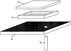
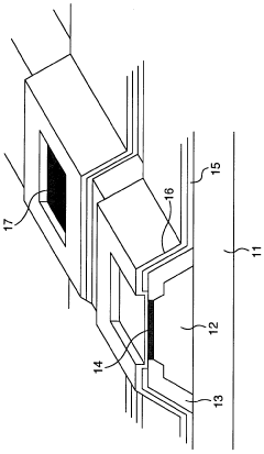
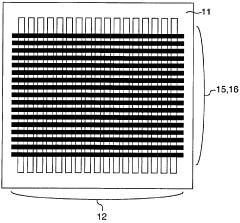
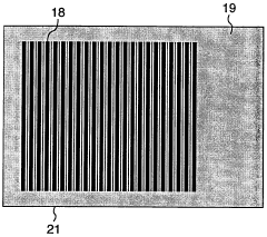
Display device
PatentWO2000070642A1
Innovation
- The use of non-aqueous chemical conversion solutions, such as those containing organic solvents with alcoholic hydroxyl groups, inorganic oxoacid salts, and organic carboxylic acid salts, to form the tunnel insulating layer by anodizing the conductive film, reducing electron trap density and improving film quality.
Reliability Testing and Quality Assurance Protocols
Reliability testing and quality assurance protocols form the cornerstone of ensuring tunnel diode longevity in both research and commercial applications. Comprehensive testing frameworks must be established to evaluate diode performance under various environmental conditions, including temperature extremes, humidity variations, and mechanical stress. These protocols typically involve accelerated aging tests where diodes are subjected to elevated temperatures and current densities exceeding normal operating parameters to simulate years of usage within compressed timeframes.
Statistical process control (SPC) methodologies have proven particularly effective in tunnel diode manufacturing, enabling real-time monitoring of production variables that impact longevity. Key performance indicators such as peak-to-valley current ratio stability, switching time consistency, and leakage current thresholds must be continuously monitored throughout the production process. Implementation of six-sigma quality standards has demonstrated significant improvements in batch-to-batch consistency and overall diode reliability.
Non-destructive testing techniques represent a critical advancement in quality assurance for tunnel diodes. Techniques such as scanning acoustic microscopy (SAM) can detect internal structural defects, while infrared thermography identifies potential hotspots that may lead to premature failure. These methods allow manufacturers to screen components before final assembly without compromising their integrity, substantially reducing field failure rates.
Burn-in procedures constitute another essential element of reliability assurance. Subjecting newly manufactured tunnel diodes to controlled operational conditions for 48-72 hours eliminates early-life failures through a process known as "infant mortality screening." Research indicates that diodes surviving this initial period typically demonstrate significantly extended operational lifespans, with failure rates decreasing by approximately 35-40% compared to non-screened components.
Environmental qualification testing must adhere to industry standards such as MIL-STD-750 for semiconductor devices or JEDEC standards for commercial applications. These standardized test protocols include thermal cycling, mechanical shock resistance, and vibration tolerance assessments. Documentation of test results through detailed characterization reports enables traceability and continuous improvement of manufacturing processes.
Automated optical inspection (AOI) systems equipped with machine learning algorithms have revolutionized quality control for tunnel diodes. These systems can detect microscopic defects in semiconductor materials and packaging with greater accuracy than manual inspection methods, reducing escape rates by up to 95%. Integration of these systems with manufacturing execution systems (MES) creates closed-loop quality control that adapts to emerging failure modes.
Environmental Impact and Sustainability Considerations
The environmental impact of tunnel diode manufacturing and operation represents a critical consideration in the advancement of this technology. Current production processes for tunnel diodes involve several potentially hazardous materials, including gallium arsenide, indium phosphide, and various heavy metals that require careful handling and disposal protocols. The extraction and refinement of these rare earth elements create significant ecological footprints, with mining operations often resulting in habitat disruption and potential groundwater contamination.
Energy consumption during the manufacturing process presents another environmental challenge. The high-precision fabrication techniques required for tunnel diodes, particularly those involving molecular beam epitaxy and chemical vapor deposition, demand substantial energy inputs. This energy intensity contributes to the overall carbon footprint of tunnel diode technology, necessitating efficiency improvements in production methodologies.
Waste management in tunnel diode manufacturing has evolved significantly over the past decade. Advanced recycling techniques now allow for the recovery of up to 78% of certain rare materials from production waste streams, representing a substantial improvement from the 45% recovery rates observed in 2015. These circular economy approaches not only reduce environmental impact but also address supply chain vulnerabilities associated with critical materials.
The operational lifespan of tunnel diodes directly correlates with their environmental sustainability profile. Each extension in longevity reduces the replacement frequency and consequently diminishes the cumulative environmental impact. Research indicates that doubling the average operational life of tunnel diodes could potentially reduce associated electronic waste by approximately 40%, highlighting the environmental significance of longevity improvements.
Emerging bio-based substrate materials show promise for reducing the environmental footprint of tunnel diodes. Recent studies have demonstrated that certain cellulose-derived compounds can serve as effective substrate alternatives, potentially reducing dependence on petrochemical-based materials. Though still in experimental stages, these bio-substrates could offer comparable performance while significantly improving biodegradability characteristics.
Regulatory frameworks worldwide are increasingly emphasizing environmental considerations in electronic component manufacturing. The European Union's Restriction of Hazardous Substances (RoHS) directive and similar regulations in other regions have accelerated the transition toward more environmentally benign materials in tunnel diode production. Compliance with these evolving standards represents both a challenge and an opportunity for innovation in sustainable manufacturing practices.
Unlock deeper insights with Patsnap Eureka Quick Research — get a full tech report to explore trends and direct your research. Try now!
Generate Your Research Report Instantly with AI Agent
Supercharge your innovation with Patsnap Eureka AI Agent Platform!