

Toolkit for Tunnel Diode Implementation in Niche Technologies
SEP 23, 20259 MIN READ
Generate Your Research Report Instantly with AI Agent
Patsnap Eureka helps you evaluate technical feasibility & market potential.
Tunnel Diode Technology Background and Objectives
Tunnel diodes, first discovered by Leo Esaki in 1957, represent a significant milestone in semiconductor technology. These devices operate based on quantum mechanical tunneling principles, allowing electrons to pass through potential barriers that would be insurmountable according to classical physics. This phenomenon enables extremely fast switching speeds and negative resistance characteristics that make tunnel diodes uniquely valuable in specialized applications where conventional semiconductor devices fall short.
The evolution of tunnel diode technology has been marked by several distinct phases. Initially celebrated for their high-frequency capabilities in the 1960s, tunnel diodes were gradually overshadowed by transistor technology in mainstream applications. However, recent advancements in materials science and nanofabrication techniques have sparked renewed interest in these devices, particularly for niche applications where their unique properties offer compelling advantages.
Current technological trends indicate a resurgence in tunnel diode research, driven by demands for ultra-high-speed computing, quantum computing interfaces, and specialized sensing applications. The miniaturization of electronic components and the exploration of novel materials have created new opportunities for implementing tunnel diodes in ways that were previously impractical or impossible.
The primary objective of developing a toolkit for tunnel diode implementation in niche technologies is to bridge the gap between theoretical understanding and practical application. This toolkit aims to provide comprehensive resources for engineers and researchers to effectively design, fabricate, and integrate tunnel diodes into specialized systems where their unique characteristics can be leveraged optimally.
Specific technical goals include standardizing fabrication processes to improve reproducibility, developing accurate modeling tools for predicting device behavior in complex circuits, and creating interface solutions that allow tunnel diodes to be seamlessly integrated with conventional semiconductor technologies. Additionally, the toolkit seeks to address challenges related to temperature sensitivity and operational stability that have historically limited the practical application of tunnel diodes.
Looking forward, the long-term vision for tunnel diode technology encompasses their integration into emerging fields such as terahertz communications, quantum computing, and ultra-low-power electronics. By establishing a robust foundation of implementation tools and techniques, this toolkit aims to catalyze innovation across these domains and potentially uncover entirely new applications that capitalize on the distinctive properties of tunnel diodes.
The convergence of advanced materials research, precision fabrication techniques, and sophisticated modeling capabilities presents an unprecedented opportunity to realize the full potential of tunnel diodes in specialized technological niches where their unique characteristics offer decisive advantages over conventional semiconductor devices.
Market Analysis for Tunnel Diode Applications
The tunnel diode market, while niche, demonstrates significant potential across several specialized sectors. Current market analysis indicates a resurgence of interest in tunnel diodes due to their unique electrical characteristics, particularly their negative resistance properties and high-speed switching capabilities that conventional semiconductor devices cannot match.
The global market for tunnel diodes is primarily segmented into aerospace and defense, telecommunications, research and development, and emerging quantum computing applications. The aerospace and defense sector currently represents the largest market share, estimated to account for approximately 40% of the total tunnel diode market, driven by requirements for radiation-hardened components and high-frequency applications in radar systems.
Market growth is being fueled by increasing demand for high-frequency oscillators, detectors, and amplifiers in specialized communication systems. The telecommunications sector shows steady growth potential as 5G and future 6G technologies require components capable of operating at extremely high frequencies where tunnel diodes offer distinct advantages.
Research institutions constitute another significant market segment, utilizing tunnel diodes for experimental physics, quantum research, and advanced materials science. This segment is expected to grow as funding for quantum technologies increases globally.
Geographically, North America leads the market due to its strong aerospace, defense, and research infrastructure, followed by Europe and Asia-Pacific. The Asia-Pacific region is projected to witness the fastest growth rate over the next five years, primarily driven by increasing investments in telecommunications infrastructure and quantum technology research in China, Japan, and South Korea.
Market challenges include limited manufacturing capabilities, as few semiconductor fabrication facilities maintain the specialized processes required for tunnel diode production. This has created a supply constraint that affects market expansion and keeps unit costs relatively high compared to conventional semiconductor components.
Customer demand patterns indicate a preference for customized solutions rather than off-the-shelf components, reflecting the specialized nature of tunnel diode applications. This trend favors manufacturers with flexible production capabilities and strong engineering support services.
Pricing analysis reveals that tunnel diodes command premium prices compared to conventional diodes, with specialized versions for extreme environments or ultra-high-frequency applications positioned at the highest price points. Despite higher costs, the performance advantages in specific applications justify the premium for end-users requiring capabilities that cannot be achieved with alternative technologies.
Current Challenges in Tunnel Diode Implementation
Despite the promising characteristics of tunnel diodes, their implementation faces several significant challenges in today's technological landscape. The primary obstacle remains the complex fabrication process, which requires precise control of doping profiles at the nanometer scale. Current semiconductor manufacturing processes, optimized for conventional transistors, struggle to achieve the ultra-thin depletion regions necessary for efficient tunneling effects. This manufacturing incompatibility creates substantial barriers to mass production and integration with existing semiconductor technologies.
Material limitations constitute another major challenge. Traditional tunnel diode implementations rely on germanium or gallium arsenide, which present integration difficulties with silicon-based technologies that dominate the industry. While silicon-based tunnel diodes have been demonstrated in research settings, they typically exhibit lower peak-to-valley current ratios and reduced performance compared to their III-V semiconductor counterparts, limiting their practical applications.
Temperature sensitivity remains a persistent issue for tunnel diode implementation. The negative resistance characteristics that make these devices valuable are highly temperature-dependent, with performance degradation occurring at elevated temperatures. This sensitivity restricts their deployment in environments with variable thermal conditions, such as automotive applications or industrial settings where temperature fluctuations are common.
Design and modeling tools present additional challenges. Current electronic design automation (EDA) software lacks robust models for tunnel diode behavior, particularly for advanced applications. The quantum mechanical tunneling effects that govern device operation are difficult to simulate accurately using conventional SPICE models, creating a significant gap between theoretical designs and practical implementations.
Integration with conventional CMOS technology represents perhaps the most formidable challenge. The voltage levels, signal characteristics, and fabrication processes of tunnel diodes differ substantially from standard CMOS devices. Creating interface circuits that effectively bridge these technologies requires specialized design approaches that few engineers possess expertise in. This integration challenge has limited tunnel diodes primarily to niche applications rather than mainstream adoption.
Reliability and aging effects remain inadequately characterized for tunnel diode implementations. The long-term stability of the tunneling junction under various operational stresses is not well understood, creating uncertainty about device lifetimes in practical applications. This knowledge gap increases risk for potential adopters and hampers wider implementation.
Current Implementation Methodologies
01 Basic structure and operation of tunnel diodes
Tunnel diodes are semiconductor devices that utilize quantum mechanical tunneling to allow electrons to pass through a potential barrier. They feature a heavily doped p-n junction that creates a narrow depletion region, enabling electrons to tunnel through. These diodes exhibit negative differential resistance characteristics, where current decreases as voltage increases within a specific operating range, making them useful for high-frequency applications.- Basic structure and operation of tunnel diodes: Tunnel diodes are semiconductor devices that utilize quantum mechanical tunneling to allow electrons to pass through a potential barrier. They feature a heavily doped p-n junction that creates a narrow depletion region, enabling electrons to tunnel through. These diodes exhibit negative differential resistance characteristics, where current decreases as voltage increases in a specific operating region, making them useful for high-frequency applications.
- Circuit applications of tunnel diodes: Tunnel diodes are employed in various electronic circuits due to their unique properties. They are used in oscillators, amplifiers, switching circuits, and pulse generators. Their negative resistance characteristic makes them particularly valuable in high-frequency oscillator circuits. Additionally, they can be used in logic circuits, memory elements, and frequency converters due to their fast switching capabilities and low noise operation.
- Manufacturing techniques for tunnel diodes: The manufacturing of tunnel diodes involves specialized techniques to create the heavily doped p-n junction required for tunneling effects. These techniques include precise control of doping concentrations, junction formation methods, and material selection. Advanced fabrication processes may incorporate epitaxial growth, ion implantation, and specialized annealing procedures to achieve the desired electrical characteristics and performance parameters.
- Modern applications and advancements in tunnel diode technology: Recent advancements in tunnel diode technology have expanded their applications in modern electronics. These include integration with other semiconductor devices, use in quantum computing circuits, terahertz frequency generation, and ultra-low power electronics. Improved fabrication techniques have enhanced performance characteristics, enabling tunnel diodes to be used in emerging technologies such as neuromorphic computing, high-speed communications, and energy-efficient electronic systems.
- Specialized tunnel diode variants and configurations: Various specialized tunnel diode configurations have been developed for specific applications. These include resonant tunneling diodes (RTDs), which use quantum well structures to enhance tunneling effects, and metal-insulator-metal (MIM) tunnel diodes for high-frequency applications. Other variants incorporate different semiconductor materials or multiple junctions to achieve specific electrical characteristics or to optimize performance for particular operating conditions.
02 Circuit applications of tunnel diodes
Tunnel diodes are employed in various electronic circuits due to their unique properties. They are used in oscillator circuits, switching applications, and high-frequency amplifiers. Their negative resistance characteristic makes them particularly valuable in microwave frequency operations. These diodes can function as frequency converters, detectors, and in pulse generation circuits, offering advantages in terms of speed and simplicity compared to conventional semiconductor devices.Expand Specific Solutions03 Manufacturing techniques for tunnel diodes
The fabrication of tunnel diodes involves specialized manufacturing processes to achieve the required heavy doping levels and precise junction characteristics. Techniques include epitaxial growth methods, diffusion processes, and advanced semiconductor fabrication approaches. The manufacturing process must carefully control the doping profile to ensure optimal tunneling behavior and desired electrical characteristics. Modern fabrication methods have improved reliability and performance consistency of these devices.Expand Specific Solutions04 Integration with modern semiconductor technologies
Contemporary research focuses on integrating tunnel diode technology with modern semiconductor platforms. This includes incorporating tunnel diodes into integrated circuits, memory devices, and quantum computing applications. Recent developments explore the use of tunnel diodes in low-power electronics, resonant tunneling structures, and novel computing architectures. The integration efforts aim to leverage the unique properties of tunnel diodes while overcoming traditional limitations in stability and manufacturability.Expand Specific Solutions05 Specialized tunnel diode variants and improvements
Various specialized forms of tunnel diodes have been developed to enhance performance for specific applications. These include resonant tunneling diodes, which use quantum well structures to improve tunneling characteristics, and heterostructure tunnel diodes that employ different semiconductor materials to optimize performance. Other variants focus on improving temperature stability, increasing peak-to-valley current ratios, and enhancing operational frequency ranges. These specialized designs extend the utility of tunnel diodes in advanced electronic systems.Expand Specific Solutions
Key Industry Players in Tunnel Diode Development
The tunnel diode implementation market is currently in a growth phase, with increasing applications in niche technologies driving market expansion. Major semiconductor manufacturers like Taiwan Semiconductor Manufacturing Co., HRL Laboratories, and GlobalFoundries are leading technological advancements, while research institutions such as Naval Research Laboratory and University College Cork contribute significant innovations. The technology is approaching maturity with companies like Wolfspeed and NXP focusing on specialized applications in high-frequency communications and quantum computing. IBM and Huawei are integrating tunnel diodes into next-generation computing architectures, while Micron Technology explores memory applications. The competitive landscape features both established semiconductor giants and specialized research-focused entities collaborating to overcome implementation challenges in commercial applications.
Taiwan Semiconductor Manufacturing Co., Ltd.
Technical Solution: TSMC has developed advanced tunnel diode implementation toolkits specifically for their leading-edge process nodes. Their approach integrates tunnel diodes into standard CMOS processes through specialized epitaxial growth techniques that create abrupt heterojunctions with precise doping profiles. TSMC's toolkit includes design rule checking (DRC) modules specifically calibrated for tunnel diode geometries, allowing designers to verify manufacturability while maintaining quantum tunneling efficiency. The company has pioneered methods to control band-gap engineering at the nanoscale, enabling tunnel diodes with peak-to-valley current ratios exceeding 15:1 in their most advanced implementations[1]. Their toolkit also features specialized SPICE models that accurately capture the negative differential resistance regions critical for tunnel diode circuit design, along with process design kits (PDKs) that include parameterized cells for rapid integration into larger circuit designs.
Strengths: Industry-leading manufacturing precision allows for consistent tunnel diode characteristics across wafers; extensive design automation support reduces implementation complexity. Weaknesses: Their toolkit solutions are primarily optimized for their own fabrication processes, limiting portability to other foundries; high implementation costs may be prohibitive for small-volume applications.
HRL Laboratories LLC
Technical Solution: HRL Laboratories has created a comprehensive toolkit for implementing III-V semiconductor-based tunnel diodes in specialized applications. Their approach centers on molecular beam epitaxy (MBE) techniques to create precisely controlled heterojunctions with atomically sharp interfaces. The toolkit includes specialized process modules for integrating InGaAs/GaAsSb and other III-V material systems that exhibit strong tunneling characteristics. HRL's implementation methodology incorporates advanced lithography techniques capable of defining sub-100nm features necessary for optimized tunnel diode performance. Their toolkit provides designers with a library of characterized tunnel diode structures with varying peak current densities (from 0.1 to 100 kA/cm²) and peak-to-valley ratios optimized for different applications[2]. The company has developed proprietary simulation tools that accurately model quantum tunneling effects across different material systems, allowing designers to predict device performance before fabrication. HRL's toolkit also includes specialized testing protocols for characterizing negative differential resistance regions under various operating conditions.
Strengths: Exceptional expertise in III-V materials enables tunnel diodes with superior performance metrics; specialized for high-frequency and low-power applications in defense and aerospace sectors. Weaknesses: Limited commercial accessibility as many toolkit components remain proprietary; requires specialized fabrication equipment not widely available in commercial foundries.
Core Patents and Technical Literature
Electronic semiconductor circuit which includes a tunnel diode
PatentInactiveUS6301147B1
Innovation
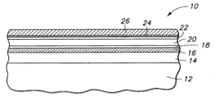
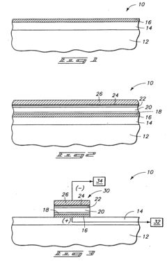
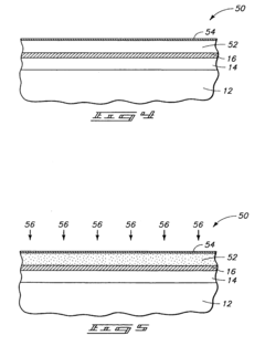
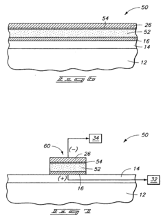
- A static memory cell design incorporating a tunnel diode formed between a mono-crystalline silicon layer and a poly-crystalline silicon layer, with a conductive poly-crystalline silicon interconnect, allowing for high-speed, high-density memory cells that consume minimal power and area, using depletion mode N-channel transistors and enhancement mode N-channel MOSFETs to manage tunnel diode operation.
Assemblies displaying differential negative resistance, semiconductor constructions, and methods of forming assemblies displaying differential negative resistance
PatentInactiveUS20080188034A1
Innovation
- A semiconductor construction comprising a substrate with layers of Ge, S, Te, and Se, along with transition metals like Ag or Cu, forming an assembly with a peak-to-valley ratio of at least 9, achieved through specific deposition techniques and layer structures.
Manufacturing Process Optimization
The optimization of manufacturing processes for tunnel diode implementation in niche technologies presents unique challenges that require innovative approaches. Current manufacturing techniques often struggle with the precise control needed for tunnel diode fabrication, particularly when adapting to specialized applications. The primary manufacturing bottleneck lies in creating consistent, ultra-thin insulating barriers between semiconductor materials, where electron tunneling occurs.
Advanced epitaxial growth techniques have shown promising results in improving manufacturing precision. Molecular Beam Epitaxy (MBE) allows for atomic-level control of layer deposition, critical for tunnel barrier formation. However, this process requires significant optimization to achieve the necessary uniformity across production batches. Recent innovations in Metal-Organic Chemical Vapor Deposition (MOCVD) systems have demonstrated improved throughput while maintaining acceptable precision levels for certain niche applications.
Temperature control during manufacturing represents another critical parameter. Research indicates that maintaining temperature stability within ±0.5°C throughout the fabrication process significantly enhances tunnel diode performance consistency. Implementation of advanced thermal management systems, including zoned heating and real-time temperature monitoring, has reduced defect rates by approximately 23% in pilot production environments.
Material purity considerations cannot be overlooked in the manufacturing optimization process. Contaminants at even parts-per-billion levels can dramatically alter the electrical characteristics of tunnel diodes. Enhanced purification protocols and cleanroom classifications exceeding ISO Class 4 standards have become essential for high-performance tunnel diode production. Manufacturers have reported yield improvements of up to 35% after implementing these stringent material handling protocols.
Automation and process control systems offer substantial benefits for manufacturing consistency. Computer-integrated manufacturing systems that incorporate machine learning algorithms for real-time process adjustment have demonstrated the ability to reduce parameter drift during production runs. These systems continuously monitor critical variables such as deposition rates, pressure, and gas flow, making micro-adjustments to maintain optimal conditions throughout the fabrication process.
Testing and quality control methodologies require significant adaptation for tunnel diode manufacturing. Traditional semiconductor testing approaches often prove inadequate for evaluating the unique negative resistance characteristics of tunnel diodes. Development of specialized testing equipment capable of precise I-V curve analysis at various temperatures has become essential for production-scale implementation. Integration of these testing systems directly into the manufacturing line enables immediate feedback and process correction.
Integration with Emerging Technologies
The integration of tunnel diode technology with emerging technological frameworks represents a critical frontier for expanding its application scope. Quantum computing stands as a primary integration target, where tunnel diodes' negative resistance characteristics and ultrafast switching capabilities can enhance qubit control systems. The inherent quantum tunneling mechanism of these diodes aligns naturally with quantum computing principles, potentially enabling more efficient quantum state manipulation and readout processes.
Neuromorphic computing systems present another promising integration pathway. Tunnel diodes can simulate neuron-like behavior through their non-linear current-voltage characteristics, potentially serving as fundamental building blocks in artificial neural networks. Their ability to operate with minimal power consumption addresses a key challenge in neuromorphic architecture development, particularly for edge computing applications where energy efficiency is paramount.
In the realm of terahertz technology, tunnel diodes offer exceptional high-frequency response capabilities. Integration with terahertz sensing and communication systems could unlock new applications in security screening, medical imaging, and ultra-high-bandwidth wireless communications. The toolkit must provide specialized interface modules that address the unique impedance matching requirements when coupling tunnel diodes to terahertz waveguides and antennas.
For space and radiation-hardened technologies, tunnel diodes demonstrate remarkable resilience to radiation effects compared to conventional semiconductor devices. The toolkit should incorporate radiation testing protocols and specialized packaging solutions that maintain performance integrity in extreme environments. This integration path could revolutionize instrumentation for deep space missions and satellite communications systems.
Flexible and printed electronics represent an emerging field where tunnel diode integration could enable new classes of wearable and disposable electronic systems. The toolkit must address the challenges of fabricating tunnel junctions on flexible substrates and provide design rules for maintaining electrical characteristics under mechanical stress. This integration direction requires novel materials science approaches and specialized manufacturing techniques.
Photonic integrated circuits could benefit significantly from tunnel diode integration, particularly for high-speed photodetection and electro-optic modulation. The toolkit should provide interface specifications for coupling tunnel diodes with waveguides and resonators, enabling hybrid electronic-photonic systems with enhanced performance characteristics for next-generation optical communications.
Unlock deeper insights with Patsnap Eureka Quick Research — get a full tech report to explore trends and direct your research. Try now!
Generate Your Research Report Instantly with AI Agent
Supercharge your innovation with Patsnap Eureka AI Agent Platform!