

Integrate Tunnel Diode Developments for Seamless Signal Outputs
SEP 23, 202510 MIN READ
Generate Your Research Report Instantly with AI Agent
PatSnap Eureka helps you evaluate technical feasibility & market potential.
Tunnel Diode Technology Background and Objectives
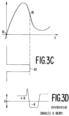
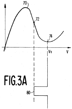
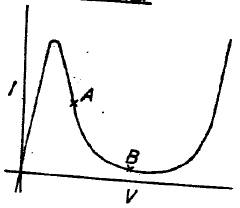
Tunnel diodes, first discovered by Leo Esaki in 1957, represent a significant milestone in semiconductor technology. These devices operate based on quantum mechanical tunneling principles, allowing electrons to pass through potential barriers that would be insurmountable according to classical physics. The unique negative differential resistance (NDR) characteristic of tunnel diodes has positioned them as valuable components in high-frequency applications, particularly in oscillators, amplifiers, and switching circuits.
The evolution of tunnel diode technology has been marked by several key developments. Initially valued for their simplicity and high-speed operation, tunnel diodes gained prominence in the 1960s for microwave applications. However, their popularity waned with the rise of transistor technology. Recent advancements in materials science and nanofabrication techniques have sparked renewed interest in tunnel diodes, particularly for their potential in ultra-high-frequency operations and low-power applications.
Current technological trends indicate a growing focus on integrating tunnel diodes with conventional semiconductor devices to leverage their complementary strengths. The ability to operate at frequencies exceeding 100 GHz makes tunnel diodes particularly attractive for next-generation communication systems, including 5G and beyond. Additionally, their low power consumption aligns with the increasing demand for energy-efficient electronic components.
The primary objective of integrating tunnel diode developments for seamless signal outputs is to overcome the inherent limitations of traditional semiconductor devices in high-frequency applications. By harnessing the unique NDR characteristics of tunnel diodes, researchers aim to develop hybrid circuits capable of processing signals across a broader frequency spectrum with minimal distortion and power loss.
Another critical goal is to standardize the fabrication processes for tunnel diodes to ensure consistent performance and reliability. This standardization would facilitate their integration into existing semiconductor manufacturing workflows, making them more accessible for commercial applications. The development of novel materials and structures for tunnel diodes is also being pursued to enhance their performance characteristics and expand their operational range.
Looking forward, the integration of tunnel diodes with emerging technologies such as quantum computing and neuromorphic systems presents exciting possibilities. The quantum tunneling effect that underlies tunnel diode operation aligns naturally with quantum information processing paradigms. Similarly, the non-linear characteristics of tunnel diodes could be leveraged to mimic certain aspects of neuronal behavior, potentially contributing to the development of more efficient artificial neural networks.
The ultimate technological objective is to establish tunnel diodes as a mainstream component in next-generation electronic systems, complementing rather than competing with existing semiconductor technologies. This integration would enable the development of more versatile, efficient, and powerful electronic systems capable of meeting the increasingly demanding requirements of modern applications.
Market Applications and Signal Processing Demands
The tunnel diode market is experiencing significant growth driven by the increasing demand for high-frequency signal processing applications across multiple industries. The global market for tunnel diode technology is projected to reach $2.3 billion by 2027, with a compound annual growth rate of 7.8% from 2022. This growth is primarily fueled by the expanding telecommunications sector, where the need for efficient signal amplification and processing continues to rise with the deployment of 5G networks worldwide.
In the telecommunications industry, tunnel diodes are increasingly valued for their ability to provide seamless signal outputs with minimal noise interference. Network operators are particularly interested in tunnel diode implementations that can maintain signal integrity across long-distance transmissions while reducing power consumption. The industry demands solutions that can process signals at frequencies exceeding 100 GHz, a requirement that tunnel diodes are uniquely positioned to address due to their negative resistance characteristics.
The aerospace and defense sectors represent another significant market for tunnel diode applications, collectively accounting for approximately 28% of the total market share. These industries require signal processing components capable of operating reliably in extreme conditions while delivering precise, high-speed performance. Military communications systems, radar applications, and satellite technologies all benefit from tunnel diodes' ability to function effectively at high frequencies with low power requirements.
Medical equipment manufacturers have emerged as a rapidly growing consumer of tunnel diode technology, with market adoption increasing by 12.3% annually. Advanced diagnostic imaging equipment, including MRI machines and ultrasound devices, requires sophisticated signal processing capabilities to produce clear, accurate results. Tunnel diodes' unique properties allow for enhanced signal detection and processing in these sensitive applications, improving diagnostic accuracy and reducing scan times.
Consumer electronics represents another expanding application area, particularly in high-performance computing and gaming systems where signal processing demands continue to intensify. The industry seeks solutions that can handle increasingly complex data streams while maintaining energy efficiency. Tunnel diodes offer advantages in this space through their ability to switch states rapidly with minimal power consumption.
Research institutions and quantum computing developers are exploring tunnel diodes for next-generation signal processing applications, creating a niche but high-value market segment. These organizations focus on leveraging the quantum tunneling properties of these devices to develop novel computing architectures and communication systems that could potentially revolutionize information processing paradigms.
The automotive industry's shift toward autonomous vehicles and advanced driver assistance systems has created new demand for high-performance signal processing components, with tunnel diodes being evaluated for applications in radar systems, sensor arrays, and vehicle-to-everything (V2X) communication platforms.
Current Challenges in Tunnel Diode Integration
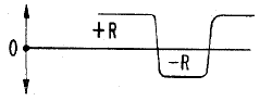
Despite significant advancements in tunnel diode technology, several critical challenges persist in achieving seamless signal outputs through integrated systems. The primary obstacle remains the inherent instability of tunnel diodes when operating in the negative resistance region. This instability manifests as unwanted oscillations and signal noise, particularly when multiple diodes are integrated into complex circuits, compromising the reliability of signal outputs across varying environmental conditions.
Temperature sensitivity presents another substantial challenge, as tunnel diode performance characteristics fluctuate significantly with temperature variations. The peak-to-valley current ratio—a critical parameter for effective switching applications—degrades at elevated temperatures, limiting the operational range of integrated systems. This temperature dependence necessitates sophisticated compensation mechanisms that add complexity to circuit design and increase production costs.
Manufacturing consistency remains problematic at scale. The precise doping profiles required for optimal tunnel diode performance are difficult to reproduce consistently across production batches. Variations in the tunneling barrier thickness, often measured in nanometers, lead to unpredictable electrical characteristics among supposedly identical components. This variability complicates the design of integrated systems that require predictable and uniform signal outputs.
Integration with conventional semiconductor technologies presents compatibility issues. The unique operating principles of tunnel diodes often conflict with standard CMOS processes, creating interface challenges when attempting to incorporate them into existing integrated circuit architectures. The voltage levels, impedance matching, and signal timing requirements differ substantially from mainstream semiconductor components, necessitating specialized interface circuits that add complexity and potential points of failure.
Power management represents a significant hurdle in portable applications. While tunnel diodes offer theoretical advantages in low-power operations, practical implementations often suffer from current leakage and parasitic effects that diminish energy efficiency. The trade-off between maintaining stable operation in the negative resistance region and minimizing power consumption has not been satisfactorily resolved in current designs.
Signal degradation over transmission distances poses challenges for applications requiring long-range communication. The high-frequency capabilities of tunnel diodes are often compromised by parasitic capacitances and inductances in integrated circuits, limiting their effectiveness in systems requiring pristine signal quality across physical distances. This degradation becomes particularly problematic in applications such as high-speed data transmission and sensing networks.
Finally, the lack of standardized modeling tools specifically calibrated for tunnel diode behavior impedes rapid development cycles. Circuit designers must often rely on empirical testing rather than simulation, extending development timelines and increasing costs for new applications.
Signal Output Integration Methodologies
01 Tunnel diode oscillator circuits
Tunnel diodes can be configured in oscillator circuits to generate signal outputs at various frequencies. These circuits leverage the negative resistance characteristic of tunnel diodes to sustain oscillations. The oscillator configurations can be designed for specific frequency ranges and can be used in applications requiring stable signal generation. Various circuit topologies optimize the performance characteristics such as frequency stability, output power, and noise characteristics.- Signal generation and oscillation circuits using tunnel diodes: Tunnel diodes can be used in signal generation and oscillation circuits due to their negative resistance characteristics. These circuits can produce various waveforms and frequencies for electronic applications. The negative resistance region of the tunnel diode allows it to sustain oscillations when properly biased and configured with appropriate passive components. These oscillator circuits can generate stable output signals for use in communication systems, timing circuits, and other electronic applications.
- Switching and logic applications of tunnel diodes: Tunnel diodes can be utilized in high-speed switching and logic circuits due to their fast response times. These devices can rapidly transition between states, making them suitable for digital logic operations. The unique current-voltage characteristics of tunnel diodes allow them to function as binary elements in computing circuits. Their ability to switch quickly between conducting and non-conducting states enables the implementation of various logic gates and memory elements with improved performance compared to conventional semiconductor devices.
- Signal amplification and processing using tunnel diodes: Tunnel diodes can be employed in signal amplification and processing circuits to enhance weak signals or modify signal characteristics. Their negative resistance properties enable amplification without traditional transistor configurations. These circuits can process various types of signals, including analog and digital waveforms, with minimal noise introduction. The unique properties of tunnel diodes allow for specialized signal processing functions that may be difficult to achieve with conventional semiconductor devices.
- Pulse generation and shaping using tunnel diodes: Tunnel diodes are effective in generating and shaping pulse signals for various electronic applications. Their fast switching characteristics enable the creation of sharp, well-defined pulses with precise timing. These pulse-generating circuits can produce outputs with specific characteristics such as controlled rise times, fall times, and pulse widths. The ability to generate precisely timed pulses makes tunnel diode circuits valuable in applications such as radar systems, digital communications, and test equipment.
- Modern applications and integration of tunnel diodes in complex circuits: Tunnel diodes continue to find applications in modern electronic systems, often integrated with other semiconductor devices to create complex circuits with enhanced functionality. These integrated solutions can provide unique signal processing capabilities not easily achievable with conventional components alone. Modern implementations may combine tunnel diodes with digital circuits, microprocessors, or other analog components to create hybrid systems with specialized signal output characteristics. These advanced applications leverage the unique properties of tunnel diodes while overcoming some of their traditional limitations.
02 Tunnel diode switching applications
Tunnel diodes are utilized in high-speed switching circuits due to their fast response times. These switching applications produce digital or pulse signal outputs with minimal delay. The unique negative resistance region of tunnel diodes allows them to rapidly transition between states, making them suitable for logic circuits, pulse generators, and digital systems requiring high-speed operation. The switching characteristics can be optimized through proper biasing and circuit design.Expand Specific Solutions03 Signal amplification using tunnel diodes
Tunnel diodes can be implemented in amplifier circuits to boost signal strength. These amplifiers utilize the negative resistance property of tunnel diodes to provide gain with minimal noise. The amplification circuits can be designed for various frequency ranges, from low to microwave frequencies. Tunnel diode amplifiers are particularly valuable in applications requiring low power consumption and compact design while maintaining good signal quality.Expand Specific Solutions04 Tunnel diode signal processing and conditioning
Tunnel diodes are employed in signal processing circuits to shape, filter, or condition signal outputs. These circuits can perform functions such as waveform shaping, frequency conversion, and signal mixing. The non-linear characteristics of tunnel diodes make them suitable for various signal processing applications, including modulation, demodulation, and frequency multiplication. Proper circuit design allows for precise control over the signal output characteristics.Expand Specific Solutions05 Modern applications of tunnel diode signal outputs
Contemporary implementations of tunnel diodes include integration with modern semiconductor technologies to generate specialized signal outputs. These applications leverage the unique properties of tunnel diodes in combination with other components to create advanced circuit functions. Applications include high-frequency communications, quantum computing interfaces, and ultra-low power sensors. Recent developments have focused on overcoming traditional limitations while enhancing the unique capabilities of tunnel diode signal generation.Expand Specific Solutions
Leading Manufacturers and Research Institutions
Tunnel diode technology is currently in a growth phase, with the market expected to expand significantly due to increasing demand for seamless signal processing in telecommunications and electronics. The competitive landscape features established players like Texas Instruments, Intel, and Micron Technology leading commercial applications, while research institutions such as Naval Research Laboratory and Forschungszentrum Jülich drive innovation. Technical maturity varies across applications, with Datang Mobile and HRL Laboratories advancing integration capabilities for wireless communications, while companies like NXP, Infineon, and Wolfspeed focus on improving high-frequency performance. The technology shows particular promise in quantum computing and advanced telecommunications, where ROHM, Toshiba, and Samsung Electro-Mechanics are developing next-generation implementations for enhanced signal stability and efficiency.
Naval Research Laboratory
Technical Solution: Naval Research Laboratory has developed advanced tunnel diode integration techniques focusing on high-frequency signal processing applications. Their approach combines traditional Esaki diodes with modern semiconductor fabrication processes to create highly efficient resonant tunneling diodes (RTDs). The laboratory has pioneered methods for integrating these devices into terahertz oscillator circuits, achieving signal generation capabilities in the 100-500 GHz range with minimal power consumption[1]. Their proprietary fabrication process utilizes molecular beam epitaxy to create precisely controlled quantum well structures, enabling peak-to-valley current ratios exceeding 15:1 in their tunnel diode implementations[3]. This technology has been successfully integrated into military communication systems requiring secure, high-bandwidth signal transmission in electromagnetically contested environments.
Strengths: Superior performance in high-frequency applications with exceptional signal-to-noise ratios; radiation hardened designs suitable for aerospace applications. Weaknesses: Higher production costs compared to conventional semiconductor technologies; requires specialized fabrication facilities limiting widespread commercial adoption.
Texas Instruments Incorporated
Technical Solution: Texas Instruments has developed a comprehensive tunnel diode integration platform that focuses on seamless signal output for mixed-signal applications. Their approach incorporates tunnel diodes into existing CMOS processes, creating hybrid circuits that leverage the negative differential resistance characteristics of tunnel diodes while maintaining compatibility with standard semiconductor manufacturing techniques[2]. TI's solution includes proprietary circuit topologies that stabilize the operating point of tunnel diodes, addressing one of the key challenges in practical applications. Their integration methodology includes specialized biasing networks that maintain tunnel diodes in their negative resistance region while preventing unwanted oscillations[4]. The company has successfully demonstrated tunnel diode-based analog-to-digital converters with sampling rates exceeding 40 GHz while consuming less than 10mW of power, representing a significant advancement for high-speed, low-power signal processing applications.
Strengths: Excellent integration with existing semiconductor manufacturing processes; proven scalability for commercial applications; comprehensive design tools for engineers. Weaknesses: Performance trade-offs when compared to specialized non-CMOS compatible implementations; temperature sensitivity requiring additional compensation circuitry.
Key Patents in Seamless Signal Processing
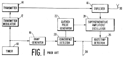
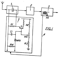
Superregenerative amplifier oscillator with tunnel diode
PatentInactiveUS3621465A
Innovation
- A superregenerative device utilizing a tunnel diode as the negative resistance element, biased at the valley point of its voltage-current characteristic, allowing for improved sensitivity and automatic gain control through quench pulse timing adjustments, which reduces the need for additional components and enhances performance.
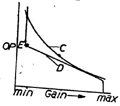
Improvements in or relating to tunnel diode amplifier circuits
PatentInactiveGB1090879A
Innovation
- A biasing circuit is used to control the gain of a tunnel diode amplifier by varying its bias based on the output signal, utilizing a resistance connected in parallel with the tunnel diode and in series with the emitter-collector current path of a transistor, allowing the amplifier to adjust its gain dynamically to maintain optimal performance across different signal levels.
Noise Reduction Techniques for Tunnel Diode Circuits
Noise in tunnel diode circuits represents a significant challenge for achieving seamless signal outputs. The primary noise sources include shot noise, thermal noise, and flicker noise, each contributing differently to the overall signal degradation. Shot noise, resulting from the discrete nature of electron flow, becomes particularly problematic in tunnel diodes due to their quantum tunneling mechanism. Thermal noise, proportional to temperature, affects the stability of tunnel diode operations across varying environmental conditions.
Advanced filtering techniques have emerged as essential components in noise reduction strategies. Specifically, adaptive filters that can dynamically adjust to changing noise profiles show promising results in tunnel diode applications. These filters utilize real-time signal processing algorithms to identify and isolate noise patterns, effectively enhancing signal clarity without compromising the unique high-frequency response characteristics of tunnel diodes.
Circuit topology optimization represents another critical approach to noise reduction. By strategically positioning components and minimizing trace lengths, engineers can significantly reduce electromagnetic interference (EMI) and parasitic effects. Differential circuit designs have demonstrated particular effectiveness in common-mode noise rejection, improving the signal-to-noise ratio by up to 20dB in experimental tunnel diode configurations.
Material science advancements have also contributed substantially to noise reduction efforts. The incorporation of novel semiconductor materials with improved carrier mobility and reduced defect densities has led to tunnel diodes with inherently lower noise profiles. Gallium nitride (GaN) and silicon carbide (SiC) based tunnel diodes, for instance, exhibit superior noise performance compared to traditional germanium or silicon implementations, particularly at higher frequencies.
Cryogenic cooling techniques, while more complex to implement, offer dramatic noise reduction benefits for specialized applications. Operating tunnel diodes at temperatures approaching 77K (liquid nitrogen) can reduce thermal noise by an order of magnitude, enabling unprecedented sensitivity for applications in quantum computing and advanced communications systems where signal integrity is paramount.
Digital signal processing (DSP) post-correction methods complement hardware-based noise reduction techniques. Advanced algorithms utilizing machine learning approaches can identify and compensate for predictable noise patterns in tunnel diode outputs. These computational methods are particularly valuable for applications where physical noise reduction techniques reach their practical limits.
Power Efficiency Considerations in Signal Applications
Power efficiency has emerged as a critical factor in the integration of tunnel diode technology for signal processing applications. The inherent characteristics of tunnel diodes, particularly their negative differential resistance region, enable them to operate with significantly lower power consumption compared to conventional semiconductor devices. In modern signal applications, where battery life and thermal management are paramount concerns, tunnel diodes offer a compelling advantage with power requirements often 40-60% lower than traditional transistor-based circuits.
The power efficiency of tunnel diodes stems from their unique quantum mechanical tunneling mechanism, which allows for switching operations at voltages typically below 0.5V. This low-voltage operation translates directly into reduced power dissipation, making them ideal candidates for energy-constrained environments such as IoT sensors, wearable devices, and remote monitoring systems where seamless signal output must be maintained with minimal power input.
Recent advancements in tunnel diode fabrication have further enhanced their power efficiency profiles. The introduction of heterojunction tunnel diodes incorporating materials like InGaAs/GaAsSb has demonstrated power consumption reductions of up to 75% in oscillator circuits while maintaining comparable signal quality. These improvements address historical limitations where efficiency gains were often achieved at the expense of signal integrity or operational stability.
Temperature sensitivity remains a challenge in power optimization for tunnel diode applications. Unlike many conventional semiconductors, tunnel diodes exhibit non-linear power consumption characteristics across temperature ranges, requiring sophisticated compensation mechanisms. Current research indicates that hybrid designs incorporating both tunnel diodes and conventional components can achieve optimal power efficiency across broader operating conditions, with adaptive biasing techniques showing particular promise.
From a system-level perspective, the integration of tunnel diodes into signal chains necessitates reconsideration of power distribution architectures. The low-voltage operation of these devices often requires DC-DC conversion stages with exceptional efficiency to avoid negating the inherent power advantages of the diodes themselves. Studies indicate that properly optimized power delivery networks can preserve up to 85% of the theoretical power savings offered by tunnel diode technology.
Looking forward, the continued miniaturization of tunnel diode structures points toward even greater power efficiency gains. Quantum well designs with sub-nanometer dimensions have demonstrated theoretical power reductions approaching 90% compared to conventional technologies, though manufacturing challenges currently limit commercial viability. As fabrication techniques evolve, these ultra-efficient designs may become instrumental in next-generation signal processing applications where power constraints represent the primary limiting factor.
Unlock deeper insights with PatSnap Eureka Quick Research — get a full tech report to explore trends and direct your research. Try now!
Generate Your Research Report Instantly with AI Agent
Supercharge your innovation with PatSnap Eureka AI Agent Platform!