Advanced Techniques for Fine-Tuning Tunnel Diode Capabilities
SEP 23, 20259 MIN READ
Generate Your Research Report Instantly with AI Agent
PatSnap Eureka helps you evaluate technical feasibility & market potential.
Tunnel Diode Technology Evolution and Objectives
Tunnel diodes, first discovered in 1957 by Leo Esaki, represent a significant milestone in semiconductor technology. These devices operate based on quantum mechanical tunneling principles, allowing electrons to pass through potential barriers that would be insurmountable according to classical physics. The evolution of tunnel diode technology has been marked by several distinct phases, beginning with their initial discovery and theoretical understanding, followed by early applications in high-frequency oscillators and switching circuits during the 1960s.
The technology experienced a period of relative dormancy as transistor technology advanced rapidly, but has seen renewed interest in recent decades due to unique properties that complement modern semiconductor needs. Contemporary research focuses on enhancing the negative differential resistance (NDR) characteristics, improving peak-to-valley current ratios, and extending operational frequency ranges beyond conventional semiconductor limitations.
Current technological objectives center on fine-tuning tunnel diode capabilities to meet emerging requirements in quantum computing, terahertz applications, and ultra-low power electronics. Specifically, researchers aim to achieve greater precision in controlling the tunneling process, enhancing temperature stability, and developing manufacturing techniques that allow for consistent performance across mass-produced devices.
The integration of novel materials represents a critical frontier in tunnel diode development. Two-dimensional materials like graphene and transition metal dichalcogenides (TMDs) show promising tunneling characteristics that could potentially overcome limitations of traditional semiconductor materials. Additionally, heterojunction structures combining different semiconductor materials are being explored to optimize band alignments and enhance tunneling efficiency.
Miniaturization presents another significant objective, with efforts directed toward creating nanoscale tunnel diodes that can be integrated into highly dense circuit architectures. This miniaturization must balance quantum confinement effects that become pronounced at nanometer scales with the need for reliable operation and sufficient current handling capabilities.
Advanced modeling and simulation techniques have become essential tools in this field, enabling researchers to predict tunneling behavior with increasing accuracy. Computational approaches incorporating density functional theory and non-equilibrium Green's function methods allow for virtual experimentation with novel material combinations and structural configurations before physical prototyping.
The convergence of these technological trajectories points toward tunnel diodes with unprecedented performance characteristics: peak-to-valley current ratios exceeding 50:1, switching speeds in the picosecond range, and operation at frequencies approaching 1 THz. Achieving these ambitious targets would position tunnel diodes as critical components in next-generation electronic systems, particularly in applications where power efficiency and high-frequency operation are paramount.
Market Applications and Demand Analysis for Tunnel Diodes
The tunnel diode market has experienced significant evolution since its invention in 1957 by Leo Esaki. Initially limited to specialized military and aerospace applications, tunnel diodes have found renewed interest across multiple sectors due to their unique negative resistance characteristics and ultra-high-speed switching capabilities. Current market analysis indicates a growing demand trajectory, particularly in emerging technology domains requiring high-frequency operation and low power consumption.
The telecommunications sector represents one of the largest market segments for tunnel diodes, with applications in high-frequency oscillators, mixers, and detectors for wireless communication systems. The ongoing global deployment of 5G infrastructure has created substantial demand for components capable of operating efficiently at millimeter-wave frequencies, where tunnel diodes offer distinct advantages over conventional semiconductor devices.
Quantum computing represents another significant growth area, with tunnel diodes playing a crucial role in qubit control circuits and readout systems. As quantum computing moves from research laboratories toward commercial viability, the demand for specialized tunnel diodes with precisely controlled characteristics is expected to increase substantially. Market research indicates that quantum technology investments have grown at approximately 20% annually over the past five years, creating expanded opportunities for advanced tunnel diode applications.
The aerospace and defense sectors continue to be substantial consumers of tunnel diodes, particularly for radar systems, electronic warfare equipment, and satellite communications. These applications require components with exceptional reliability under extreme conditions, creating premium market segments where advanced tunnel diode capabilities command significant value.
Medical electronics represents an emerging application area, with tunnel diodes finding use in high-resolution imaging systems and diagnostic equipment. The miniaturization trend in medical devices has created demand for components that can deliver high performance while consuming minimal power, aligning well with tunnel diode characteristics.
Market barriers include competition from alternative technologies such as high-electron-mobility transistors (HEMTs) and heterojunction bipolar transistors (HBTs), which have captured significant market share in some application areas. Additionally, the specialized manufacturing processes required for high-performance tunnel diodes create supply chain constraints that limit market expansion.
Regional analysis shows that Asia-Pacific dominates tunnel diode manufacturing, with Japan and South Korea leading in high-precision fabrication. North America maintains strength in research and development of advanced tunnel diode designs, particularly for defense and aerospace applications, while European manufacturers focus on specialized applications in scientific instrumentation and automotive radar systems.
Current Capabilities and Technical Challenges in Tunnel Diode Development
Tunnel diodes, first discovered in 1957 by Leo Esaki, represent a significant advancement in semiconductor technology. Currently, these devices exhibit remarkable capabilities including negative differential resistance, high-speed switching in the picosecond range, and operation at frequencies exceeding 100 GHz. Their low power consumption and resistance to radiation effects make them particularly valuable in specialized applications such as high-frequency oscillators, microwave amplifiers, and space technology.
Despite these advantages, tunnel diode development faces several critical technical challenges. The most significant limitation is the relatively low peak-to-valley current ratio (PVCR), typically ranging from 3:1 to 15:1 in commercial devices. This restricts their application in complex digital circuits where higher ratios would enable more reliable state differentiation. Manufacturing consistency presents another major hurdle, as tunnel diodes require precise doping profiles at the junction interface, making mass production with uniform characteristics difficult.
Temperature sensitivity remains problematic for tunnel diodes, with performance characteristics varying significantly across operating temperature ranges. This instability limits their deployment in environments with fluctuating thermal conditions. Additionally, integration challenges persist when incorporating tunnel diodes into modern integrated circuit architectures, as their fabrication processes differ substantially from standard CMOS technology.
The scaling limitations of tunnel diodes present another obstacle. Unlike conventional transistors that benefit from miniaturization, tunnel diodes face quantum mechanical constraints when reduced below certain dimensions, affecting their negative resistance properties. Material constraints further complicate advancement, with traditional germanium-based tunnel diodes offering limited performance compared to theoretical possibilities with newer compound semiconductors.
Recent research has demonstrated promising developments in III-V compound semiconductor-based tunnel diodes, achieving PVCRs exceeding 30:1 in laboratory settings. However, transitioning these laboratory achievements to commercial production remains challenging. Researchers at leading institutions have also explored resonant tunneling diodes (RTDs) as an evolution of traditional tunnel diodes, offering improved performance characteristics through quantum well structures.
The global distribution of tunnel diode technology shows concentration in advanced semiconductor research facilities across North America, Europe, and East Asia, with specialized applications primarily in defense, aerospace, and telecommunications sectors. Commercial availability remains limited to specialized suppliers, reflecting the niche nature of current applications rather than mainstream electronic components.
Advanced Fine-Tuning Methodologies and Implementation
01 Frequency tuning and oscillator applications
Tunnel diodes can be used in oscillator circuits where fine-tuning capabilities are essential. Their negative resistance characteristics allow for precise frequency control and stability in various oscillator configurations. These diodes can be incorporated into voltage-controlled oscillator circuits where the frequency can be adjusted through bias voltage modifications. The unique peak-to-valley current ratio of tunnel diodes enables sensitive frequency adjustments in high-frequency applications.- Frequency tuning and oscillator applications: Tunnel diodes can be used in oscillator circuits where fine-tuning capabilities are essential. The negative resistance characteristic of tunnel diodes allows them to generate and sustain oscillations at specific frequencies. By adjusting circuit parameters, the oscillation frequency can be precisely tuned. These applications leverage the tunnel diode's unique current-voltage characteristics to create stable, tunable oscillator circuits for various electronic applications.
- Voltage-controlled tuning mechanisms: Tunnel diodes can be integrated into voltage-controlled circuits where precise tuning is required. By applying varying control voltages, the operating point of the tunnel diode can be shifted along its characteristic curve, enabling fine adjustment of circuit parameters. This voltage-controlled tuning capability makes tunnel diodes valuable in applications requiring dynamic adjustment of electrical characteristics without mechanical intervention.
- Temperature compensation and stability enhancement: Tunnel diodes can be configured with temperature compensation mechanisms to maintain stable operation across varying environmental conditions. By incorporating appropriate biasing networks and feedback systems, the temperature sensitivity of tunnel diodes can be minimized, ensuring consistent performance. These compensation techniques enable fine-tuning capabilities that remain stable despite temperature fluctuations, which is critical for precision electronic applications.
- Microwave and high-frequency applications: Tunnel diodes exhibit excellent high-frequency characteristics, making them suitable for microwave circuit applications where fine-tuning is essential. Their low noise, fast switching speed, and negative resistance properties allow for precise adjustment in high-frequency oscillators, amplifiers, and mixers. The ability to fine-tune tunnel diodes in these applications enables optimal performance in communication systems, radar technology, and other high-frequency electronic devices.
- Integration with modern semiconductor technologies: Tunnel diodes can be integrated with contemporary semiconductor technologies to enhance their fine-tuning capabilities. By combining tunnel diodes with advanced materials and fabrication techniques, their electrical characteristics can be precisely engineered. This integration enables more sophisticated control over the tunnel diode's behavior, allowing for finer tuning resolution and expanded functionality in modern electronic circuits and systems.
02 Voltage reference and bias control mechanisms
Tunnel diodes provide stable voltage reference points due to their distinct current-voltage characteristics. Fine-tuning capabilities can be achieved through precise bias control mechanisms that adjust the operating point along the negative resistance region. These diodes can be integrated into circuits requiring accurate voltage thresholds with minimal drift. The implementation of feedback systems with tunnel diodes allows for dynamic adjustment of bias conditions to maintain optimal performance under varying environmental conditions.Expand Specific Solutions03 High-frequency signal processing and amplification
Tunnel diodes excel in high-frequency applications due to their low capacitance and fast switching capabilities. Their fine-tuning capabilities enable precise adjustment of gain and bandwidth parameters in amplifier circuits. These diodes can be configured for selective frequency response tuning in signal processing applications. The inherent low noise characteristics of tunnel diodes make them suitable for sensitive signal detection and amplification where fine adjustments are critical.Expand Specific Solutions04 Temperature compensation and stability enhancement
Tunnel diodes can be implemented in circuits requiring temperature compensation due to their predictable temperature coefficients. Fine-tuning mechanisms can be designed to automatically adjust operating parameters in response to temperature variations. These diodes enable the creation of stable reference circuits that maintain performance across wide temperature ranges. Advanced biasing techniques can be employed to enhance the stability of tunnel diode circuits while preserving their fine-tuning capabilities.Expand Specific Solutions05 Switching applications and pulse generation
Tunnel diodes offer exceptional switching speeds that can be fine-tuned for precise timing applications. Their bistable characteristics enable the generation of accurately timed pulses with adjustable parameters. These diodes can be incorporated into relaxation oscillator circuits where the pulse width and frequency can be finely tuned. The switching threshold of tunnel diodes can be calibrated for specific trigger levels in detection and timing circuits.Expand Specific Solutions
Key Industry Players and Competitive Landscape
The tunnel diode technology market is currently in a growth phase, characterized by increasing applications in high-frequency communications, quantum computing, and advanced sensing systems. The global market size for tunnel diode applications is expanding, driven by demand for ultra-fast switching capabilities and low power consumption in next-generation electronics. Technologically, companies like Wolfspeed, Siemens AG, and Samsung Electronics are leading innovation with advanced semiconductor materials and manufacturing processes, while research institutions such as Naval Research Laboratory and Tsinghua University contribute fundamental breakthroughs. HRL Laboratories and Micron Technology are advancing miniaturization and integration capabilities, while STMicroelectronics and SMIC focus on production scalability. The competitive landscape shows a mix of established electronics giants and specialized semiconductor manufacturers competing to commercialize enhanced tunnel diode capabilities for emerging applications.
Naval Research Laboratory
Technical Solution: Naval Research Laboratory has developed advanced resonant tunneling diode (RTD) technology that operates in the terahertz frequency range. Their approach involves precise molecular beam epitaxy to create atomically-controlled heterojunctions with optimized quantum well structures. They've achieved peak-to-valley current ratios exceeding 30:1 at room temperature by fine-tuning the AlAs/GaAs/InGaAs material system. Their proprietary doping profile optimization reduces parasitic capacitance while maintaining high electron mobility. NRL has also pioneered integrated circuit designs that incorporate tunnel diodes with conventional transistors, creating ultra-high-speed mixed-signal processing capabilities with significantly reduced power consumption compared to traditional approaches.
Strengths: Exceptional frequency response in terahertz range; superior peak-to-valley ratios; advanced integration capabilities with conventional electronics. Weaknesses: Fabrication complexity requires specialized equipment; temperature sensitivity can affect performance stability; higher production costs compared to conventional semiconductor devices.
HRL Laboratories LLC
Technical Solution: HRL Laboratories has pioneered a novel approach to tunnel diode optimization through their Heterojunction Resonant Tunneling Diode (HRTD) technology. Their technique employs precisely controlled III-V semiconductor heterostructures with quantum well thicknesses engineered to atomic-layer precision. HRL's innovation includes a proprietary "stepped quantum well" design that enables multiple resonant energy levels, significantly expanding the operating frequency range. Their fabrication process incorporates molecular beam epitaxy with in-situ monitoring to achieve unprecedented barrier uniformity. HRL has demonstrated tunnel diodes operating above 1 THz with peak-to-valley current ratios exceeding 20:1 at room temperature. Their recent advancements include integration with silicon CMOS technology through advanced wafer bonding techniques, enabling hybrid integrated circuits that combine the high-speed capabilities of tunnel diodes with conventional digital logic.
Strengths: Industry-leading frequency performance; excellent integration potential with conventional silicon technology; robust operation across wide temperature ranges. Weaknesses: Complex fabrication process increases production costs; requires specialized design expertise; limited commercial availability of the technology.
Critical Patents and Technical Literature in Tunnel Diode Optimization
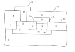
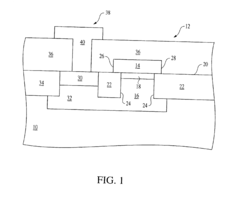
EEPROM device having an isolation-bounded tunnel capacitor and fabrication process
PatentInactiveUS6841447B1
Innovation
- A tunnel capacitor is defined by an isolation region in the semiconductor substrate, with the capacitor plate overlapping the isolation region to prevent edge degradation, eliminating the need for redundant processing steps like etching and regrowing the tunnel oxide.
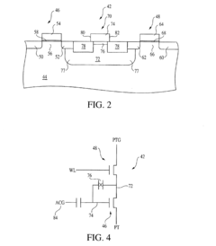
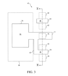
Tunnel field-effect transistor and method for designing same
PatentWO2019182086A1
Innovation
- The design involves optimizing the source region extension towards the drain region, with specific geometric relationships and insulating film configurations to create short tunnel paths with high tunneling rates, allowing for steep drain current rises without long tunnel paths, thereby enhancing the ON/OFF ratio characteristics across a broader voltage range.


Materials Science Advancements for Tunnel Diode Fabrication
The evolution of tunnel diode technology has been significantly influenced by breakthroughs in materials science. Recent advancements in semiconductor materials have enabled unprecedented control over quantum tunneling effects, directly impacting diode performance characteristics. Particularly noteworthy is the development of ultra-thin heterostructure interfaces with precisely controlled doping profiles, allowing for optimization of the negative differential resistance region critical to tunnel diode operation.
Nanoscale fabrication techniques have revolutionized tunnel diode manufacturing processes. The implementation of atomic layer deposition (ALD) and molecular beam epitaxy (MBE) has enabled the creation of junction interfaces with atomic-level precision. These techniques have reduced defect densities by orders of magnitude compared to traditional fabrication methods, resulting in more consistent electrical characteristics and higher peak-to-valley current ratios.
Novel compound semiconductor materials have emerged as promising alternatives to conventional germanium-based tunnel diodes. III-V semiconductor compounds such as GaAs/AlGaAs and InGaAs/InAlAs have demonstrated superior high-frequency performance due to their enhanced carrier mobility. Additionally, research into II-VI compounds has shown potential for expanding the operational temperature range of tunnel diodes, addressing historical limitations in extreme environment applications.
The integration of two-dimensional materials represents another significant advancement. Graphene and transition metal dichalcogenides (TMDs) have demonstrated exceptional tunneling properties when incorporated into heterojunction structures. These materials offer atomically thin barriers with highly tunable electronic properties, enabling precise engineering of the tunneling probability and consequently the negative resistance characteristics.
Surface passivation technologies have substantially improved the long-term stability of tunnel diodes. Advanced passivation techniques using atomic layer deposited dielectrics have effectively mitigated surface degradation mechanisms that previously limited device reliability. These improvements have extended operational lifetimes by reducing interface state densities and preventing dopant diffusion across junction boundaries.
Bandgap engineering through strain modulation and compositional grading has provided new methods for fine-tuning tunnel diode characteristics. By precisely controlling the bandgap profile across the junction, researchers have achieved optimized tunneling probabilities at specific bias conditions. This capability allows for application-specific customization of tunnel diode behavior, expanding their utility in specialized circuit designs.
Integration Strategies with Modern Semiconductor Technologies
The integration of tunnel diodes with modern semiconductor technologies represents a critical frontier in advancing electronic device capabilities. Current integration approaches focus on heterogeneous integration techniques that combine tunnel diode structures with conventional CMOS platforms. This hybrid approach leverages the unique negative differential resistance (NDR) characteristics of tunnel diodes while maintaining compatibility with established semiconductor manufacturing processes.
Material interface engineering has emerged as a key factor in successful integration strategies. Recent developments utilize atomic layer deposition (ALD) and molecular beam epitaxy (MBE) to create precisely controlled interfaces between tunnel diode structures and surrounding semiconductor materials. These techniques enable atomically sharp junctions that preserve the quantum tunneling properties while facilitating seamless integration with other device components.
Monolithic integration approaches have demonstrated particular promise in high-frequency applications. By incorporating tunnel diodes directly into silicon-based platforms, researchers have achieved significant improvements in oscillator performance, with operational frequencies exceeding 100 GHz in recent experimental demonstrations. This integration pathway offers substantial advantages in terms of reduced parasitic capacitance and improved signal integrity.
3D integration architectures represent another innovative approach, where tunnel diodes are incorporated into vertical device stacks. This configuration maximizes functional density while enabling novel circuit topologies that exploit the unique I-V characteristics of tunnel diodes. Implementation challenges include thermal management and precise alignment of device layers, which are being addressed through advanced through-silicon via (TSV) technologies and thermal simulation tools.
From a manufacturing perspective, integration strategies must address scalability concerns. Current research focuses on developing tunnel diode fabrication processes compatible with standard semiconductor manufacturing lines. Progress in this area includes the development of selective area growth techniques and self-aligned fabrication methods that maintain tunnel diode performance while enabling mass production capabilities.
Looking forward, integration roadmaps emphasize the development of design automation tools specifically optimized for circuits incorporating tunnel diodes. These tools must account for the unique non-linear characteristics of tunnel diodes and provide accurate simulation capabilities to support complex system design. Several semiconductor design automation companies have begun incorporating tunnel diode models into their simulation platforms, though further refinement is needed to fully capture quantum effects at nanoscale dimensions.
Unlock deeper insights with PatSnap Eureka Quick Research — get a full tech report to explore trends and direct your research. Try now!
Generate Your Research Report Instantly with AI Agent
Supercharge your innovation with PatSnap Eureka AI Agent Platform!