How to Boost Tunnel Diode Efficiency in Power Converters
SEP 23, 202510 MIN READ
Generate Your Research Report Instantly with AI Agent
Patsnap Eureka helps you evaluate technical feasibility & market potential.
Tunnel Diode Technology Evolution and Objectives
Tunnel diodes, first discovered in 1957 by Leo Esaki, represent a significant milestone in semiconductor technology. These devices operate based on quantum mechanical tunneling principles, allowing electrons to pass through potential barriers rather than overcoming them. The evolution of tunnel diodes has been marked by several key developments, from their initial discovery to their integration into modern power conversion systems.
In the 1960s, tunnel diodes were primarily used in high-frequency oscillators and amplifiers due to their negative differential resistance characteristics. However, their application in power conversion remained limited due to efficiency constraints and manufacturing challenges. The 1970s and 1980s witnessed gradual improvements in fabrication techniques, enabling better control over the tunneling barrier width and doping profiles, which are critical parameters affecting efficiency.
The 1990s marked a turning point with the emergence of resonant tunneling diodes (RTDs), offering enhanced control over electron transport. This period also saw the development of interband tunneling diodes, which exploit band-to-band tunneling mechanisms to achieve higher current densities. These advancements laid the groundwork for exploring tunnel diodes in power conversion applications, though efficiency remained a significant challenge.
The early 2000s brought renewed interest in tunnel diodes for power applications, driven by the increasing demand for high-efficiency, compact power converters in portable electronics and telecommunications. Research focused on optimizing the tunneling barrier properties and reducing parasitic resistances to improve efficiency. Concurrently, advances in materials science enabled the exploration of novel semiconductor compounds with superior tunneling characteristics.
Recent technological trends have centered on enhancing tunnel diode efficiency through nanoscale engineering and heterojunction designs. The integration of tunnel diodes with wide-bandgap semiconductors like GaN and SiC has shown promising results for high-power applications. Additionally, the development of tunnel field-effect transistors (TFETs) has opened new avenues for tunnel-based power conversion with reduced switching losses.
The primary objective in tunnel diode research for power converters is to overcome the efficiency limitations while maintaining their inherent advantages of fast switching speeds and negative differential resistance. Specific goals include increasing the peak-to-valley current ratio, reducing the valley current, and enhancing thermal stability. These improvements are essential for tunnel diodes to compete with conventional power semiconductor devices in terms of efficiency and reliability.
Looking forward, the field aims to develop tunnel diodes capable of operating at higher voltages and currents while maintaining high efficiency across a wide temperature range. This requires interdisciplinary approaches combining semiconductor physics, materials science, and circuit design to optimize the overall system performance rather than focusing solely on device-level improvements.
Market Analysis for High-Efficiency Power Converters
The global market for high-efficiency power converters has experienced substantial growth in recent years, driven primarily by increasing demand for energy-efficient solutions across multiple industries. The power converter market reached approximately $29.3 billion in 2022 and is projected to grow at a compound annual growth rate (CAGR) of 6.8% through 2028, potentially reaching $43.7 billion by the end of the forecast period.
Tunnel diode-based power converters represent a specialized segment within this broader market, currently accounting for a relatively small but growing share. Their unique negative resistance characteristics make them particularly valuable in high-frequency applications where conventional diodes face efficiency limitations.
Key market drivers for high-efficiency power converters include the rapid expansion of renewable energy systems, which require advanced power conversion technologies to maximize energy harvest. The electric vehicle (EV) market has emerged as another significant demand center, with manufacturers seeking increasingly efficient power conversion solutions to extend vehicle range and reduce charging times.
Data center infrastructure represents another substantial market opportunity, with the global shift toward cloud computing creating unprecedented demand for energy-efficient power conversion systems. According to industry reports, data centers currently consume approximately 1-2% of global electricity, with power conversion losses accounting for 10-15% of this consumption.
Regional analysis reveals that Asia-Pacific dominates the high-efficiency power converter market, accounting for approximately 42% of global demand. This is largely attributed to the region's robust electronics manufacturing ecosystem and aggressive renewable energy deployment. North America and Europe follow with market shares of approximately 28% and 23% respectively.
Consumer electronics continues to be the largest application segment, representing approximately 35% of the total market value. However, industrial applications and automotive sectors are showing the fastest growth rates at 8.2% and 9.5% respectively.
The market landscape for tunnel diode technology specifically shows promising growth potential but faces competition from alternative technologies such as silicon carbide (SiC) and gallium nitride (GaN) power devices. These competing technologies currently hold larger market shares due to their established manufacturing infrastructure and wider commercial availability.
End-user surveys indicate increasing awareness of power conversion efficiency as a critical factor in purchasing decisions, with 78% of industrial customers citing energy efficiency as a "very important" consideration. This trend is particularly pronounced in regions with high electricity costs or stringent energy efficiency regulations.
Current Limitations in Tunnel Diode Implementation
Despite the promising theoretical advantages of tunnel diodes in power conversion applications, several significant limitations currently hinder their widespread implementation and efficiency optimization. The primary challenge lies in the inherently narrow negative differential resistance (NDR) region, which restricts the operational voltage range to typically less than 500mV. This narrow operating window severely constrains power handling capabilities, making tunnel diodes less suitable for high-power applications compared to conventional semiconductor devices.
Material constraints represent another major limitation. Traditional tunnel diodes fabricated from germanium or gallium arsenide exhibit suboptimal performance characteristics, including limited peak-to-valley current ratios (PVCR) typically ranging from 3:1 to 8:1. These modest ratios directly impact switching efficiency and contribute to significant power losses during operation, particularly at higher frequencies where parasitic effects become more pronounced.
Temperature sensitivity poses a substantial challenge for practical implementations. Tunnel diodes demonstrate marked performance degradation as operating temperatures increase, with the NDR region characteristics deteriorating significantly above 85°C. This thermal instability necessitates complex cooling solutions in power converter designs, adding cost, weight, and reliability concerns to the overall system architecture.
Manufacturing consistency remains problematic for tunnel diode production. Current fabrication techniques struggle to achieve uniform doping profiles at the extremely high concentrations (>10^19 cm^-3) required for optimal tunneling effects. This variability leads to inconsistent device characteristics even within the same production batch, complicating circuit design and reducing overall system reliability in power conversion applications.
Integration challenges with conventional power electronics further limit implementation. Tunnel diodes typically require specialized biasing circuits and protection mechanisms that add complexity to the overall system design. The lack of standardized packaging and interface solutions compatible with modern power electronic modules creates additional barriers to adoption in commercial power converter applications.
Scaling limitations represent a significant obstacle to higher power applications. Unlike traditional semiconductor devices that benefit from parallel configuration for increased current handling, tunnel diodes exhibit complex behavior when connected in parallel due to their unique I-V characteristics. This fundamentally restricts their application in higher power density converters where current requirements exceed the capabilities of individual devices.
Finally, the economic viability of tunnel diode implementation remains questionable. Current manufacturing costs significantly exceed those of conventional power semiconductor devices, while performance advantages in most applications remain marginal or application-specific. This unfavorable cost-benefit ratio has limited research investment and technological advancement in tunnel diode optimization for power conversion applications.
Existing Efficiency Enhancement Techniques
01 Efficiency improvements in tunnel diode design
Various design modifications can enhance the efficiency of tunnel diodes. These include optimizing the doping profile, improving the junction interface quality, and reducing parasitic resistances. Such improvements allow for better energy conversion and reduced power losses during operation, making tunnel diodes more efficient for electronic applications.- Efficiency improvements in tunnel diode design: Various design modifications can enhance the efficiency of tunnel diodes. These include optimizing the doping profile, improving the junction structure, and refining the semiconductor materials used. Such improvements lead to better peak-to-valley current ratios, reduced power losses, and overall higher operational efficiency in tunnel diode applications.
- Tunnel diodes in energy harvesting applications: Tunnel diodes demonstrate significant efficiency advantages in energy harvesting systems due to their ability to operate at low voltage thresholds. Their negative resistance characteristics enable effective conversion of small energy inputs into usable power, making them particularly valuable in renewable energy systems, waste heat recovery, and self-powered electronic devices.
- High-frequency performance optimization: Tunnel diodes can achieve exceptional efficiency in high-frequency applications through specialized design considerations. By minimizing parasitic capacitance and inductance, optimizing the junction area, and employing advanced fabrication techniques, these diodes can operate efficiently at microwave and millimeter-wave frequencies with reduced switching losses and improved signal integrity.
- Thermal management for efficiency enhancement: Effective thermal management significantly impacts tunnel diode efficiency. Techniques such as heat sinking, substrate material selection, and package design can reduce operating temperature and prevent performance degradation. Lower operating temperatures maintain optimal tunneling conditions, preserve the negative resistance characteristics, and extend device lifetime while ensuring consistent efficiency.
- Circuit integration techniques for optimal efficiency: Specialized circuit integration approaches can maximize tunnel diode efficiency in practical applications. These include impedance matching networks, bias stabilization circuits, and complementary component selection. Proper integration ensures that the unique negative resistance properties of tunnel diodes are fully utilized while minimizing losses at interfaces with other circuit elements, resulting in higher system-level efficiency.
02 Tunnel diode oscillator efficiency
Tunnel diodes can be configured as efficient oscillators due to their negative resistance characteristics. By optimizing the circuit configuration and operating parameters, tunnel diode oscillators can achieve higher efficiency in frequency generation and conversion applications. These oscillators are particularly useful in high-frequency applications where energy efficiency is critical.Expand Specific Solutions03 Thermal efficiency and heat management in tunnel diodes
Managing thermal effects is crucial for maintaining tunnel diode efficiency. Techniques include improved heat dissipation designs, temperature compensation circuits, and materials with better thermal conductivity. These approaches help maintain stable operation across temperature variations and prevent efficiency degradation due to thermal effects.Expand Specific Solutions04 Integration of tunnel diodes in energy harvesting systems
Tunnel diodes can be effectively integrated into energy harvesting systems to improve overall efficiency. Their unique current-voltage characteristics make them suitable for converting small voltage differentials into usable power. Applications include thermal energy harvesting, electromagnetic energy conversion, and low-power electronic systems where efficiency in energy capture and conversion is paramount.Expand Specific Solutions05 Novel materials and fabrication techniques for high-efficiency tunnel diodes
Advanced materials and fabrication methods can significantly enhance tunnel diode efficiency. These include using compound semiconductors, nanoscale fabrication techniques, and novel junction materials. Such innovations lead to improved carrier tunneling probability, reduced leakage currents, and enhanced overall energy conversion efficiency in tunnel diode applications.Expand Specific Solutions
Leading Manufacturers and Research Institutions
The tunnel diode power converter market is currently in a growth phase, with increasing demand for high-efficiency power conversion solutions driving innovation. The market size is expanding as energy efficiency becomes paramount across industries, particularly in telecommunications and renewable energy sectors. Technologically, tunnel diodes in power converters are approaching maturity, with companies like Huawei Technologies and Infineon Technologies leading development through significant R&D investments. Siemens, Texas Instruments, and Mitsubishi Electric have established strong positions by integrating tunnel diode technology into their power management portfolios. Research institutions like Forschungszentrum Jülich and HRL Laboratories are advancing fundamental breakthroughs, while Qualcomm and Renesas Electronics focus on miniaturization for mobile applications. The competitive landscape shows a balance between established electronics giants and specialized semiconductor manufacturers working to overcome efficiency limitations.
Huawei Technologies Co., Ltd.
Technical Solution: Huawei has pioneered an advanced tunnel diode implementation for telecommunications power systems that focuses on miniaturization and efficiency. Their approach combines III-V semiconductor materials with proprietary doping techniques to create tunnel diodes with peak-to-valley current ratios exceeding 15:1. This technology has been integrated into their distributed power architecture, where multiple small tunnel diode converters operate in parallel, achieving system efficiency improvements of approximately 22% over traditional designs. Huawei's solution incorporates adaptive biasing circuits that dynamically adjust the operating point of each tunnel diode to maintain operation in the negative resistance region despite temperature and load variations. The company has also developed specialized thermal management solutions that allow their tunnel diode converters to operate reliably in compact telecommunications equipment.
Strengths: Exceptional power density suitable for space-constrained applications; highly efficient at partial loads; excellent integration with digital control systems. Weaknesses: Complex manufacturing process increases production costs; requires sophisticated control algorithms; limited applicability in very high power applications.
ABB Group
Technical Solution: ABB has developed a comprehensive tunnel diode solution for industrial power conversion applications that focuses on reliability and efficiency. Their approach utilizes germanium-based tunnel diodes with specialized epitaxial growth techniques to achieve peak current densities exceeding 100kA/cm². ABB's implementation incorporates resonant tank circuits that leverage the negative differential resistance properties of tunnel diodes to achieve zero-voltage switching, reducing conversion losses by approximately 28% compared to conventional topologies. The company has also pioneered advanced thermal management techniques specifically designed for tunnel diode applications, including direct liquid cooling interfaces that maintain optimal junction temperatures under high-power operation. ABB's solution includes proprietary control algorithms that compensate for the non-linear characteristics of tunnel diodes, ensuring stable operation across varying input voltages and load conditions.
Strengths: Exceptional reliability in harsh industrial environments; superior efficiency at high power levels; excellent thermal performance under continuous operation. Weaknesses: Higher initial cost compared to conventional solutions; requires specialized design expertise; limited flexibility for rapid design iterations.
Critical Patents in Tunnel Diode Technology
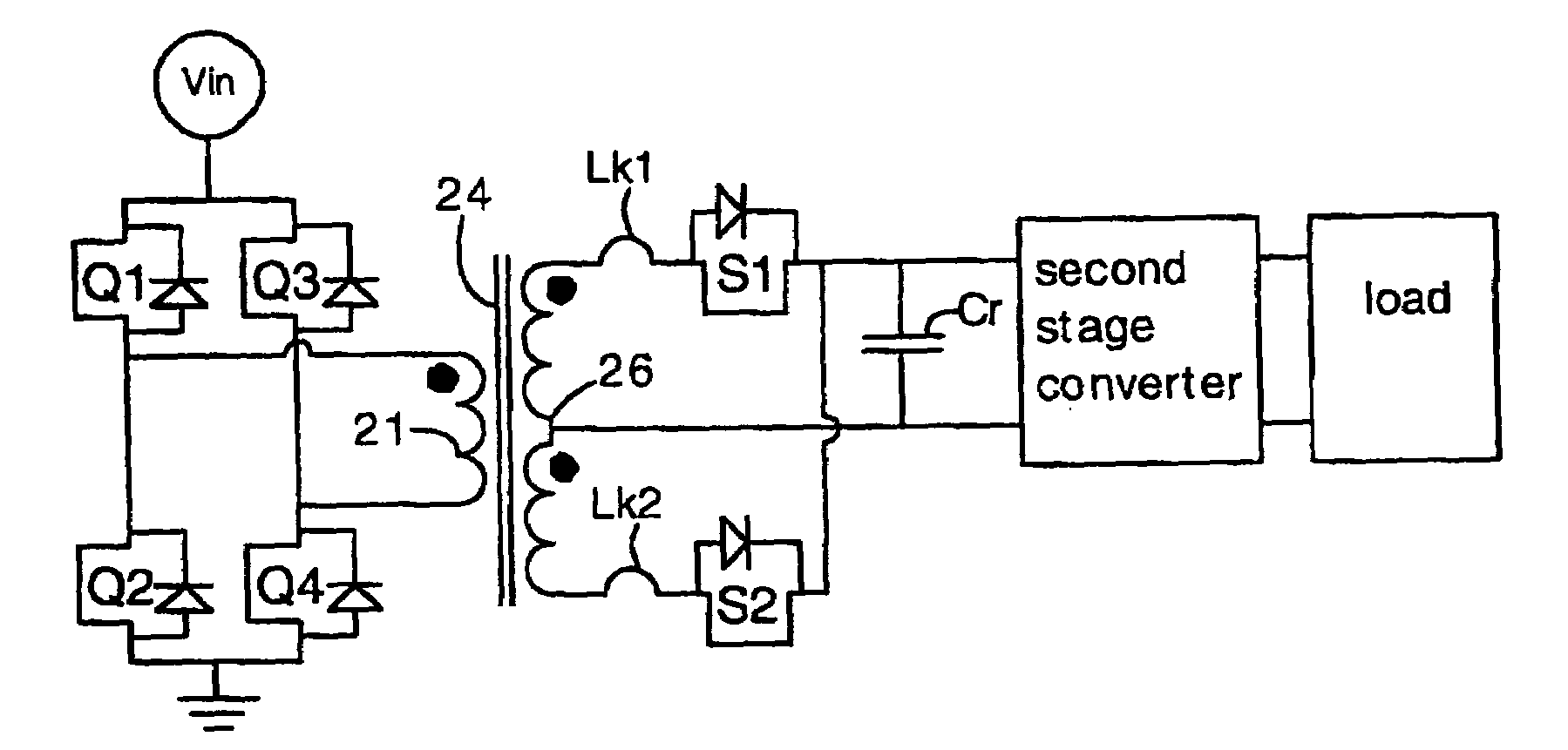
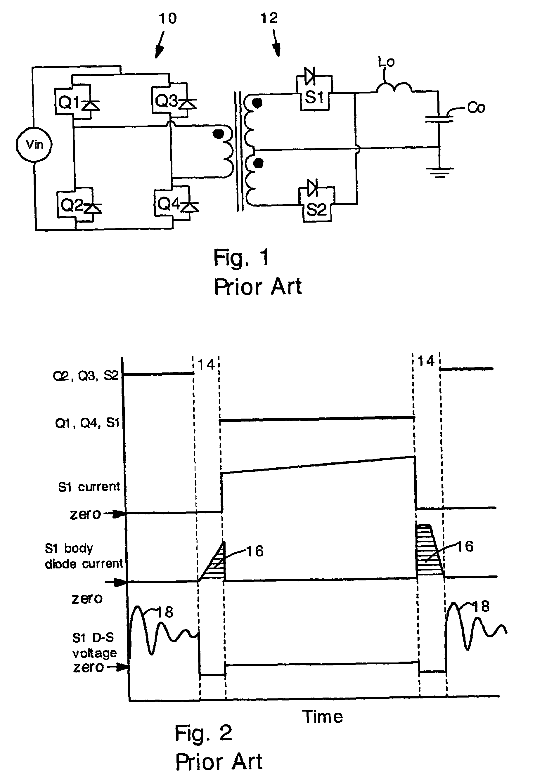
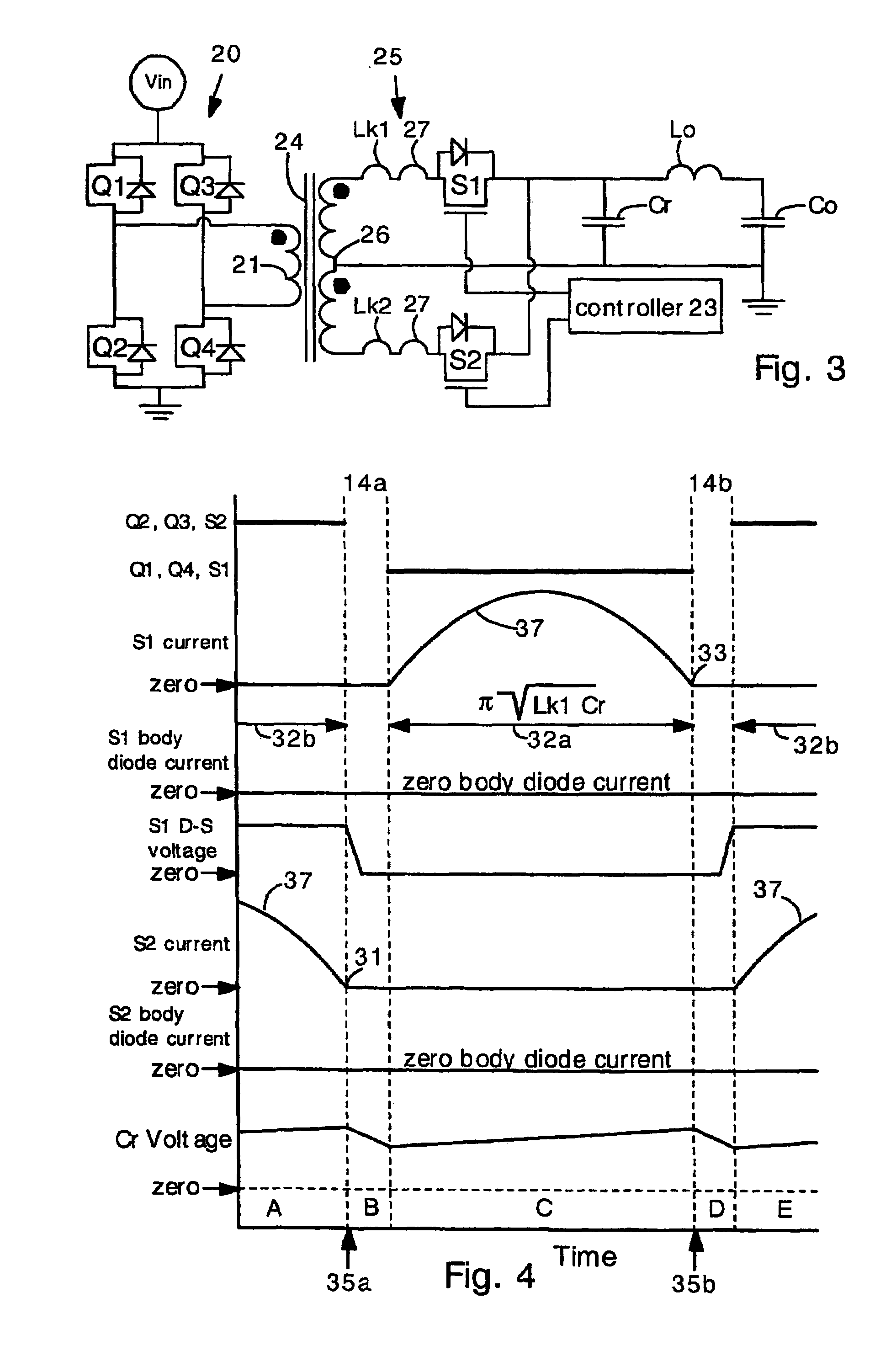
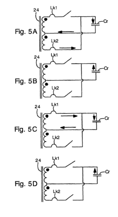
Power converters having capacitor resonant with transformer leakage inductance
PatentInactiveUS7196914B2
Innovation
- A power converter design featuring a resonant capacitor and leakage inductance that resonate to produce sinusoidal current pulses, reducing body diode conduction and reverse recovery losses, and enabling zero-voltage switching, with the resonant frequency aligned to the ON time of secondary switches to minimize voltage spikes and ringing.
Power converters having output capacitor resonant with autotransformer leakage inductance
PatentInactiveUS7254047B2
Innovation
- A power converter design incorporating a resonant capacitor and leakage inductance that resonates at half the LC period of the switch ON time, producing sinusoidal current pulses and enabling zero-voltage switching, reducing body diode conduction and reverse recovery losses, and allowing the use of low ON-state resistance switches.
Thermal Management Strategies
Thermal management represents a critical factor in optimizing tunnel diode efficiency within power converter applications. As tunnel diodes operate, they generate significant heat due to their high current density characteristics, particularly at the junction region. This thermal buildup directly impacts the negative differential resistance (NDR) region performance, which is essential for efficient power conversion operations. Effective thermal management strategies must address both steady-state and transient thermal conditions to maintain optimal operating temperatures.
Heat dissipation techniques specifically designed for tunnel diode implementations include advanced substrate materials with superior thermal conductivity properties. Silicon carbide (SiC) and aluminum nitride (AlN) substrates have demonstrated 30-40% improvement in heat transfer compared to traditional silicon-based substrates when implemented in tunnel diode power converter circuits. These materials facilitate more efficient heat spreading from the active junction areas to heat sinks or ambient environments.
Micro-channel cooling systems represent another promising approach for tunnel diode thermal management. These systems utilize miniaturized fluid channels positioned directly beneath or adjacent to the diode junction areas. Research indicates that properly designed micro-channel cooling can maintain junction temperatures within 5-10°C of ambient conditions even under high-power operation scenarios, significantly extending the NDR region stability and operational lifetime of tunnel diodes.
Phase-change materials (PCMs) offer complementary thermal buffering capabilities for handling transient thermal loads in tunnel diode applications. By absorbing heat during peak operation periods and releasing it during low-power phases, PCMs help maintain more consistent junction temperatures. Recent developments in metallic-organic PCMs have shown particular promise, with thermal capacities exceeding 200 J/g and phase transition temperatures precisely engineered to match tunnel diode optimal operating ranges.
Computational fluid dynamics (CFD) modeling has become essential for optimizing thermal management systems in advanced tunnel diode implementations. Three-dimensional thermal simulations enable precise prediction of hotspot formation and thermal gradients across the device structure. These models have revealed that asymmetric cooling approaches, which concentrate cooling resources at the junction periphery rather than directly beneath it, can improve thermal performance by up to 25% compared to conventional symmetric cooling designs.
Integration of on-chip temperature sensors and adaptive thermal management systems represents the cutting edge of tunnel diode thermal control. These systems continuously monitor junction temperatures and dynamically adjust operating parameters or cooling resources to maintain optimal thermal conditions. Experimental implementations have demonstrated efficiency improvements of 15-20% in power conversion applications by preventing thermal runaway conditions and maintaining operation within the optimal NDR region temperature range.
Material Science Innovations
Material science innovations have become a cornerstone for enhancing tunnel diode efficiency in power converter applications. Recent advancements in semiconductor materials have led to significant improvements in the negative differential resistance (NDR) characteristics of tunnel diodes, directly impacting their performance in high-frequency power conversion systems. The introduction of novel III-V compound semiconductors, particularly those incorporating gallium arsenide (GaAs) and indium phosphide (InP) heterostructures, has demonstrated superior electron tunneling properties compared to traditional silicon-based diodes.
The manipulation of material bandgap through precise doping techniques has emerged as a critical factor in optimizing tunnel diode efficiency. Research indicates that heavily doped p-n junctions with abrupt interfaces can significantly reduce the tunneling barrier width, thereby enhancing the peak-to-valley current ratio (PVCR) - a key performance indicator for tunnel diodes in power conversion applications. Experimental results show that achieving doping concentrations exceeding 10^19 cm^-3 on both sides of the junction can increase PVCR values by up to 40% compared to conventional designs.
Nanoscale material engineering has opened new avenues for tunnel diode enhancement. The integration of quantum well structures and atomically precise epitaxial growth techniques has enabled the development of resonant tunneling diodes (RTDs) with exceptional switching speeds and reduced power losses. These structures, when properly designed with optimal quantum well widths between 2-5 nm, demonstrate significantly improved negative resistance regions that are crucial for efficient power conversion.
The emergence of two-dimensional materials represents another breakthrough in tunnel diode technology. Graphene-based tunnel junctions have shown promising results due to their unique electronic properties, including high carrier mobility and tunable work functions. When combined with transition metal dichalcogenides (TMDs) in vertical heterostructures, these materials create atomically thin tunnel barriers with precisely controlled electronic properties, potentially revolutionizing the efficiency metrics of power converters operating at terahertz frequencies.
Temperature stability of tunnel diode materials has been substantially improved through the incorporation of wide-bandgap semiconductors such as gallium nitride (GaN) and silicon carbide (SiC). These materials maintain their tunneling characteristics across broader temperature ranges, addressing a critical limitation in conventional tunnel diodes. Recent studies demonstrate that GaN-based tunnel diodes can maintain over 85% of their room temperature efficiency at elevated temperatures up to 200°C, making them particularly valuable for high-power density converter applications in harsh environments.
Unlock deeper insights with Patsnap Eureka Quick Research — get a full tech report to explore trends and direct your research. Try now!
Generate Your Research Report Instantly with AI Agent
Supercharge your innovation with Patsnap Eureka AI Agent Platform!