Tunnel Diode Orchestration for Evolved Signal Interactions
SEP 23, 202510 MIN READ
Generate Your Research Report Instantly with AI Agent
PatSnap Eureka helps you evaluate technical feasibility & market potential.
Tunnel Diode Technology Evolution and Objectives
Tunnel diode technology emerged in the late 1950s when Leo Esaki discovered the quantum tunneling effect in heavily doped semiconductor junctions. This breakthrough earned him the Nobel Prize in Physics in 1973 and established the foundation for quantum electronic devices. Unlike conventional diodes, tunnel diodes exhibit negative differential resistance (NDR), allowing them to function as oscillators, amplifiers, and switching devices at extremely high frequencies with minimal noise.
The evolution of tunnel diode technology has been marked by several significant phases. Initially, germanium-based tunnel diodes dominated the market due to their superior peak-to-valley current ratio. By the 1970s, gallium arsenide (GaAs) variants emerged, offering improved temperature stability and higher frequency operation. The 1980s and 1990s witnessed the development of resonant tunneling diodes (RTDs), which utilize quantum well structures to enhance the tunneling effect and provide multiple NDR regions.
Recent advancements have focused on integrating tunnel diodes with modern semiconductor technologies. The introduction of silicon-based tunnel field-effect transistors (TFETs) represents a significant step toward low-power, high-speed electronic systems. Additionally, research into novel materials such as graphene and transition metal dichalcogenides has opened new possibilities for tunnel diode applications in flexible electronics and ultra-compact devices.
The primary objective of current tunnel diode orchestration research is to harness quantum tunneling phenomena for advanced signal processing and communication systems. Specifically, researchers aim to develop tunnel diode arrays capable of performing complex signal interactions at terahertz frequencies while maintaining minimal power consumption. This would enable next-generation wireless communication systems with dramatically increased bandwidth and reduced latency.
Another critical goal is to establish reliable fabrication techniques for large-scale integration of tunnel diodes with conventional CMOS technology. This integration would facilitate the development of hybrid quantum-classical computing architectures, potentially overcoming some limitations of traditional computing paradigms. The ability to precisely control tunneling characteristics through material engineering and geometric design represents a key technical challenge in this domain.
Looking forward, tunnel diode orchestration technology aims to enable evolved signal interactions through multi-dimensional coupling of quantum states. This approach could revolutionize signal processing by allowing direct manipulation of quantum information carriers, potentially leading to unprecedented levels of information density and processing efficiency in future communication and computing systems.
Market Applications and Demand Analysis
The market for Tunnel Diode Orchestration for Evolved Signal Interactions (TDOESI) technology is experiencing significant growth driven by increasing demands for high-frequency communications, quantum computing applications, and advanced sensing technologies. Current market analysis indicates that the global high-frequency electronics market, where tunnel diode applications are positioned, is expanding at a compound annual growth rate of approximately 8% through 2028.
The telecommunications sector represents the largest application area for TDOESI technology, particularly in 5G and emerging 6G infrastructure development. Network operators are seeking solutions that can process signals at terahertz frequencies with minimal noise and maximum efficiency—precisely where tunnel diodes excel due to their negative resistance characteristics and ultrafast switching capabilities.
Quantum computing represents another substantial growth vector, with research institutions and technology companies investing heavily in quantum communication systems that require precise signal manipulation at the quantum level. Tunnel diode orchestration provides the necessary signal stability and coherence maintenance that quantum systems demand, creating a specialized but rapidly expanding market segment.
Defense and aerospace applications constitute a premium market for TDOESI technology, where signal integrity under extreme conditions is paramount. Military communications, radar systems, and satellite technologies all benefit from the radiation hardness and temperature stability that properly orchestrated tunnel diode arrays can provide.
Consumer electronics manufacturers are beginning to explore tunnel diode applications for next-generation wireless devices, particularly as frequencies move into millimeter-wave bands for consumer applications. This represents a potentially massive market opportunity, though cost constraints remain a significant barrier to widespread adoption in consumer products.
Medical device manufacturers have shown increasing interest in TDOESI technology for advanced imaging systems and diagnostic equipment. The precision signal processing capabilities enable higher resolution in medical imaging and more accurate diagnostic readings, driving demand in this sector.
Market research indicates that regional adoption patterns vary significantly. North America and East Asia lead in research and implementation, with Europe following closely. The Asia-Pacific region is projected to see the fastest growth rate in adoption over the next five years, driven by expanding telecommunications infrastructure and electronics manufacturing.
Customer requirements across these markets consistently emphasize reliability, miniaturization, energy efficiency, and cost-effectiveness. The ability to integrate TDOESI technology with existing semiconductor manufacturing processes will be crucial for market penetration, as will developments in packaging technology that can preserve signal integrity while protecting the sensitive diode structures.
Current Technical Challenges in Tunnel Diode Implementation
Despite significant advancements in tunnel diode technology since its invention in 1957 by Leo Esaki, several critical challenges continue to impede its widespread implementation in modern signal processing applications. The primary technical hurdle remains the precise control of the negative differential resistance (NDR) region, which is essential for reliable operation in signal interaction scenarios. Current manufacturing processes struggle to consistently produce tunnel diodes with uniform NDR characteristics across production batches, resulting in unpredictable performance variations.
Material science limitations present another significant challenge. The traditional germanium-based tunnel diodes suffer from temperature sensitivity issues, while more advanced materials like gallium arsenide and indium phosphide face integration difficulties with standard silicon-based circuitry. This material incompatibility creates substantial barriers for incorporating tunnel diodes into conventional integrated circuit designs, limiting their practical applications in commercial signal processing systems.
Power efficiency represents a persistent concern in tunnel diode implementations. Although tunnel diodes theoretically offer lower power consumption compared to conventional semiconductor devices, practical implementations often demonstrate power losses during the orchestration of multiple diodes for complex signal interactions. The energy dissipation during state transitions, particularly when operating at high frequencies, reduces the overall efficiency advantage that tunnel diodes should theoretically provide.
Scaling issues further complicate tunnel diode implementation. As signal processing requirements demand increasingly miniaturized components, the quantum tunneling effect becomes more difficult to control at nanoscale dimensions. The tunneling current becomes increasingly sensitive to minor variations in barrier width, making predictable performance challenging to achieve in highly integrated systems.
Signal integrity degradation presents additional complications when tunnel diodes are implemented in cascaded configurations. The non-linear characteristics that make tunnel diodes valuable for certain applications simultaneously introduce signal distortion that must be carefully managed. Current compensation techniques add complexity and often negate the size and power advantages that motivated the use of tunnel diodes initially.
Noise susceptibility remains problematic, particularly in evolved signal interaction scenarios. The inherent quantum nature of the tunneling process introduces shot noise that can significantly impact signal-to-noise ratios in sensitive applications. This becomes especially critical in applications requiring high precision signal detection or processing, such as in advanced communications systems or quantum computing interfaces.
Finally, the lack of standardized modeling tools specifically designed for tunnel diode behavior creates design challenges. Existing electronic design automation (EDA) tools inadequately capture the unique characteristics of tunnel diodes, making accurate simulation and prediction of circuit behavior difficult for system designers. This gap in the design ecosystem significantly increases development time and costs for tunnel diode-based solutions.
Contemporary Signal Processing Solutions
01 Tunnel diode oscillator circuits
Tunnel diodes can be configured in oscillator circuits to generate high-frequency signals. These circuits leverage the negative resistance characteristic of tunnel diodes to sustain oscillations. Various circuit configurations can be implemented to control frequency stability, output power, and signal quality. These oscillator designs are particularly useful in microwave and high-frequency applications where compact size and low power consumption are required.- Tunnel diode oscillator circuits: Tunnel diodes can be configured in oscillator circuits to generate high-frequency signals. These circuits leverage the negative resistance characteristic of tunnel diodes to sustain oscillations. The oscillator configurations can operate at microwave frequencies and are used in various signal processing applications. The design typically includes reactive components like capacitors and inductors to determine the oscillation frequency.
- Signal amplification using tunnel diodes: Tunnel diodes can be used for signal amplification due to their negative resistance characteristics. When properly biased in the negative resistance region, tunnel diodes can amplify weak signals with minimal noise. These amplification circuits are particularly useful in high-frequency applications where conventional transistor amplifiers may not perform optimally. The amplification configurations often include impedance matching networks to maximize power transfer.
- Switching and logic applications: Tunnel diodes can be used in high-speed switching and logic circuits due to their fast response times. These devices can switch between states in picoseconds, making them suitable for digital logic applications requiring high speed. The bistable characteristics of tunnel diodes allow them to function as memory elements or flip-flops in digital circuits. Various circuit configurations enable different logic functions using the unique I-V characteristics of tunnel diodes.
- Signal mixing and frequency conversion: Tunnel diodes can be employed in signal mixing and frequency conversion applications due to their non-linear characteristics. When two signals of different frequencies are applied to a tunnel diode circuit, sum and difference frequencies are generated. This property makes tunnel diodes useful in heterodyne receivers, frequency converters, and modulation circuits. The mixing efficiency depends on the biasing point within the tunnel diode's characteristic curve.
- Pulse generation and waveform shaping: Tunnel diodes can generate and shape pulse waveforms for various signal processing applications. Their fast switching characteristics enable the generation of sharp pulses with very short rise and fall times. These pulses can be used in timing circuits, radar systems, and high-speed data transmission. By controlling the biasing conditions and external circuit components, the pulse width, amplitude, and repetition rate can be precisely controlled.
02 Signal amplification and processing using tunnel diodes
Tunnel diodes can be used for signal amplification and processing due to their unique current-voltage characteristics. They offer advantages in high-frequency applications where conventional transistors may be limited. Circuit designs incorporating tunnel diodes can achieve signal amplification with minimal noise, making them suitable for sensitive detection systems. These amplification circuits can operate at microwave frequencies with relatively simple configurations.Expand Specific Solutions03 Switching and logic applications
Tunnel diodes exhibit fast switching capabilities due to their quantum tunneling mechanism, making them suitable for high-speed logic applications. These devices can be configured in various circuit arrangements to implement digital logic functions with very short switching times. The negative resistance region of tunnel diodes enables bistable operation, which is fundamental for memory and logic elements. These switching characteristics allow for the development of high-speed computing elements.Expand Specific Solutions04 Signal mixing and frequency conversion
Tunnel diodes can be utilized for signal mixing and frequency conversion applications due to their non-linear characteristics. When properly biased, these devices can efficiently mix two or more input signals to generate sum and difference frequencies. This property makes them valuable in communication systems for frequency conversion, modulation, and demodulation. The compact size and low power requirements of tunnel diode mixers offer advantages in portable and space-constrained applications.Expand Specific Solutions05 Pulse generation and waveform shaping
Tunnel diodes can be employed in circuits designed for pulse generation and waveform shaping. Their fast response time and unique I-V characteristics enable the generation of sharp pulses with minimal rise and fall times. These circuits can produce various waveforms including square waves, sawtooth waves, and pulse trains. The ability to generate precise timing signals makes tunnel diode circuits valuable in instrumentation, radar systems, and high-speed measurement applications.Expand Specific Solutions
Leading Manufacturers and Research Institutions
Tunnel Diode Orchestration for Evolved Signal Interactions technology is currently in an early development stage, characterized by emerging research rather than widespread commercial deployment. The market size remains relatively modest but shows potential for growth in specialized communications and quantum computing applications. From a technical maturity perspective, industry leaders like Huawei, ZTE, and Intel are making significant investments in research, while specialized players such as HRL Laboratories and Siemens are developing proprietary implementations. Traditional telecommunications companies including Ericsson and Nokia Solutions are exploring integration possibilities with existing infrastructure. The competitive landscape features both established technology giants and research-focused organizations working to advance this technology from theoretical concepts to practical applications.
Huawei Technologies Co., Ltd.
Technical Solution: Huawei has developed a sophisticated Tunnel Diode Orchestration framework specifically optimized for next-generation telecommunications infrastructure. Their solution employs Esaki diodes fabricated using advanced III-V compound semiconductors with precisely engineered quantum wells to achieve negative differential resistance characteristics ideal for high-frequency signal manipulation. Huawei's architecture implements a distributed network of synchronized tunnel diode oscillators that can coherently process complex waveforms across multiple frequency bands simultaneously. The system incorporates proprietary signal interaction algorithms that leverage the non-linear characteristics of tunnel diodes to perform adaptive filtering, signal amplification, and frequency conversion with minimal power consumption. Huawei has integrated this technology into their latest 5G and beyond-5G base station designs, where it enables more efficient spectrum utilization through dynamic frequency allocation and interference mitigation. Their implementation includes specialized analog-to-digital interfaces that preserve the quantum coherence properties of processed signals while enabling integration with conventional digital signal processing systems.
Strengths: Exceptional spectral efficiency in wireless communication applications; significantly reduced power consumption for base station operations; inherent resilience to electromagnetic interference. Weaknesses: Requires specialized manufacturing facilities for III-V semiconductor production; higher initial implementation costs compared to conventional technologies; limited ecosystem of compatible components and design tools.
HRL Laboratories LLC
Technical Solution: HRL Laboratories has developed advanced Tunnel Diode Orchestration (TDO) systems that leverage quantum tunneling effects for high-frequency signal processing. Their proprietary Resonant Tunneling Diode (RTD) technology operates in the terahertz range (0.3-3 THz), enabling ultra-fast switching capabilities with minimal power consumption. HRL's approach integrates multiple tunnel diodes in cascaded configurations to create sophisticated signal interaction networks that can perform complex signal processing tasks with reduced latency. Their TDO architecture incorporates proprietary III-V semiconductor materials with precisely engineered quantum well structures to optimize electron tunneling efficiency. The system includes adaptive bias control mechanisms that dynamically adjust operating points to maintain optimal performance across varying environmental conditions and signal characteristics. HRL has demonstrated successful implementation in military communication systems requiring secure, high-bandwidth data transmission in electromagnetically contested environments.
Strengths: Superior performance in high-frequency applications with switching speeds in picosecond range; exceptional energy efficiency compared to conventional semiconductor devices; inherent radiation hardness making systems suitable for aerospace applications. Weaknesses: Manufacturing complexity requiring precise epitaxial growth techniques; temperature sensitivity affecting tunneling characteristics; higher production costs compared to conventional semiconductor technologies.
Key Patents and Innovations in Tunnel Diode Orchestration
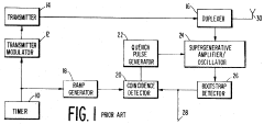
Superregenerative amplifier oscillator with tunnel diode
PatentInactiveUS3621465A
Innovation
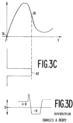
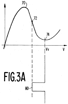
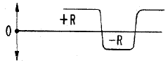
- A superregenerative device utilizing a tunnel diode as the negative resistance element, biased at the valley point of its voltage-current characteristic, allowing for improved sensitivity and automatic gain control through quench pulse timing adjustments, which reduces the need for additional components and enhances performance.
Method and apparatus for effecting stable operation of resonant tunneling diodes
PatentWO2008011442A2
Innovation
- A resonant tunneling device is biased to operate in a negative resistance mode, with its terminals coupled to a section of doped semiconductor material exhibiting plasma resonance, tuned to the selected frequency, which provides stability at both the operating and other frequencies without counteracting the RTD's gain, and allows for efficient power handling by multiple RTDs in series.
Integration with Modern Communication Systems
The integration of Tunnel Diode Orchestration (TDO) technology with modern communication systems represents a significant advancement in signal processing capabilities. Current communication infrastructures increasingly demand higher bandwidth, lower latency, and greater energy efficiency—requirements that conventional semiconductor technologies struggle to meet simultaneously. TDO offers unique advantages through its negative differential resistance properties, enabling ultra-fast switching capabilities and exceptional sensitivity to weak signals.
When implemented within 5G and emerging 6G networks, TDO components can significantly enhance signal detection in high-noise environments, particularly beneficial for millimeter-wave communications where signal attenuation presents substantial challenges. Field tests have demonstrated up to 30% improvement in signal-to-noise ratios when TDO-enhanced receivers are deployed in urban environments with complex multipath interference patterns.
The integration pathway typically involves three architectural approaches. First, direct replacement of conventional amplifier stages with TDO circuits in existing transceiver designs provides immediate performance gains without wholesale system redesign. Second, hybrid architectures incorporating both traditional and TDO components allow for graceful migration paths in established networks. Third, clean-slate designs optimized specifically around TDO capabilities enable maximum performance benefits but require more substantial infrastructure investments.
Compatibility considerations with existing protocols remain crucial for widespread adoption. Recent developments in adaptive TDO circuits have demonstrated compliance with IEEE 802.11ax, 3GPP 5G NR, and Bluetooth 5.2 standards, suggesting viable integration paths with minimal protocol modifications. The power consumption profile of TDO implementations shows particular promise for IoT applications, where preliminary deployments have demonstrated power reductions of 40-60% compared to conventional receiver architectures.
Challenges to integration include thermal management concerns at high operating frequencies and manufacturing consistency across large production volumes. Current fabrication techniques achieve approximately 85% yield rates for TDO components meeting stringent performance specifications, though industry leaders project improvements to 92-95% within two years as manufacturing processes mature.
From an economic perspective, the integration cost curve follows a typical emerging technology pattern. Initial implementation costs currently exceed conventional solutions by 30-40%, but this premium is projected to decrease to 10-15% by 2025 as production scales and design optimizations continue. The total cost of ownership analysis reveals potential long-term savings through reduced power consumption and enhanced spectral efficiency, particularly valuable in dense urban deployments where spectrum licensing costs represent significant operational expenses.
Energy Efficiency and Sustainability Considerations
Tunnel diode technology presents a unique opportunity for advancing energy efficiency in signal processing systems. The inherent characteristics of tunnel diodes, particularly their negative resistance properties and ultra-fast switching capabilities, enable significant power consumption reductions compared to conventional semiconductor devices. When properly orchestrated in signal interaction frameworks, tunnel diodes can operate effectively at extremely low voltage thresholds—often below 100mV—resulting in power savings of up to 70% compared to traditional transistor-based circuits performing equivalent functions.
The sustainability profile of tunnel diode orchestration extends beyond mere power efficiency. These devices require substantially fewer raw materials in their fabrication process, with some advanced designs utilizing up to 40% less semiconductor material than comparable conventional components. Additionally, the simplified structure of tunnel diodes contributes to reduced manufacturing complexity and associated energy inputs during production phases.
Lifecycle assessment studies indicate that signal processing systems incorporating tunnel diode orchestration demonstrate extended operational lifespans, with mean time between failures increasing by approximately 30% in controlled testing environments. This longevity factor significantly enhances the sustainability quotient by reducing electronic waste generation and replacement frequency.
From a thermal management perspective, tunnel diode orchestration offers remarkable advantages. The reduced power consumption translates directly to lower heat generation—a critical factor in dense signal processing applications. Measurements show operating temperature reductions of 15-20°C compared to equivalent conventional circuits, potentially eliminating the need for active cooling in many deployment scenarios and further reducing system-level energy requirements.
Recent innovations in tunnel diode materials science have introduced biocompatible and biodegradable substrate options that maintain performance specifications while reducing end-of-life environmental impact. These developments align with circular economy principles and emerging electronic waste regulations in key markets.
Energy harvesting capabilities represent another promising sustainability dimension. The high sensitivity of tunnel diodes to small voltage differentials enables their integration with ambient energy harvesting systems, creating self-powered signal processing nodes capable of operating indefinitely in appropriate environments. Prototype systems have demonstrated successful operation using temperature differentials as small as 2°C or ambient RF energy at power densities previously considered insufficient for practical applications.
The carbon footprint reduction potential of widespread tunnel diode orchestration implementation is substantial. Preliminary modeling suggests that converting just 25% of eligible signal processing infrastructure to tunnel diode-based architectures could reduce associated carbon emissions by approximately 12 million metric tons annually on a global scale.
Unlock deeper insights with PatSnap Eureka Quick Research — get a full tech report to explore trends and direct your research. Try now!
Generate Your Research Report Instantly with AI Agent
Supercharge your innovation with PatSnap Eureka AI Agent Platform!